Band structure model of magnetic coupling in semiconductors
Abstract
We present a unified band structure model to explain magnetic ordering in Mn-doped semiconductors. This model is based on the - and - level repulsions between the Mn ions and host elements and can successfully explain magnetic ordering observed in all Mn doped II-VI and III-V semiconductors such as CdTe, GaAs, ZnO, and GaN. This model, therefore, provides a simple guideline for future band structure engineering of magnetic semiconductors.
pacs:
75.50.Pp, 71.55.-i, 71.70.-dMn-doped II-VI and III-V diluted magnetic semiconductors (DMS) have many unique magneto-optical, magneto-electrical, and magneto-transport properties that are essential for future-generation spintronic device applications fur ; ohn ; die (a); aws ; wol . These materials also present many interesting behaviors. For example, Mn-doped II-VI semiconductors generally have antiferromagnetic (AFM) ground state, whereas Mn doped III-V semiconductors mostly have ferromagnetic (FM) ground state. Of great interest, some of the systems, such as Mn-doped GaN, can be either FM or AFM, depending on the Mn concentration, carrier density, or pressure dal . It will be, therefore, rewarding to understand the mechanism of magnetic coupling in these systems in order to design functional spintronic materials.
The mechanism that is responsible for the magnetic coupling in Mn doped III-V semiconductors has been widely discussed over the last few years die (b); lit ; sat ; schilf01 . Several models have been proposed to explain the phenomena, including the Zener/RKKY and, super- and double-exchange models. Although these models are quite successful in explaining some of the systems, they often lack universality and transparency, and are difficult to compare directly with ab initio band structure calculations. In this paper, using a band structure approach and level repulsion model, we will describe a unified picture to explain magnetic ordering in Mn-doped III-V and II-VI semiconductors and relate them to the previous models. We show that our model can successfully explain magnetic ordering observed in all Mn-doped II-VI and III-V semiconductors such as CdTe, GaAs, ZnO, and GaN. Therefore, it provides simple guidelines for future band structure engineering of magnetic semiconductors.
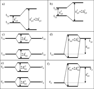
Our model is derived from the coupling and level repulsion between the magnetic ions and the host element’s states. When Mn atoms are incorporated into a semiconductor, they will introduce levels either inside the valence band or above the valence band maximum (VBM) of the semiconductor, depending on the host material. For example, for Mn in GaAs and CdTe, the occupied majority bands are below the host VBM, which contains mostly anion states. The unoccupied minority band is above the VBM. On the other hand, in ZnO and GaN, the levels are above the VBM. The introduced orbitals will interact with the host states forming hybrid orbitals. The hybrid orbitals will then also interact with each other. The hybridization occurs because the Mn states in a thetrahedral crystal field split into and states, whereas the VBM also has the symmetry, with large anion -character. The two states with the same symmetry can couple strongly with each other. Furthermore, without spin-orbit (SO) coupling, only the states with the same spin configuration can couple to each other so ; mon . Figure 1 shows the possible scenarios for the states that may couple to each other. In Fig. 1a, the host state is above the magnetic ion state, and the coupling leads to a level repulsion that pushes up the state by and pushes down the state by . In Fig. 1b, the state is above the state, and they are pushed up and down respectively by . Figure 1c shows the couplings between the two majority spin levels and the two minority spin levels, which lead to splittings and , respectively. Figure 1d shows the coupling between the majority spin state and the minority spin state, which pushes up the minority state by and pushes down the majority spin state by the same amount. The coupling between the states is similar to that of between the states, and they are described in Figs. 1e and 1f. In principle, the strenght of the interactions in Fig. 1 depends on the distance and orientation of the Mn pair. From these figures, we can see that there will be no energy gain if the two coupled states are fully occupied or fully empty. A magnetic state can be stabilized only if there are both holes and electrons in the coupled states.
In general, the - coupling is larger than the - coupling because the host orbital is more delocalized and Mn and anion are nearest neighbors. Within the - coupling, the coupling between the state is much weaker than the coupling between the state, because the state is very localized, whereas the state is less localized due to the coupling with the host states. Because the - coupling between the state is qualitatively similar to that of between the state, they are not discussed explicitly in our model. Furthermore, is smaller than when the exchange splitting is not zero because the level repulsion is larger if the energy separation of the two coupling states is small.
With the understanding above, in the following, we will discuss the mechanism of magnetic ordering observed in Mn doped II-VI and III-V semiconductors. In the discussion, we will use the two-band coupling model described in Fig. 1. First we will discuss the interaction between the and levels, and then the interaction between the levels. We will assume the coupling is additive. The small effect of coupled - and - interactions will be discussed briefly for simplicity, but in general, the treatment would not change the results qualitatively.
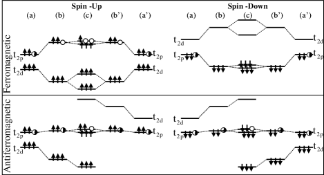
(i) We discuss first the scenario when the VBM is between the Mn majority and minority spin states. This is the case for most Mn-substituted II-VI and III-V systems such as CdMnTe and GaMnAs. A schematic plot is shown in Fig. 2, where the level repulsions are arranged in spin-up and spin-down channels in FM and AFM configurations. From (a) to (b) or (a’) to (b’), only the - coupling is turned on. From (b) and (b’) to (c), the - coupling is turned on. We first look at the FM configuration. In the spin-up channel, the - coupling pushes the state upward by , whereas it pushes down the state by the same amount far . The net energy gain in this process is , where is the number of holes. The - coupling further splits the levels by . Because all the majority spin levels are fully occupied, there is no energy gain in this process. (The - coupling is already included in the band structure calculation for the host, and its effect is the same for FM and AFM cases; therefore, it is not discussed here.) In the spin-down channel, the - coupling lowers the energy of the occupied spin-down state by . Because there are six electrons in the two states, the net energy gain in this case is . Therefore, the net energy gain for the FM configuration is . In the AFM configuration, the situation is the same in the spin-up and spin-down channel. When the - coupling is turned on, the state is pushed up by the occupied majority state by , but pushed down by the unoccupied minority state by . The occupied majority state is pushed down by , and it is further pushed down by the unoccupied minority state by . Therefore, the net energy gain in the AFM configuration is . Hence, taking into account the localization of the host orbitals around the Mn atoms far , the energy difference between the FM and AFM phase is
| (1) |
where decreases when the hole states become more localized, and when Mn-Mn distance increases. This result suggests that (a) the AFM phase is stabilized by the energy from coupling between the majority and minority spin states (often denoted as superexchange) dd . (b) The FM phase is stabilized with energy which is proportional to the number of holes and the - exchange splitting , as described in the Zener model. Therefore, to enhance FM coupling, one should increase the hole carrier density and increase the - exchange splitting. However, large - coupling also leads to large localization of the hole stae, thus, a balance between and is needed; (c) For systems where Mn substitution on the cation site does not introduce holes (e.g., CdMnTe), the system is always more stable in the AFM phase. (d) For systems where Mn substitution on the cation site introduces holes (e.g., GaMnAs, where each Mn on Ga site introduces one hole), because the - coupling is larger than the - coupling, the system in general will have a FM ground state if enough holes are present in the system. However, when holes are compensated by donor defects, the system can revert to the AFM ground state.
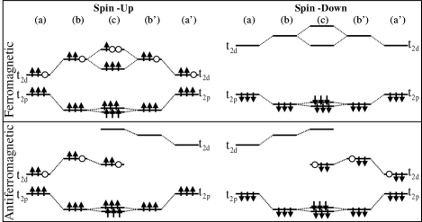
(ii) In the second scenario we discuss the case when the Mn state is above the VBM of the host. This is the the case for Mn in ZnO or in GaN. A schematic plot is shown in Fig. 3. The analysis is similar to that in the first scenario. In the FM configuration and spin-up channel, the system not only gains energy through the - coupling by , but also through the - coupling dd by , which put holes at a high energy level and electrons at a low energy level. Here, is the number of holes at the level, and for simplicity, we still use to describe the coupling between the VBM and the majority state. The energy gain in the spin-down channel is , thus the total energy gain for the FM configuration is . On the other hand, the net energy gain for the AFM configuration is , thus the energy difference between the FM and AFM phase is
| (2) |
These results indicate that when the system has holes at the -derived level instead of the orbital, (a) the stabilization of the FM or AFM phase is not directly related to the - exchange splitting, but is determined by the coupling dd terms (often denoted as double exchange) and terms. (b) When the number of holes decreases, the AFM phase is stabilized against the FM phase. When (e.g., ZnMnO), the system is always more stable in the AFM phase. (c) Whether the system has an FM or AFM ground state depends not only on hole carrier density, but also on the relative strength of FM stabilization energy , and the AFM stabilization energy . increases when the exchange splitting decreases. This can be achieved if the charge is transfered from the majority to minority spin state (e.g., from majority to minority state), thus reducing the magnetic moment and exchange splitting. The majority state can be pushed upward through increased - coupling, which can be realized by increasing Mn concentration or applying pressure. Thus, we predict that for Mn-doped GaN, when the Mn concentration is high or under pressure, the system will have an AFM ground state dal .
To test our models, we performed first-principles total-energy calculations for CdMnTe, GaMnAs, ZnMnO, and GaMnN. The calculations were performed using an ab initio plane wave basis code vas , based on the local spin density functional theory and using ultrasoft pseudopotentials usp . For the exchange and correlation potential, we used the generalized gradient approximation of Perdew and Wang pw (9). The Brillouin zone integration is performed using the Monkhost-Pack special k points scheme mon of 4x4x4 for the energy differences and 6x6x6 for the DOS, in a 64 atom supercell with two Mn atoms as first fcc neighbors. Interactions of further neighbors were considered elsewhere mon . We considered the zinc-blende alloy and assumed that the same results also hold for the alloy in a wurtzite structure.
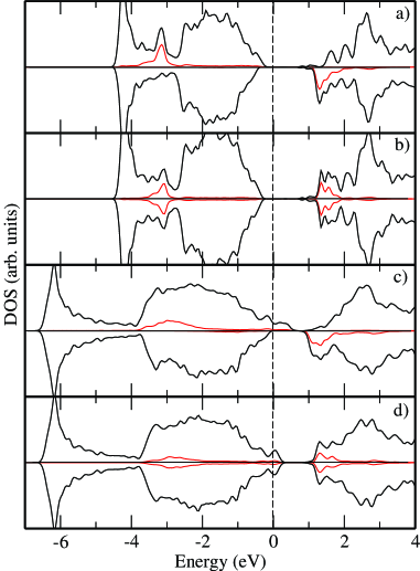
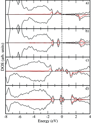
Figure 4 shows the total (black) and Mn projected (red) density of states for CdMnTe and GaMnAs in the FM and AFM configurations. We see that these two systems correspond to scenario (i) where the VBM is between the majority and minority Mn states. For CdMnTe, the substitution of Mn for Cd does not introduce holes (Figs. 4a and 4b), therefore, according to our model [Eq. (1)], the system should be AFM. For GaMnAs, holes are present in the VBM-derived states (Figs. 4c and 4d), therefore, our model predicts that it should be FM. Indeed, our directly calculated total energy differences between FM and AFM configurations for these two systems (Table I) agree with those expected from our model. Figure 5 shows the total (black) and Mn projected (red) density of states for ZnMnO and GaMnN in the FM and AFM configurations. We see that these two systems correspond to scenario (ii) where the VBM is below the Mn states. For ZnMnO, no holes are present when Zn is replaced by Mn (Figs. 5a and 5b), therefore, according to our model [Eq. (2)], the system should be AFM. For GaMnN with small Mn conccentration (6.25%), holes are created at the Mn -derived level, and the Mn has a high-spin configuration (Figs. 5c and 5d), thus our model predicts that it should have an FM ground state. Again, our direct calculations shown in Table I agree with what is expected from our model.
| (meV) | Ground state | |
|---|---|---|
| Cd1-xMnxTe | 35 | AF |
| Ga1-xMnxAs | -212 | F |
| Zn1-xMnxO | 110 | AF |
| Ga1-xMnxN | -225 | F |
In summary, we have proposed a model that can successfully explain the stabilization of the ferromagnetic or antiferromagnetic phases in Mn-doped II-VI and III-V semiconductors. This simple model is based on the - and - level repulsions between the Mn ions and host states and can be directly related to band parameters. Therefore, it should be very useful in understanding and engineering diluted magnetic semiconductors with desired properties. A similar model could also be developed to study other transition metals in semiconductors, as long as the position of the levels and the number of holes induced by it were known.
The work at NREL is funded by the U.S. Department of Energy, Office of Science, Basic Energy Sciences, under Contract No. DE-AC36-99GO10337 to NREL. XGG is supported by the Nature Science Fundation of China, Chinese Academy of Science, and National Science Foundation of China. AF and AJRS thank the support from CNPq and FAPESP.
References
- (1) Diluted magnetic Semiconductors, edited by J. K. Furdyna and J. Kossut, (Academic Press, Boston, 1988).
- (2) H. Ohno, Science 281, 951 (1998).
- die (a) T. Dietl, et al., Science 287, 1019 (2000).
- (4) D. D. Awschalom and R. K. Kawakami, Nature (London) 408, 923 (2000).
- (5) S. A. Wolf et al., Science 294, 1488 (2001).
- (6) G. M. Dalpian and S.-H. Wei, submitted.
- die (b) T. Dietl and H. Ohno, MRS Bulletin, October (2003), p. 714.
- (8) V. I. Litvinov and V. K. Dugaev, Phys. Rev. Lett. 86, 5593 (2001).
- (9) K. Sato, P. H. Dederics, and H. Katayama-Yoshida, Euro. Phys. Lett. 61, 403 (2003).
- (10) M. van Schilfgaarde, and O. N. Mryasov, Phys. Rev. B, 63, 233205 (2001).
- (11) In a first-order approximation, including spin-orbit coupling will not change the magnetic stability qualitatively. See Ref. 12.
- (12) A. J. R. da Silva, A. Fazzio, R. R. dos Santos, and L. E. Oliveira, J. Phys.: Cond. Matter 16, 8243 (2004).
- (13) Here we consider only first-order effects and assume that the states are delocalized so it couples with both Mn atoms. In higher-order perturbation theory, the state (and the hole) [K. S. Burch et al, Phys. Rev. B 70, 205208 (2004)] is more localized around the Mn atom, so when the Mn atoms move away from each other, the coupling between the Mn atom and the state localized around the other Mn atom is reduced. This will reduce the prefactor to be less than two and lead to an energy gain in the AFM case. The effect is equivalent to the reduced .
- (14) Although the coupling is denoted as - for simplification, due to the strong - hybridization between the and states, the states in (b), (b’), and (c) in Figs. 2 and 3 have mixed characters. Because of this hybridization, the so-called - coupling is not exactly a short-range interaction.
- (15) G. Kresse and J. Hafner, Phys. Rev. B 47, RC558 (1993); G. Kresse and J. Furthmuller, ibid. 54, 11169 (1996).
- (16) D. Vanderbilt, Phys. Rev. B 41, 7892 (1990).
- pw (9) J. P. Perdew and Y. Wang, Phys. Rev. B 45, 13244 (1992).
- (18) H. J. Monkhorst and J. P. Pack, Phys. Rev. B 13, 5188 (1976).