High-energy spectroscopic study of the III-V nitride-based
diluted magnetic semiconductor Ga1-xMnxN
Abstract
We have studied the electronic structure of the diluted magnetic semiconductor Ga1-xMnxN ( = 0.0, 0.02 and 0.042) grown on Sn-doped -type GaN using photoemission and soft x-ray absorption spectroscopy. Mn -edge x-ray absorption have indicated that the Mn ions are in the tetrahedral crystal field and that their valence is divalent. Upon Mn doping into GaN, new state were found to form within the band gap of GaN, and the Fermi level was shifted downward. Satellite structures in the Mn 2 core level and the Mn 3 partial density of states were analyzed using configuration-interaction calculation on a MnN4 cluster model. The deduced electronic structure parameters reveal that the - exchange coupling in Ga1-xMnxN is stronger than that in Ga1-xMnxAs.
pacs:
75.50.Pp, 75.30.Hx, 79.60.-i, 78.70.DmI Introduction
Diluted magnetic semiconductors (DMS) have recently attracted much interest because of novel functions and potential applications of the combination of magnetism caused by the local spins of transition-metal ions and semiconducting properties due to the itinerant carriers of the host materials. In the II-VI and III-V DMS such as Cd1-xMnxTe and Ga1-xMnxAs, the 3 transition-metal ions are substituted for the cations of the host semiconductors. In Ga1-xMnxAs, the ferromagnetism is induced by the hole carriers created by the substitution of the divalent Mn ions for the trivalent cations. This ferromagnetism is therefore called “carrier-induced ferromagnetism”. From the view point of applications, it is required to synthesize DMS with a Curie temperature () above the room temperature. So far, the of the III-V DMS has been mostly below the room temperature. In recent theoretical studies, it has been predicted that the ferromagnetic state is stable in Ga1-xMnxN Sato ; Mahadevan and that the ferromagnetism with a very high realized in wide-gap systems such as -type Ga1-xMnxN Dietl . After the successful Mn doping into GaN Kuwabara ; Zajac1 , several groups indeed reported that Ga1-xMnxN shows indication of ferromagnetism Sonoda ; Overberg ; Chen ; Hashimoto ; Yu . However, these results have been quite diverse between different reports and the occurrence of ferromagnetism remains controversial. Ando has reported that magnetic circular dichroism (MCD) of Ga1-xMnxN shows a paramagnetic behavior Ando . It is also possible that Mn-N or Ga-Mn compounds are formed in the crystal and contribute to the ferromagnetic properties Kuwabara ; Dhar ; Zajac2 . It is therefore desirable to characterize the electronic structure of Ga1-xMnxN to see whether there is an intrinsic possibility of high-temperature ferromagnetism in this system.
High-energy spectroscopic methods such as photoemission spectroscopy and soft x-ray absorption spectroscopy are powerful techniques to investigate the electronic structure of solids. In the studies of DMS, too, these techniques have played important roles Jun ; Wi . In this work, we have investigated the electronic structure of Ga1-xMnxN using photoemission spectroscopy, soft x-ray absorption spectroscopy (XAS) and subsequent configuration-interaction (CI) cluster-model analysis. The CI approach is a useful tool to describe such systems in which Coulomb interaction on the transition-metal atom and strong hybridization between the transition-metal and surrounding atoms coexist. The electronic structure parameters can be estimated by analyzing the core-level and valence-band photoemission spectra of DMS, enabling us to estimate the magnitude of the interaction between the localized 3 spins and itinerant carriers.
II experimental
The photoemission experiments were performed at BL-18A of Photon Factory, High Energy Accelerator Research Organization (KEK). Photoelectrons were collected using a VG CLAM hemispherical analyzer in the angle-integrated mode. The total energy resolution including the monochromator, the electron analyzer and the temperature broadening was 200 meV as estimated from the Fermi edge of a metal. Core-level x-ray photoemission (XPS) spectra were taken using a JEOL JPS-9200 hemispherical analyzer equipped with a Mg source (h = 1253.6 eV) with the resolution of 800 meV. Ghosts of the source due to the , and lines have been numerically subtracted. The photoemission spectra were referenced to the Fermi edge of a metal in electrical contact with the sample. All the measurements were made in an ultra-high vacuum below 510-10 Torr at room temperature. The x-ray absorption spectroscopy measurements were performed at the soft x-ray beam line BL-23SU of SPring-8. Absorption spectra were measured by the total electron yield method with the energy resolution / higher than 10000.
Ga1-xMnxN (0001) thin films with = 0.0, 0.02 and 0.042 were grown by molecular beam epitaxiy with an RF-plasma nitrogen source and elemental sources of Ga and Mn on a sapphire (0001) Kondo . After nitridation of the substrate, an AlN buffer layer (3 nm) was grown on the substrate at the substrate temperature = 750 ∘C followed by the growth of a GaN buffer layer (100 nm) at = 700 ∘C. On top of the GaN layer, Sn-doped -type GaN layer (110 nm) was grown to secure the conduction of the sample. Finally, a Ga1-xMnxN epitaxial layer (110 nm) was deposited on top of it at the substrate temperature of 550 ∘C. All the samples thus prepared were paramagnetic from room temperature down to 4 K. For surface cleaning, we made N ion sputtering, which compensates the loss of N atoms, followed by annealing up to 500∘C because Ar+ ion preferentially sputters N atoms and may induce excess Ga atoms to form Ga clusters on the surface Lai . We have confirmed that the photoemission spectra did not change by annealing. The cleanliness of the surface was checked by low-energy electron diffraction (LEED) and core-level XPS. The O 1 and C 1 core-level peaks were diminished below the detectability limit by repeating N ion-sputtering and annealing, and clear a LEED pattern was obtained, reflecting ordered clean surfaces.
III results and discussion
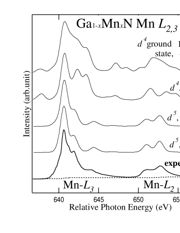
Figure 1 shows an XAS spectrum at the Mn -edge compared with atomic multiplet calculations for the and ground states. The rich structures of the observed spectrum show a multiplet splitting and are typical for localized 3 states. Comparing the experimental line shape with the calculation, one can obtain the information about the valence and the crystal field of Mn in Ga1-xMnxN. From Fig. 1, one can see that the calculation assuming the ground state with the tetrahedral-crystal field 10 -0.5 eV well represents the experimental spectrum. The negative 10 means a crystal field due to the tetrahedrally coordinating anions, while positive 10 means a crystal field with octahedral symmetry such as the interstitial position in the wurtzite structure Popovic . This leads us to conclude that most of Mn atoms in the sample used in the present measurements are in the state, namely, the valence of Mn is divalent with the total spin = 5/2 and in the tetrahedral crystal field. A similar line shape of the absorption spectra of Ga1-xMnxN and a similar conclusion about the valence state have been reported Edmonds . This is also consistent with the previous report about the valence state of Mn in GaN based on the Curie-Weiss behavior of the magnetic susceptibility data Kuwabara . On the other hand, the valence state of Mn in non-doped GaN has been reported to be trivalent based on electron spin resonance and optical absorption Graf1 . The reason for this difference is not clear at present, but it has also been reported that Mn is divalent when electrons are doped Graf2 whereas Mn is tetravalent when holes are doped Korotkov . It has also been reported that the charge transfer occurs across adjacent layer in Ga1-xMnxN/p-GaN:Mg and Ga1-xMnxN/n-GaN:Si heterostructures Arkun . In that report, it has been indicated that a large number of electrons (holes) are transferred from adjacent n-type (p-type) layer into the sample. The difference thus may be explained by the scenario of the charge transfer from Sn-doped -type GaN to Ga1-xMnxN (i.e., electron doping into Ga1-xMnxN).
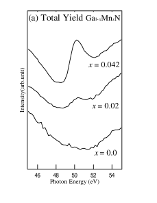
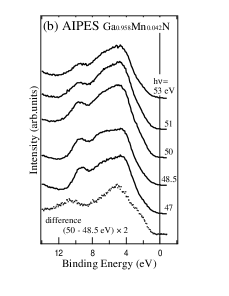
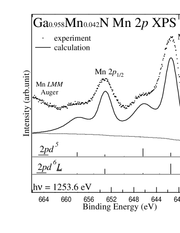
Figure 2 shows the Mn 2 core-level photoemission spectra of the = 0.042 sample. The broad peak at 667 eV is due to overlapping Mn Auger emission. The spectra show a spin-orbit doublet, each component of which shows a satellite structure on the higher binding energy side separated by 5 eV. The presence of the satellite structure indicates strong Coulomb interaction among the 3 electrons and strong hybridization between the 3 electrons and the host valence electrons.
In order to analyze the satellite structure and to obtain the electronic structure parameters, atomic multiplet theory has to be extended to the CI cluster model in order to take into account charge transfer effects. We have employed a tetrahedral MnN4 cluster with the central Mn atom. Here, the small distortion from the tetrahedron in the wurtzite structure is ignored. In the CI picture, the wave function of the ground state is given by a linear combination of , , , , where denotes a hole in the ligand orbitals. The final states of Mn 2 photoemission spectra are given by linear combinations of , , , , where stands for a Mn 2 core hole . The anion-to-3 orbital charge-transfer energy is = - , and the 3-3 Coulomb interaction energy is defined by = + - 2, where ) denoted the center of gravity of the multiplet. The average attractive Coulomb energy between the Mn 3 electron and the Mn 2 core hole has been fixed at / = 0.8. The transfer integrals between the 3 and ligand orbitals are given by Slater-Koster parameters () and () assuming the relationship ()/() = -2.16 Harrison . The calculated spectrum has been broadened with a Gaussian and a Lorentzian. We have assumed that the valence of the Mn is divalent according to the XAS result. We have also ignored additional holes which enter into the top of the valence band of GaN because the carrier concentration in the present samples is negligibly small, judged from the very high resistivity, presumably due to charge compensation. Thus, the satellite structures are well reproduced with parameter values = 4.0 1.0, = 6.0 1.0 and () = -1.5 0.1 eV.
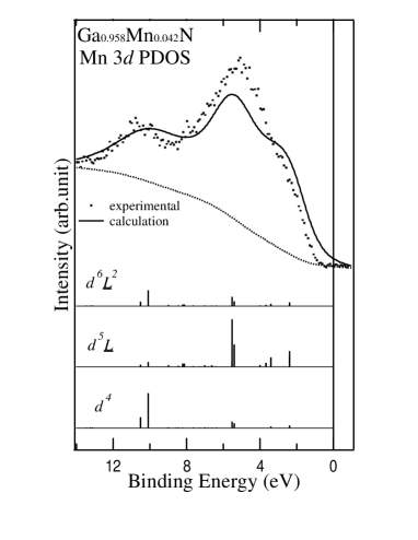
We have also investigated the valence band using resonant photoemission spectroscopy (RPES) to extract the Mn 3 partial density of states (PDOS). In RPES, because Mn 3-to-3 absorption occurs at photon energies above 50 eV, interference between the normal photoemission and 3-to-3 transition followed by a 3-3-3 super-Coster-Krönig decay generates a resonance enhancement of the Mn 3-drived photoemission. Figure 3 (a) shows the absorption spectra near the Mn 3-3 core excitation threshold of Ga1-xMnxN measured by the total electron yield method. In the Fig. 3 (a), one can see that with increasing , a peak appears at 50 eV and grows in intensity, representing the Mn 3-to-3 absorption. From these spectra, on-resonance and off-resonance photon energies are found to be 50 and 48.5 eV, respectively. Figure 3 (b) shows the valence-band spectra of the = 0.042 sample taken at various photon energies in the Mn 3-to-3 core excitation region. The intensities have been normalized to the photon flux. All binding energies are referenced to the Fermi level (). In going from h = 47 to 50 eV, one can see that the peak at the binding energy of 5 eV grows in intensity. By subtracting the off-resonant spectrum from the on-resonant one, we obtained the Mn 3 derived spectrum as shown in the bottom panel of Fig. 3 (b). For the subtraction, the photon energy dependence of the photoionization-cross section of the N 2 atomic orbital has been considered. The difference spectrum that corresponds to the Mn 3 PDOS reveals a peak at = 5 eV and a shoulder at = 2 eV. The shoulder is located at 0.5 eV above VBM and well below the Fermi level due to charge compensation. The satellite also appears at = 9 - 13 eV, at a higher binding energy than that of Ga1-xMnxAs Jun .
| Material | Reference | ||||
|---|---|---|---|---|---|
| Ga1-xMnxN | 4.0 | 6.0 | -1.5 | -1.6 | This work |
| Ga1-xMnxAs | 1.5 | 3.5 | -1.0 | -1.0 | 14 |
| In1-xMnxAs | 1.5 | 3.5 | -0.8 | -0.7 | 27 |
| Zn1-xMnxO | 6.5 | 5.2 | -1.6 | -2.7 | 28 |
| Zn1-xMnxS | 3.0 | 4.0 | -1.3 | -1.3 | 28 |
| Zn1-xMnxSe | 2.0 | 4.0 | -1.1 | -1.0 | 28 |
| Zn1-xMnxTe | 1.5 | 4.0 | -1.0 | -0.9 | 28 |
CI cluster-model calculation has also been used to analyze the Mn 3 PDOS as shown in Fig. 4. One can see that the calculation well explains not only the main structure but also the satellite which could not be explained by the band-structure calculation Sato , with identical parameters as in the case of Mn 2 core-level within the error bars, = 4.0 1.0, = 6.0 1.0 and () = -1.5 0.1 eV. As shown in the bottom panels of Fig. 4, the main peak largely consists of final states and the satellite of final states because of . In Table 1, the parameter values for Ga1-xMnxN are compared with those of other DMS. , , and () for Ga1-xMnxN are large comparing with other III-V and II-VI DMS, except for Zn1-xMnxO for which , and () are large. The charge-transfer energy of Ga1-xMnxN is large because of the high electronegativity of the anion. The one-electron transfer integral () is large because of the small distance between Mn and the anion. The large value of may be attributed to the low polarizability of N atom.
Using the , and () values thus obtained, one can estimate the - exchange constant for the Mn2+ ion in the semiconductor host in the second order of perturbation with respect the hybridization term:
where is defined as = - /2. The valence band width has been fixed at 3 eV because the upper 3 eV of the host valence band primarily contributes to hybridization term although the total width of the host valance band is 5-6 eV band . The charge-transfer energy and the 3-3 Coulomb interaction energy are defined with respect to the lowest term of each multiplet. Using Racah parameters and of the free Mn2+ ion values ( = 0.119 eV and = 0.412 eV) Racah , and are given by = + (70 - 35)/9 + 7 and = + (14 - 7)/9 +14 + 7. The local spin is 5/2 for Mn2+ (). The value of thus estimated is -1.6 0.3 eV and is larger than that of other III-V DMS (see Table 1). While the differences between and , which contribute to the denominator of the equation, is similar for Ga1-xMnxN, Ga1-xMnxAs and In1-xMnxAs, () is large in Ga1-xMnxN, giving rise to the large in Ga1-xMnxN.
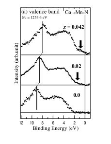
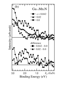
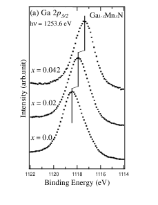
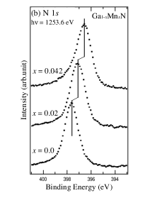
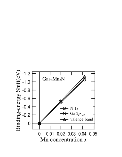
Finally, we show the Mn concentration dependence of the electronic structure of Ga1-xMnxN. The Ga 2 and N 1 core-level photoemission spectra in Fig. 5(a) and (b) clearly show shifts towards lower binding energies with increasing Mn concentration. Nearly the same amount of shifts were also observed in the valence-band spectra, as shown in Fig. 6(a). Note that these shifts cannot be due to charging effect because the electrical resistivity increases with Mn doping. Therefore, we conclude that the Fermi level is shifted downward with Mn doping, that is, the doped Mn atoms supply holes and compensate the electron carriers. From = 0 to 0.02 to 0.042, the amount of these shifts are 0.5 and 1.05 eV for N 1, 0.52 and 1.07 eV for Ga 2, 0.54 and 1.13 eV for the valence band. The shifts are linear with as shown in Fig. 7. In the valence-band spectra [Fig. 6 (a)], too, one can see that upon doping, new states are created above the VBM as shown by arrows. The new states are consistent with the result of a recent photoemission study using hard x-rays Kim . The spectra near the valence-band maximum are shown in Fig. 6 (b) and difference spectra from undoped GaN are shown in the bottom panel. Here, prior to the subtraction, the spectra of the = 0.02 and 0.042 have been shifted to higher binding energy so that the peak at 8eV is aligned. in order to deduce changes in the DOS induced by Mn doping. The new states are located at 0.5 eV above the VBM and are increased in intensity with increasing Mn concentration. This is considered as due to the appearance of Mn 3 character because in XPS the relative photoionization-cross section of Mn 3 to N 2 is as large as 10. If the holes doped through the Ga Mn substitution were not compensated, the acceptor level formed above the VBM would remain empty (i.e., above ) and would not be observed in the photoemission spectra. The new states above VBM are therefore considered to be the acceptor levels occupied by compensating electrons.
One of the reasons why ferromagnetism does not occur in Ga1-xMnxN samples used in this study in spite of the large - exchange constant may be the lack of a sufficient number of hole carriers which mediate ferromagnetic coupling between Mn ions. The new states above the VBM seen in Fig. 6(b) are consistent with this charge compensation picture. This suggests that if the compensation is reduced in some way and sufficient amount of holes are doped into the system, strong ferromagnetism would be expected.
IV conclusion
In conclusion, we have investigated the electronic structure of the diluted magnetic semiconductor Ga1-xMnxN using high-energy spectroscopy. It is confirmed that Mn in Ga1-xMnxN is divalent. We have treated the electronic structure as a many-electron system using CI analysis. The CI analysis of photoemission spectra on a MnN4 cluster model reveals that the magnitude of - exchange constant in Ga1-xMnxN is much larger than that in Ga1-xMnxAs. This implies the possibility that - exchange contributes to realize the room temperature ferromagnetism. Mn substitution indeed introduces holes into the system although most of them are compensated.
We thank T. Okuda, A. Harasawa and T. Kinoshita for their valuable technical support. This work was supported by a Grant-in-Aid for Scientific Research in Priority Area gSemiconductor Spintronics h (14076209) from the Ministry of Education, Culture, Sports, Science and Technology, Japan. One of us (HO) acknowledges support from German Academy Exchange Service. The experiment at Photon Factory was approved by the Photon Factory Program Advisory Committee (Proposal No. 2002G027).
References
- (1) K. Sato and H. Katayama-Yoshida, Jpn. J. Appl. Phys. 40, L485 (2001).
- (2) P. Mahadevan and A. Zunger, Appl. Phys. Lett. 85, 2860 (2004).
- (3) T. Dietl, H. Ohno, F. Matsukura, J. Cibert and D. Ferrand, Science 287, 1019 (2000).
- (4) S. Kuwabara, T. Kondo, T. Chikyow, P. Ahmet and H. Munekata, Jpn. J. Appl. Phys. 40, L724 (2001).
- (5) M. Zajac, R. Doradzinski, J. Gosk, J. SzcZytko, M. Lefeld-Sosnowska, M. Kaminska, M. Polczewska, E. Grzanska and W. Gebicki, Appl. Phys. Lett. 78, 1276 (2001).
- (6) S. Sonoda, S. Shimizu, T. Sasaki, Y. Yamamoto and H. Hori, J. Cryst. Growth. 237, 1358 (2002).
- (7) M. E. Overberg, C. R. Abernathy, S. J. Pearton, N. A. Theodoropoulou, K. T. McCarthy and A. F. Hebard, Appl. Phys. Lett. 79, 1312 (2001).
- (8) P. P. Chen, H. Makino, J. J. Kim and T. Yao, J. Cryst. Growth. 251, 331 (2003).
- (9) M. Hashimoto, Y. K. Zhou, H. Tampo, H. Kanamura and H. Asahi, J. Cryst. Growth. 252, 499 (2003).
- (10) Y. Y. Yu, R. Zhang, X. Q. Xiu, Z. L. Xie, H. Q. Yu, Y. Shi, B. Shen, S. L. Gu and T. D. Zheng, J. Cryst. Growth. 269, 7166 (2004).
- (11) K. Ando, Appl. Phys. Lett. 82, 100 (2003).
- (12) S. Dhar,O. Brandt, A. Trampert, L. Däweritz, K. J. Friedland, K. H. Ploog, J. Keller, B. Bescjpten and G. Güntherodt, Appl. Phys. Lett. 82, 2077 (2003).
- (13) M. Zajac, J. Gosk, E. Grzanska, M. Kaminska, A. Twardowski, B. Strojek, T. Szyszko and S. Podsiadlo, J. Appl. Phys. 82, 2077 (2003).
- (14) J. Okabayashi, A. Kimura, T. Mizokawa, A. Fujimori, T. Hayashi and M. Tanaka, Phys. Rev. B. 59, 2486 (1999).
- (15) S. C. Wi, J.-S. Kang, J. H. Kim, S.-B. Cho, B. J. Kim, S. Yoon, B. J. Suh, S. W. Han, K. H. Kim, K. J. Kim, B. S. Kim, H. J. Song, H. J. Shin, J. H. Shim and B. I. Min, Appl. Phys. Lett. 84, 4233 (2004). J. Appl. Phys. 95, 7166 (2004).
- (16) T. Kondo S. Kuwabara, H. Owa and H. Munekata, J. Cryst. Growth. 237, 1353 (2002).
- (17) Y. H. Lai, C. T. Yeh, J. M. Hwang, H. L. Hwang, C. T. Chen, W. H. Hung, J. Phys. Chem. B. 105, 10029 (2001).
- (18) Z. S. Popovic, S. Satpathy and W. C. Mitchel, Phys. Rev. B. 70, 161308 (2004).
- (19) K. W. Edmonds, N. R. S. Farley, T. K. Johal, R. P. Campion, B. L. Gallagher, C. T. Foxon and G. van der Laan, J. Appl. Phys. 95, 7166 (2003).
- (20) T. Graf, M. Gjukic, M. S. Brandt, M. Stutzmann and O. Ambacher, Appl. Phys. Lett. 81, 5159 (2002).
- (21) T. Graf, M. Gjukic, M. Hermann, M. S. Brandt, M. Stutzmann and O. Ambacher, Phys. Rev. B. 67, 165215 (2003).
- (22) R. Y. Korotokov, J. M. Gregie, B. Han and B. W. Wessels, Physica B 308, 18 (2001).
- (23) F. E. Arkun, M. J. Reed, E. A. Berkman, N. A. El-Masry, J. M. Zavada, M. L. Reed and S. M. Bedair, Appl. Phys. Lett. 85, 3809 (2004).
- (24) W. A. Harrison Electronic structure and the Properties of Solids (Dover, New York 1989).
- (25) A. Rubio, J. L. Corkill, M. L. Cohen, E. L. Shirley and S. G. Louie, Phys. Rev. B. 48, 11810 (1993).
- (26) S. Sugano, Y. Tanabe and H. Kamimura, Multiplets of Transition Metal Ions in Crystals (Academic, New York, 1970.)
- (27) J. Okabayashi, T. Mizokawa, D. D. Sarma and A. Fujimori, Phys. Rev. B. 65, 161203 (2002).
- (28) T. Mizokawa, T. Nambu, A. Fujimori, T. Fukumura and M. Kawasaki, Phys. Rev. B. 65, 085209 (2002)
- (29) J. J. Kim, H. Makino, P. P. Chen, T. Hanada, T. Yao, K. Kobayashi, M. Yabashi, Y. Takata, T. Tokushima, D. Miwa, K. Tamasaku, T. Ishikawa, S. Shin and T. Yamamoto, Material Science in Semiconductor Processing 6, 503 (2003).