Structural, electrical, and magneto-optical characterization of paramagnetic GaMnAs quantum wells
Abstract
Growth of GaMnAs by molecular beam epitaxy is typically performed at low substrate temperatures (C) and high As overpressures leading to the incorporation of excess As and Mn interstitials, which quench optical signals such as photoluminescence (PL). We report on optical-quality Ga1-xMnxAs/Al0.4Ga0.6As quantum wells (QWs) with % grown at a substrate temperature of C. Electrical and structural measurements demonstrate that this elevated temperature reduces As defects while allowing the substitutional incorporation of Mn into Ga sites. From a combination of Hall and secondary ion mass spectroscopy measurements we estimate that at least 70-90% of the Mn incorporates substitutionally in all samples studied. The incorporation behavior shows both a substrate temperature and QW width dependence. The low defect density of these heterostructures, compared to typical lower temperature grown GaMnAs, enables the observation of both polarization-resolved PL and coherent electron spin dynamics, from which the conduction band exchange parameter is extracted. No evidence of long-range Mn spin coupling is observed, whereas negative effective Curie temperatures indicate spin heating due to photoexcitation. Light Mn-doping maximizes the electron spin lifetime indicating the importance of the Dyakonov-Perel decoherence mechanism in these structures. PL spectra reveal a low energy peak from shallow donors, which because of the paramagnetic behavior of its PL polarization, we ascribe to Mn interstitials.
pacs:
71.70.Gm, 75.50.Pp, 78.47.+p, 61.72.VvI Introduction
Since the invention of the ferromagnetic semiconductor Ga1-xMnxAs, by Ohno et al.,Ohno:1996 it has been the subject of intense experimental work. The combination of electronic and magnetic properties in this system has enabled many interesting experimental demonstrations arising from the carrier-mediated nature of its ferromagnetism,Dietl:2001 which provides an excellent test bed for semiconductor spintronics since the host material system is a highly engineered optoelectronic semiconductor.Ohno:2004 ; Macdonald:2005 As a consequence of both the low solubility of Mn in GaAs and the high concentrations of substitutional Mn (MnGa) required for ferromagnetism to occur (5%, 1021cm, molecular beam epitaxy (MBE) growth at present is performed at low substrate temperatures (C ) and high arsenic overpressures. This is a regime of growth in which defects, chiefly excess As and Mn interstitials (Mni), are incorporated into the epilayers at concentrations that quench sensitive optical properties, such as photoluminescence (PL) and absorption. These optical properties can provide direct measurements of the energy splitting for spin-up and spin-down carriers at the band edges. In II-VI dilute magnetic semiconductors (DMS), for example, polarization-resolved magneto-PL or absorption have been used to extract the exchange constants.Dietl:1994 The ability to perform such optical measurements in GaMnAs is an important step in understanding the exchange interactions in this material.
Polarization-resolved PL spectroscopy is a useful tool for the measurement of conduction and valence band spin splittings in magnetic fields. PL techniques including measurements of the exciton Zeeman splitting, the Hanle effect, and the PL decay time have been used to determine electron and hole g-factors in semiconductor heterostructures.Snelling:1991 ; Snelling:1992 ; Traynor:1995 Additionally, the measurement of Kerr rotation (KR) or Faraday rotation (FR) serves as an extremely sensitive probe of magnetization, resolving less than 10 electron spins in bulk GaAs.Kato3:2004 This technique has led to a variety of advances in non-magnetic GaAs-based heterostructures including the electrical tuning of the g-factor,Salis:2001 ; Kato:2003 ; Poggio:2004 observation of strain induced spin-orbit interaction,Kato1:2004 ; Kato2:2004 and the measurement of the spin-Hall effect.Kato3:2004 In addition to electron spin dynamics, the technique has been used to measure magnetic ion spin coherence in II-VI ZnCdSe/MnSe quantum structures,Crooker:1996 and recently, in experiments demonstrating electrical control of the exchange enhanced electron spin splitting.Myers1:2004 The growth of optical-quality GaMnAs allows for the application of the aforementioned techniques and opens the door to a variety of measurements including the precise determination of the () exchange parameter, (), between electron spins in the s-like conduction (p-like valence) band and the 3d spins localized on Mn2+. From a practical standpoint, long electron spin lifetimes and compatibility with previously developed heterostructures for electron spin control favor the development of magnetically doped devices in GaAs-based III-V materials.
The purpose of this work is to develop the capability to grow GaMnAs structures by MBE in which coherent spin dynamics can be observed optically. Preliminarily, our growth campaign focused on achieving stoichiometric GaMnAs grown at a typical low temperature of C, at which the use of As overpressures leads to large concentrations of excess As. Stoichiometric growth can be achieved at low substrate temperatures by digital growth techniques, such as atomic layer epitaxy (ALE) in which the As flux is shutter controlled,Johnston:2003 or analog growth in which the As flux is controlled by source temperature and/or valve position. The former technique has enabled digital ferromagnetic heterostructures made up of sub-monolayers of MnAs with independent control of charge carriers in the non-magnetic GaAs spacer layers, while hybrid growths using both high temperature MBE (optical layer) and low temperature ALE (magnetic layer) have been developed to enable optical quality in GaAs-AlGaAs quantum wells (QWs) with a ferromagnetic barrier.Myers2:2004 Although polarization-resolved PL from these QWs demonstrates a spin coupling between the magnetic layer and carriers in the QWs, no time-resolved KR could be measured. In previous work using the As-valve for flux control, it was found that stoichiometric GaAs grown at C could be achieved as indicated by the low charge compensation of doped carriers (11016 cm; however, the incorporation of Mn at levels required for ferromagnetism could only be achieved by using an As overpressure. The resulting defects quenched both PL and time-resolved KR signals.Unpublished:1 In the current work we investigate MBE grown GaMnAs/AlGaAs QWs with low Mn-doping levels (%). At these Mn concentrations the substrate temperature can be increased to C while allowing substitutional incorporation of Mn. In contrast to low temperature stoichiometric growth, at the increased growth temperatures used here an As overpressure does not result in excess As incorporation, enabling the observation of PL and time-resolved electron spin dynamics in GaMnAs QWs.
Here we discuss structural, electrical, and magneto-optical properties with respect to the growth conditions and incorporation behavior of Mn in GaMnAs QWs. The effect of the substrate growth temperature (Tsub) on the incorporation of Mn is studied by secondary ion mass spectroscopy (SIMS) measurements of the Mn concentration profiles (Sec. III). The activation energy for Mn acceptors in the QWs is found by measuring the hole concentrations as a function of temperature using the Hall effect (Sec. IV). Comparison between the SIMS and Hall data allow us to estimate the fraction of MnGa acceptors incorporated in the QWs assuming that hole compensation is dominated by Mni donors (Sec. V). Time-resolved KR measurements indicate that Mn doping cm-3 maximizes the electron spin lifetime. These data show evidence for spin heating due to photoexcitation and no long-range Mn spin coupling. The electron spin splitting increases with magnetic doping allowing for the determination of the conduction band exchange constant (Sec. VI). This has led to the surprising observation in GaMnAs QWs of an antiferromagnetic , whose dependence on QW width indicates a contribution from kinetic exchange due to the confinement energy of the QW.Myers:2005 Lastly, we discuss the polarization-resolved PL of the QWs in which the low energy peak is attributed to the bound exciton emission from Mni donors (Sec. VII). The polarization of this PL is proportional to the magnetization of Mni within the QWs, providing an indirect optical readout of magnetic moments within the QWs.
II Growth
Samples are grown on GaAs substrates in a Varian GEN-II MBE system manufactured by Veeco Instruments, Inc. In corroboration with the recent findings of Wagenhuber et al.Wagenhuber:2004 , we find that the inclusion of Mn growth capability in the MBE system does not preclude the growth of high mobility samples. We have measured low-temperature mobilities greater than cm2/Vs in typical modulation Si-doped AlGaAs/GaAs two-dimensional electron gas structures grown in our chamber at C . For Mn-doped QWs, however, we use a lower growth temperature to enable the substitutional incorporation of Mn. Samples are grown at C as monitored and controlled during growth by absorption band edge spectroscopy (ABES) using white-light transmission spectroscopy through the substrate, providing a typical substrate temperature stability of C . The growth rate of GaAs is ML/sec and of Al0.4Ga0.6As is ML/sec as calibrated by reflection high energy electron diffraction (RHEED) intensity oscillations of the specular spot. The As2:Ga beam flux ratio for all samples is 19:1 as measured by the beam equivalent pressure of each species using a bare ion gauge in the substrate position. Mn cell temperatures for doping were extrapolated from growth rate calibrations of MnAs measured at much higher growth rates using RHEED oscillations; the actual, measured, value of Mn-doping concentrations is discussed in detail in later sections.
The QWs, shown schematically in Fig. 1(a), are grown on (001) semi-insulating GaAs wafers using the following procedure. The substrate is heated to C under an As overpressure for oxide desorption and then cooled to C . With the substrate rotating at 10 RPM throughout the growth, a 300-nm GaAs buffer layer is first grown using 5-s growth interrupts every 15 nm for smoothing, which results in a streaky surface reconstruction pattern as observed by RHEED. A 500-nm layer of Al0.4Ga0.6As is grown followed by a 20-period digital superlattice of 1-nm AlAs and 1.5-nm GaAs. The sample is then cooled to the growth temperature (usually C, but also C and C) during which the RHEED pattern changes to a reconstruction. The first QW barrier consists of a 50-nm Al0.4Ga0.6As layer; during its growth the pattern becomes faint and changes to . Before the QW layer, a 10-s growth interrupt is performed to smooth the interface; during this wait the RHEED partially recovers a reconstruction pattern. The GaMnAs QW layer deposition causes the to again become faint leading to , but during the next 10-s wait on the top side of the QW, a partially recovers. Increased Mn-doping leads to surface roughening as evidenced by the development of a spotty RHEED pattern during and after the QW growth. In contrast, lower-doped samples, which emit PL and show time-resolved KR signal, display a streaky two-dimensional RHEED pattern throughout their growth. The structure is completed by a top QW barrier of 100-nm Al0.4Ga0.6As and a 7.5-nm GaAs cap after which a streaky reconstruction pattern is observed.

III Secondary ion mass spectroscopy
III.1 Manganese-doping profiles
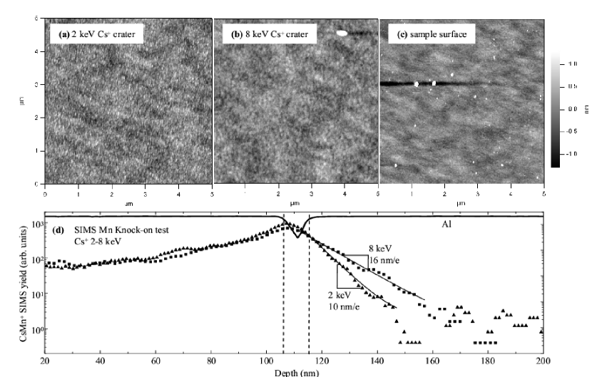
The Mn concentration profile for each sample is measured using SIMS and is plotted in Fig. 1(b) for a set of four 7.5-nm QWs grown on the same day at C with different Mn-doping levels. The primary beam consists of Cs+ ions with an impact energy of 2 keV providing a depth resolution of 3.25 nm/e, as calibrated using the atomically sharp AlGaAs/GaAs interface as a reference. The secondary ion used to measure the Mn concentration is CsMn+, which is resilient to changes in ionization yield at the AlGaAs/GaAs interface. The calibration of the SIMS Mn signal was performed using Mn-ion implanted GaAs as a reference, while the change in ionization yield of CsMn+ between AlGaAs and GaAs was checked using Mn-ion implanted AlGaAs reference samples. The z-axis calibration for the SIMS scans was performed using the Al signal as a reference for the QW region as well as the lower edge of the barrier, both layers grown at low temperature. The depth of the crater could not be used to calibrate the z-axis since it was found that the low temperature grown layers sputter faster than the high temperature grown buffer layers.
The Mn concentration peaks near the center of the QW region, as expected; but the surface side of the QW shows a large residual concentration of Mn which incorporates into the structure even after the Mn shutter has closed. Such behavior is not unexpected, even if the Mn-doping concentration is below the equilibrium solubility limit, since the growing surface is not at equilibrium. This behavior has previously been reported for similar structures in which Mn -doped GaAs grown at C showed large surface segregation.Nazmul:2003 We note that our results do not agree quantitatively with those of Nazmul et al, and we attribute this discrepancy to the different methods used for substrate temperature measurement in these two studies, noting that Mn incorporation is highly sensitive to this growth parameter. In our MBE system, the substrate temperature is measured directly by ABES, while an indirect temperature reading from a radiatively coupled thermocouple, used by Nazmul et al, can be more than C from the actual substrate temperature.
Mn surface segregation during growth may lead to Mn clustering in our samples and allow second phase magnetic precipitates, such as MnAs, to form. We note, however, that though these impurities are likely present in our samples, the schottky barrier around such precipitates prevents their detection in the electrical or optical signal of free carriers in the quantum wells. In the next section, the hole conductivity and carrier densities measured in these samples indicate, in comparison with the SIMS data, that most of the Mn impurities present in the sample are substitutionally incorporated. Thus Mn surface segregation and related growth defects have a negligible effect on our optical studies of the exchange splittings.
Below the QW, the Mn concentration decreases toward the substrate reaching a minimum point nm below the QW. The Mn profile is broader than the Al depth profile indicating either a SIMS mesurement artifact, such as poor depth resolution or preferential Mn sputtering, i.e. knock-on effects, or that Mn diffuses into the barrier. The lack of any temperature or doping level depedence on the Mn profile below the QW eliminates the latter possibility, while Mn knock-on effect has been reported in similar structure grown by Nazmul et al. To test for the presence of the knock-on effect, we run SIMS scans on the same sample (C) at two different beam energies, 2 keV and 8 keV, Fig. 2. Indeed, the Mn profile on the substrate side of the QW shows a beam energy dependence with a decay of 17 nm/e for 8 keV and 10nm/e at 2 keV. The Mn tail on the surface-side of the QW, where Mn incorporates as it floats along the surface, does not show any significant dependence on the beam energy. As a further test, we use an atomic force microscope (AFM) to measure the roughness of the SIMS craters for the 2 keV and 8 keV scans as 0.32 nm RMS and 0.30 nm RMS, respectively, while the roughness of the starting surface is 0.14 nm RMS. Since the crater roughness does not depend on beam energy, we conclude that the sample is uniformly sputtered at these two beam energies. Therefore, the observed difference in decay of the Mn profile is a result of the knock-on effect. Thus, the Mn profiles on the substrate side of the QW are sharper than the SIMS data show.
After the lower Mn tail, nm below the QW, the Mn profile becomes constant for all samples. Though the value of this background Mn concentration is near the detection limit of SIMS, it is seen to scale with Mn cell temperature as seen in Fig. 1(b). This behavior suggests that Mn flux escapes from the hot Mn cell and incorporates into the substrate even with the shutter closed. The Mn background for the control sample, grown with a cold Mn cell, is well below the SIMS detection limit.
III.2 Substrate temperature dependence
In Fig. 1(c), the Mn SIMS profiles are plotted for three 7.5-nm wide QWs grown with the same Mn cell temperature (same Mn beam flux), but different substrate temperatures. These SIMS scans were performed using an O2+ 2 keV beam. Note that the Mn profiles measured with the O2+ beam show a large sensitivity to AlGaAs/GaAs interfaces, probably due to oxygen impurities incorporated during growth in the AlGaAs layers, thus the vertical axis of these scans is uncalibrated (arbitrary units). The data, however, are qualitatively meaningful in the interface free regions, e.g. the top QW AlGaAs barrier.
As the substrate temperature is decreased, the Mn concentration profiles become dramatically sharper, the surface tail is eliminated, and the peaks become taller, indicating that, as expected, the Mn incorporation is energetically more favorable at lower temperature. Sharp Mn profiles, particularly on the surface side of the QW, are desirable for the engineering of more complex magnetic quantum structures in which a precise control of the magnetic doping is required. Optical signals, however, even at the relatively high growth temperatures of C and C, quench due to increased defect densities even in the non-magnetic control samples. Preliminary work shows that optical quality non-magnetic and magnetically doped InGaAs/GaAs QWs can be grown at C, suggesting that the loss in signal for the GaAs/AlGaAs QWs is related to Al, well-known for its impurity gettering of oxygen defects during MBE growth.Akimoto:1986 ; Achtnich:1987 Also noteworthy is a secondary peak in the Mn concentration 50 nm below the QW that occurs only in the C and C grown samples. This Mn peak corresponds to the interface between the high temperature and low temperature grown QW barrier, a point at which a long growth pause takes place. The peak indicates that the closed-shutter Mn flux, which scales with Mn cell temperature as discussed previously, may accumulate on the surface during the substrate cooling period before low temperature growth begins, and may subsequently incorporate once growth resumes, effectively delta doping the sample. In the C grown sample, grown on the same day and with the same Mn cell temperature, this effective delta doping does not occur, exemplifying the strong temperature dependence of Mn solubility in GaAs. Another possible explanation for this peak is that background impurities, such as oxygen, may incorporate during the long growth pause leading to a change in the SIMS ionization yield. This explanation is supported by the fact that the Al signal also shows a change in intensity at this same region even though the Al concentration should be constant.
III.3 The effective Managanese concentration
Since we probe carrier spin splittings at the band edges of the QWs, then the presence of Mn in the AlGaAs barriers does not directly interfere with our measurements. The leakage of Mn into the barriers, however, makes the determination of the effective Mn concentration in the QWs non-trivial. Since we are primarily interested in the measurement of the conduction band exchange parameter, we define the effective Mn concentration () in the QWs as the average of the SIMS concentration profile weighted by the electron probability density along the growth axis . is the square modulus of the ground state electron wave function calculated using a one-dimensional Poisson-Schroedinger solver.Snider:1 Thus, we calculate by numerical integration. and the corresponding values of are listed for a variety of QWs in Table 1. These values of are then used in the extraction of from time-resolved KR measurements.Myers:2005
As discussed previously, the decay of the Mn profiles on the substrate side of the QW is due to the knock-on effect, which is an artifact of the SIMS measurement.Therefore, the calculation of as discussed above contains this error. We estimate the uncertainty of by calculating the effective concentration assuming that the Mn profile on the substrate side of the QW is atomically sharp. Thus two values of are calculated for each sample from which we calculate a standard deviation in . These errors are generally %, except for the nm QW set in which the error reaches 15%. The errors lead to variations in our calculation of the exchange parameter, which are included in the error bars of these parameters (section VI).
| Sample | (∘C) | (nm) | (cm-3) | (cm-3) | (%) | Ea (meV) | ||
|---|---|---|---|---|---|---|---|---|
| A | 400 | 7.5 | 0.0065 | 0.71 | 0.90 | 68 | ||
| B | 400 | 7.5 | 0.0537 | 0.18 | 0.73 | 73 | ||
| C | 400 | 7.5 | 0.1266 | 0.15 | 0.72 | 96 | ||
| D | 400 | 3 | - | 0.0025 | - | 0.67 | - | |
| E | 400 | 3 | 0.0117 | 0.62 | 0.87 | - | ||
| F | 400 | 3 | 0.0274 | 0.56 | 0.85 | - | ||
| G | 400 | 10 | 0.0134 | 0.32 | 0.77 | 54 | ||
| H | 400 | 10 | 0.0310 | 0.31 | 0.77 | 41 | ||
| I | 400 | 10 | 0.0804 | 0.22 | 0.74 | 46 | ||
| J | 400 | 10 | 0.1274 | 0.16 | 0.72 | 59 | ||
| K | 400 | 5 | 0.0044 | 0.48 | 0.83 | - | ||
| L | 400 | 5 | 0.0110 | 0.61 | 0.87 | - | ||
| M | 400 | 5 | 0.0318 | 0.44 | 0.81 | 36 | ||
| N | 400 | 5 | 0.0574 | 0.32 | 0.77 | 47 | ||
| O | 350 | 7.5 | - | - | - | - | - | - |
| P | 325 | 7.5 | - | - | - | - | - | - |
| Q | 400 | 500 | 0.0610 | 0.16 | 0.72 | 71 | ||
| R | 400 | 500 | 0.2823 | 0.11 | 0.70 | 54 | ||
| S | 400 | 500 | 0.6292 | 0.02 | 0.67 | 53 |
III.4 Manganese incorporation versus well thickness
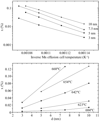
As discussed above, the Mn incorporation behavior in QWs is non-trivial, showing a peak in its concentration profile above the center of the well, and a strong dependence on substrate temperature. Under these circumstances, we expect a strong variation of the incorporation of Mn for wells of different widths under fixed Mn beam flux. The Mn concentration () is plotted in Fig. 3 (a) for four QW sample sets of varying width as a function of the inverse Mn effusion cell temperature. For each sample set of fixed width, the Mn concentration increases exponentially with Mn cell temperature indicating a linear relation between the Mn beam flux and doping density. For any given Mn cell temperature, however, the doping density decreases with QW width. This trend is explicitly plotted in Fig. 3 (b), where within each quantum well is plotted as a function of quantum well width for various Mn cell temperatures. This plot demonstrates that Mn incorporation is a strong function of well thickness for the growth conditions used here, particularly for high Mn beam fluxes (high effusion cell tempereatures).
The strong QW width dependence is likely due to the kinetics of Mn incorporation. These results are not surprising considering that many dopants do not imediately incorporate fully into semiconductors during MBE growth, e.g. In is well-known to only fully incorporate into GaAs once a critical density of In is deposited on the surface,Toyoshima:1993 for this reason sharp InGaAs/GaAs QWs are grown via predeposition of one monolayer of InAs followed by the alloy growth and subsequent reevaporation of the “In floating layer”.Nagle:1993 In this case, it is expected that narrow wells have lower total In densisties than wider wells, which is what we observe in the case of the GaMnAs QWs.
IV Hall effect
Measurements of carrier concentration are carried out at K on samples prepared in the Van der Pauw geometry and results are shown in Table 1. We examine carrier compensation related to As defects by comparing the electron density of a sample of 1 m of n-GaAs (Si-doped cm-3) grown in typical high temperature conditions (C) to that of a sample with the identical structure but grown at C, the same temperature as used for the Mn-doped QWs. In the C grown sample, the electron density is lower than in the C grown sample by cm-3, which provides an estimate for the compensation due to non-Mn related growth defects, i.e. excess As. Si incorporation is amphoteric which can lead to both n and p doping (Si self-compensation), however, for high temperature growth with Si doping level less than cm-3, we expect only n-type doping from Si.Macguire:1987 At lower temperature, Si may also act as an acceptor,Grandidier:1998 thus compensation assumed to be due to As defects could actually be occuring due to Si self-compensation leading to an overestimate of excess As. For this reason, the carrier compensation we observe in the C grown sample serves as an upper limit on the amount of excess As in our samples, cm-3, which is drastically smaller than the typical concentrations measured in low temperature (C) grown GaAs, cm-3.Missous:1994 We also note that the compensation threshold for our samples is lower than for ALE grown n-GaAs, cm-3 .Johnston:2003
IV.1 Manganese hole-doping calibration
Given, as discussed above, that growth defects not related to Mn-doping have a limited effect on the electronic properties for the chosen growth conditions, then the hole density in Mn-doped samples will be limited, for all practical purposes, only by the incorporation behavior of Mn. In order to determine the nature of Mn incorporation in our samples we investigate the p-doping dependence on Mn flux in a bulk calibration sample series grown under the same conditions as the Mn-doped QWs (C). These samples consist of 1 m of GaAs doped with Mn at various effusion cell temperatures. We plot sheet concentration of holes (p2D) per hour of Mn shutter time as a function of the inverse temperature of the Mn effusion cell in these samples (Fig. 4). The doping rate demonstrates exponential thermal activation, fitting well to an Arrhenius equation, which indicates that there is a linear relation between the Mn beam flux and the hole density. Thus, for this doping range and under these growth conditions, Mn incorporation is mostly substitutional. The hole densities for two additional sample sets, 15-nm and 30-nm GaMnAs QWs, are plotted in Fig. 4. Arrhenius fits to these data match the fit for the bulk sample set, which indicates that MnGa incorporation is sustained at these higher doping levels regardless of heterostructure effects. This is surprising considering that the effects of Mn penetration into the QW barriers and surface depletion could modify electrical properties, particularly for the narrower wells. The three-dimensional hole concentration () to ratio, , is listed in Table 1. Fruitful comparison of these values to those in typical GaMnAs (% and C) is difficult since GaMnAs usually contains orders of magnitude higher Mn and As defect concentrations than the samples discussed here.

IV.2 Manganese hole activation energy
In Fig. 5, the inverse sample temperature dependence of p2D for a sample set of 500-nm thick layers of bulk GaMnAs and for a sample set of 7.5-nm thick GaMnAs QWs are shown. At higher sample temperatures the activation energy () for holes is extracted from the linear portion of these plots, where the Mn-doped holes demonstrate clear exponential (Arrhenius) thermal activation. The Arrhenius behavior is maintained over a larger temperature range in the bulk than in the QWs, while at low temperature, carriers freeze out in both samples. In both bulk and QW samples, the linear portion of these plots decreases as the Mn concentration increases. Note that the linear fits to the data are carried out over smaller temperature ranges as increases. This behavior is expected to originate from the formation and broadening of the Mn acceptor band for large doping levels.

In Fig. 6, the activation energies for a number of bulk and QW samples are plotted as a function of Mn concentration. For all samples measured, we have observed an activation energy lower than the 110 meV reported in the literature for an isolated MnGa in GaAs.Yu:1979 This behavior was first observed in Mn doped GaAs by Blakemore et al, where the thermal activation energy of Mn acceptors was found to be below the optical ionization energy of 110 meV.Blakemore:1973 ; Woodbury:1973 The activation energies were lower than predicted due to impurity band broadening, suggesting a low energy pathway due to sample inhomogeneity. In the case of impurity band formation, we would expect a continued lowering of the activation energy with increased Mn-doping as the Mn acceptor level broadens into an impurity band, and eventually merges with the GaAs valence band above the insulator to metal transition. For our bulk GaMnAs samples, the activation energy does decrease with increased Mn doping, but for QWs this effect is perhaps masked by a strong variation of the temperature dependent hole concentration on QW width. For 3-nm wide QWs, reliable activation energy for holes could not be extracted since either p2D is not linear over any significant temperature range or the hall data are too noisy to be reliable. This behavior is also observed for the 5-nm wide QWs in which is only extracted for the two highest doping levels, but is not reliable for the two lowest Mn doped samples, whereas is reliably measured in all the 7.5-nm, 10-nm, and bulk 500-nm samples. The dependence on well thickness is probably due to carrier compensation from impurities, such as oxygen, that are gettered by Al during the growth of the AlGaAs QW barriers, discussed previously (see section IIIB). Barrier wave function penetration, and therefore barrier defect compensation, increases as the well width decreases.

V Substitutional Manganese Incorporation
An estimate of the fraction of Mn which is substitutionally incorporated can be made by assuming that each MnGa donates one free hole and each Mni compensates two holes.Erwin:2002 This calculation has recently been used in ferromagnetic GaMnAs () to estimate the concentrations of Mni and MnGa with respect to the crystal structure.Zhao:2005 Here we ignore As defect compensation since it is negligible under our chosen growth conditions ( cm-3). We also assume that charge compensation due to Mn-defects other than Mni (e.g. MnAs precipitates) are negligible. Thus, we write,
| (1) |
where is the concentration of substitutional Mn and is the concentration of interstitial Mn. Since is the sum of and , then we rewrite (1) in terms of ,
| (2) |
Values of this ratio are provided for each sample in Table I and plotted for four QW sample sets of varying doping density in Fig. 7. The observation of hole conduction in all Mn doped QWs provides a minimum value of , while the real value is expected to be larger since Eq. (1) ignores holes which cannot be measured due to the incomplete thermal activation of impurity bound holes at 300 K or surface depletion. For increased Mn-doping, the ratio decreases indicating that incorporation of growth defects, Mni or Mn-containing second phases such as MnAs, is becoming significant. Precipitates remove Mn from the lattice leading to a reduction in hole concentration relative to the purely substitutional case. Other forms of hole compensation such as interstitial-substitutional pairs Yu:2002 and dimers of two nearest neighbor substitutional MnRaebiger:2004 are unlikely to be present in our samples due to the low doping concentrations. Optical signals, predominantly PL, show a similar degradation with increased (see sections VI and VII). Note also, as indicated by the temperature dependence of the hole concentration, that particularly in the narrow QWs, and 5 nm compensation of holes due to barrier defects may also deflate our estimate of . Despite these factors the fraction of MnGa in all our samples is approximately 70-90% as shown in Fig. 7.

VI Time-Resolved Kerr Rotation
Electron spin dynamics are measured by time-resolved KR with the optical axis perpendicular to the applied magnetic field (Voigt geometry) and parallel to the growth direction . The measurement, which monitors small rotations in the linear polarization of laser light reflected off of the sample, is sensitive to the spin polarization of electrons in the conduction band of the QW.Crooker:1996 A mode-locked Ti:Sapphire laser with a 76-MHz repetition rate and 250-fs pulse width tuned to a laser energy near the QW absorption energy is split into a pump (probe) beam with an average power of 2 mW (0.1 mW). The helicity of the pump beam polarization is modulated at 40 kHz by a photo-elastic modulator, while the intensity of the linearly polarized probe beam is modulated by an optical chopper at 1 kHz for lock-in detection. Both beams are focused to an overlapping 50-m diameter spot on the sample which is mounted within a magneto-optical cryostat. The time delay between pump and probe pulses is controlled using a mechanical delay line. The pump injects electron spins polarized perpendicular to into the conduction band of the QW. The change in the probe polarization angle, is proportional to the average electron spin polarization in the QW and is well fit to a single decaying cosine, , where is proportional to the total spin injected, is the inhomogeneous transverse spin lifetime, is the electron spin precession (Larmor) frequency, and is the phase offset. No evidence of Mn2+ spin precession, which occurs in II-VI magnetically doped QWs,Crooker:1996 has been observed in the samples studied here. The order of magnitude smaller in our III-V QWs compared to the II-VI QWs puts any Mn2+ spin precession signal below the experimental detection limit.

Fig. 8(a) shows typical time-resolved KR data measured at T for a Mn-doped QW ( nm and ) together with fit, as described above, demonstrating electron spin coherence in the GaMnAs system. KR data showing electron spin precession was observed to quench in all samples for %.
VI.1 Transverse electron spin lifetime
The transverse electron spin lifetime () is plotted in Fig. 9 as a function of the percentage of Mn for all four QW sample sets. In all samples measured, we observe an increase in with Mn doping as compared to the un-doped control samples. This increase is consistent with the D’Yakonov-Perel (DP) spin relaxation mechanism since increasing impurity concentration makes the process of motional narrowing more efficient by providing additional momentum scatters.Fabian:1999 After reaching a maximum at very low Mn-doping (%), drops off as a function of as shown in Fig. 9. This behavior suggests that for %, the DP mechanism is no longer dominant. In this regime either the Elliot-Yafet (EY) or the Bir-Aronov-Pikus (BAP) relaxation mechanisms may limit conduction electron spin lifetimes, since both should increase in strength with increasing .Optical:1984 EY relaxation, due to the spin-orbit interaction, grows stronger with larger impurity concentration while, the BAP process, based on the electron-hole exchange interaction, increases with increasing hole doping.
In this discussion we have so far ignored the effects of the exchange interaction on the electron spin relaxation process. In II-VI DMS, the presence of magnetic impurities leads to large relaxation rates limiting the conduction electron spin lifetime. Crooker:1996 Magnetic impurity doping in these materials results in relaxation through spin-flip scattering arising from the exchange interaction. While the samples discussed in this report have exchange energies which are several orders of magnitude smaller than in typical II-VI DMS, the effect of magnetic interactions on cannot be totally ruled out. Several experiments can be carried out in order to examine the role of exchange interactions in the decoherence of electron spin including a finer dependence of on and a dependence on the temperature. A detailed study of changes in as a function of QW width also may discern between the DP and the exchange scattering mechanism.Semenov:2003 Such detailed studies will be the subject of future work. Finally we note that qualitatively similar dependence of on Mn-doping as shown in Fig. 9 has recently been observed in InGaMnAs/GaAs QWs.Unpublished:1

VI.2 Larmor precession frequency
is proportional to the total conduction band spin splitting between spin-up and spin-down electrons () and can be expressed in terms of the Zeeman splitting (), and the exchange splitting ():
| (3) |
Here is Planck’s constant, is the in-plane electron g-factor, is the Bohr magneton, and is the component of Mn2+ spin along . , where is the spin-5/2 Brillouin function, is the g-factor for Mn2+, is Boltzman’s constant, and is the paramagnetic Curie temperature. Note that since the g-factor for Mn2+ () is positive, for , then . We emphasize that a measurement of alone, because of phase ambiguity, does not determine the sign of .
In Fig. 8(b), is plotted as a function of for a set of four samples with nm and varying . The non-magnetic () sample shows a linear field dependence of , from which we extract values of as described in Eq. (3). As the Mn doping concentration is increased, increases and its dependence becomes non-linear. Further, this field dependence shows the same Brillouin function behavior that is expected for the magnetization of paramagnetic GaMnAs, Eq. (3). The dependence of on and for the sample with nm and is plotted in Fig. 10(a) and (b) together with values for the control sample, and nm. For the magnetic sample, as is increased, decreases asymptotically toward the control sample value without crossing zero (Fig. 10(a)). Thus, it follows from Eq. (3) and from the sign of that for nm, has the same sign as . For nm, ,Snelling:1991 and thus . This conclusion is also supported by the QW width dependence discussed below.

Using extracted from the sample (green line) and Eq. (3) we fit data as a function of and to,
| (4) |
which has only two fit parameters, and . Comparing Eqs. (4) to (3), it is clear that . The data in Fig. 8(b) and Fig. 10 are fit to Eq. (4), with fits shown as red lines. A large negative (-24 K) is extracted from the fits for the sample with the lowest Mn doping (Fig. 10), which may be explained by an increased spin temperature of Mn2+ due to photoexcitation. This effect has been reported in II-VI DMS for low magnetic doping levels.Keller:2001 Also supporting this hypothesis, we find smaller values of ( K) in samples with larger .

is examined in detail for QWs of varying . For this analysis, we examine four sets of samples with various (including ) for and nm. Note that each sample set of constant was grown on the same day, which we have observed to reduce QW thickness variations between samples within each set from % to %. Variations in QW thickness can affect the electron g-factor and therefore result in errors in the determination of . By growing samples on the same day, the error in the determination of is reduced from 10% to less than 3% as compared with samples grown on different days. In Fig. 11, in the non-magnetic () QWs is plotted as a function of together with data from two other publications.Snelling:1991 ; Poggio:2004 Our data track the thickness dependence of the QW g-factor as previously reported with a slight positive shift in . The larger Al concentration (40%) in the QW barriers used in our samples versus the concentration (33%) used in Refs. Snelling:1991 ; Poggio:2004 accounts for this discrepancy.Weisbuch:1977 Knowing the absolute sign of for QWs of any width, we determine the sign of for each in the manner described previously. With a calibrated sign, is plotted in Fig. 12 as a function of for all four QW sample sets with varying . As shown in Fig. 12, for any given , decreases as increases.

Following from Eq. (3) and from the sign of , this demonstrates that is negative, i.e. antiferromagnetic, which has been reproduced unambiguously in over 20 additional samples. A negative has also been measured in recent time-resolved FR measurements in InGaMnAs/GaAs QWs.Unpublished:1
The effect of increasing temperature on the dependence of for the nm and sample is shown in Fig. 13, which dramatically illustrates the negative constant. For nm, is weakly positive, thus for and at high temperature . As the temperature descreases, becomes more negative as the paramagnetic susceptibility increases. At K and T, since the exchange splitting is equal and opposite to the Zeeman splitting. For lower temperature, since . We note that the data are well fit to Eq. (4) despite their highly non-linear nature. We contrast our observation of antiferromagnetic exchange in III-V GaMnAs, with the ferromagnetic exchange ubiquitous in II-VI DMS. In those systems symmetry forbids hybridization of and orbitals, such that only direct (ferromagnetic) exchange is possible.Larson:1988 The antiferromagnetic exchange in GaMnAs may be due to the narrower band gap of this material compared with II-VI, such that the conduction band has partial p-character thus allowing hybridization with the d orbitals localized on the Mn2+ impurities.

In Fig. 14, the fit parameter is plotted as a function of together with linear fits for each sample set of constant . The finite values of at , extrapolated from the linear fits, are attributed to either the experimental error in the determination of in the non-magnetic QWs or error in the measurement of , both of which have a negligible effect on the slope. These linear fits demonstrate that is constant over the measured doping range for QWs with the same width, but it varies with as plotted in Fig. 15(a). is more negative the narrower the QW, while it appears to saturate for wide QWs. In II-VI DMS QWs, a negative change in as large as meV was previously reported for increasing confinement and was attributed to a kinetic exchange coupling due to the admixture of valence and conduction band wave functions.Merkulov:1999

We plot as a function of the electron kinetic energy () in Fig. 15(b), and the data are linear. Here, is defined as the energy between the bottom of the conduction band in the GaAs QW and the ground state energy, which is calculated using a one-dimensional Poisson-Schroedinger solver and the material and structural parameters of the QWs.Snider:1 Extrapolating to we obtain a bulk value of meV for GaMnAs. A change in as large as meV is observed in the narrowest wells measured ( nm) and the slope of is roughly the same as reported by Merkulov et al. in II-VI DMS. Since in bulk II-VI DMS, the kinetic exchange effect appears as a reduction of , and is expected to cross through zero for very large confinement. Rather than a reduction, we observe an increase in in GaMnAs QWs. This observation is consistent with the predicted negative contribution of the kinetic exchange, since we measure in our samples.

is observed to be negative for all the samples studied here indicating that either long range Mn-Mn coupling is antiferromagnetic or the Mn2+ spin temperature is larger than the lattice temperature. Preliminary studies on modulation p-doped structures indicate that the negative is due to a combination of Mn2+ spin heating by photoexcitation, as previously discussed, and the lack of strong hole-mediated ferromagnetic Mn-Mn interaction, which occurs for much larger . In our samples the mean Mn-Mn distance may be too long for hole-spin coherence to be maintained, thus precluding long-range ferromagnetic coupling.
Note that the magnetization of the Mn acceptors depends on their electronic structure. Mn acceptors in GaAs can exist in either the ionized (Mn2+) configuration such that and , or as a neutral complex consisting of the same core with a loosely bound S=3/2 hole antiferromagnetically coupled to it; for this entire complex and .Schneider:1987 Though found in GaP,Kreisel:1996 the fully bound state with has never been observed in GaAs. and have different angular momentum states and thus give rise to different bulk magnetizations as measured with a SQUID, for instance. The spin state of the core electrons (), however, remains unchanged. Since exchange involves the interaction between electrons in the conduction band and electrons of the Mn-ion, the value of should remain unchanged regardless of the presence of the loosely bound hole.Szczytko:1999 In contrast, exchange is strongly modified by this hole. The presence of a loosely bound hole in the neutral complex opens a ferromagnetic exchange path whereas the ionized acceptor offers only antiferromagnetic channels. In the literature, such a dependence on the nature of the Mn acceptor core is offered as an explanation for the apparent sign flip of the term as the Mn concentration was increased from the very dilute limit (paramagnetic) to the high doping regime (ferromagnetic). It may also explain the widely varying values of measured in our PL experiments (section VII). We emphasize that our exchange splitting model takes and thus neglects any effect of the loosely bound hole on the core state g-factor since the exchange interaction between the hole and the core is expected to be small.Linnarsson:1997 Measurements in III-V DMS support this assumption by consistently showing = 2.0. Therefore, the relative concentration of and centers in our samples should have a negligible effect on both and , allowing us to ignore this detail in our extraction of from the data.
VII Photoluminescence
Since hole spin lifetimes are very short in GaAs QWs ( ps), we rely on measurements of PL to shed light on the -like valence band and its magnetic coupling to Mn-bound electrons, . In addition, because recombination happens near impurities, PL can reveal important information on defects and magnetic doping. Polarization-resolved PL is measured as a function of in the Faraday geometry with PL collected normal to the sample surface. The excitation laser is linearly polarized and focused to a spot 100 m in diameter with an energy set above the QW absorption energy. While PL is seen to quench with increasing Mn doping, as seen in Fig. 16, QWs with or with small emit PL whose energy dependence is well fit by two Gaussians (Fig. 17). The emission energy of the narrower, higher-energy Gaussian peak tracks the dependence expected for the Zeeman splitting in QWs, indicating that this peak is due to heavy hole exciton recombination. On the other hand, the wider, lower-energy Gaussian is likely due to donor-bound exciton emission from shallow donors in the QWs. These shallow donors are likely Mni, since the emission linewidth increases as the calculated Mni concentration increases. Though the lower energy Gaussian is the result of Mn doping, it is also present in some non-magnetic samples grown with a cold Mn cell (Fig. 17), perhaps due to an impurity level of Mni ( cm-3).

In addition to quenching the PL, increased Mn-doping broadens the low-energy emission peak. Fig. 16 shows the zero field PL emission at K for 7.5-nm wide QWs of varying Mn-doping. The effect of increasing Mn-doping is qualitatively identical for all QWs of varying width: 3.0, 5.0, 7.5, and 10.0 nm. As doping increases, the PL broadens in energy, red shifts, and decreases in intensity, eventually quenching. The decreasing intensity of the PL with increasing Mn-doping parallels the degradation in KR signal with Mn-doping. The degradation of these two optical signals, each with distinct physical origins, i.e. emission and absorption, reflects the increasing density of crystalline defects with Mn-doping.

VII.1 Zeeman splitting
The splitting in the polarized emission energy of the higher energy Gaussian, , is measured in all the non-magnetic samples. For small fields ( T), depends linearly on field with the slope giving the out-of-plane heavy hole exciton g-factor (). The extracted values of agree within the experimental error with previously published values.Snelling:1992 At higher fields, deviates from linearity, particularly in the wider QWs as shown in Fig. 18(a) and (b) where it reverses sign in both the 10-nm and the 7.5-nm QWs for at T.

In Mn-doped samples, results from both the Zeeman splitting () and the exchange splitting ():
| (5) |
Using the measurements of from the samples and the previously extracted values of and at K (Fig. 12), we fit to Eq. (5). In the 10-nm QW for low fields we estimate eV using the fits shown in Fig. 18(a) as blue lines. As Fig. 18(a) makes clear, this model breaks down at high fields where non-linearities dominate .
Similar non-linear behavior in at high fields in the 7.5-nm QWs, as shown in Fig. 18(b), contributes to the large uncertainty in our estimates of . Further complicating the determination of are the widely differing values extracted for samples of different widths. Using fits shown in Fig. 18, we find , , and eV for QWs with 7.5, 5.0, and 3.0 nm, respectively. Such dissagreement between samples indicates the incompleteness of our model for the valence band; the mixing of valence band states may be contributing to the problematic extraction of the exchange coupling especially for small .Snelling:1992 Clearly, more work is necessary for the determination of in GaMnAs QWs and its dependence on . Previous measurements in bulk GaMnAs provide little guidance with one report suggesting positive exchange for low (paramagnetic) Szczytko:1996 , and others finding negative exchange for much larger (ferromagnetic) Matsukura:1998 ; Okabayashia:1998 ; Zudov:2002 .
VII.2 Photoluminescence polarization
We compare the PL polarization spectra of the 7.5-nm QW with % with the well-known Mn-acceptor emission line in bulk GaAs at 1.4 eV (Fig. 19(a) and (b)).Yu:1979 PL polarization is defined here as . The bulk Mn-acceptor line, shown in Fig. 19(b), is measured in the same sample, resulting from the unintentional doping of Mn in the 300-nm GaAs buffer layer grown below the QW structure; the SIMS profiles in Fig. 1 show that the Mn concentration in this layer is less than cm-3. The polarization of this peak demonstrates a paramagnetic (Brillouin function) field dependence, shown in Fig. 19(d), following the magnetization of the MnGa acceptors in the bulk GaAs. The low-energy peak in the QW PL polarization coincides with the low-energy PL peak which we assigned to emission from Mni donor bound excitons. Its polarization is plotted in Fig. 19(c) (solid points) and demonstrates similar paramagnetic (Brillouin function) behavior with field and temperature to that of the bulk Mn-acceptor line.

The polarization of the bulk Mn-acceptor line is proportional to the spin-polarization of local Mn2+ moments since the PL from this line results from conduction band electrons recombining with holes trapped on MnGa acceptors. The spin of these holes is coupled to the local Mn2+ spin.Petrou:1985 We postulate a similar mechanism for the low-energy polarization feature in the QW PL in which holes in the valence band of the QW recombine with electrons bound to Mni donors. The clear Brillouin-like field dependence indicates that the recombinant polarization originates around isolated paramagnetic Mn impurites in the lattice, i.e. either MnGa acceptors or Mni donors. The Brillouin-like behavior is inconsistent with coupled Mn centers such as interstitial-substitutional pairs, which couple antiferromagnetically and which are unlikely to be present in samples with such low Mn content.Yu:2002 The meV redshift of the polarization peak from the main QW peak does not match the 110 meV binding energy of the substitutionial acceptor. While there is an excited state of the MnGa acceptor with a binding energy of 26 meV,Lakshmi:2004 recombination from this excited state is unlikely when each acceptor is filled with, at most, one hole and given that PL usually originates from the lowest available energy levels. Rather, we assume that the recombination originates from the Mni donor and the valance band in the QW. Comparison to the experimentally measured Mni donor binding energy is not possible since none are reported. The postulated coupling of the electron spin to Mni spin results in polarized emission which follows the magnetization of Mni within the QW. These measurements open the possibility of indirectly measuring the magnetization of the Mn impurities in the QWs using polarization-resolved magneto-PL.
The high-energy feature in the QW PL polarization involves recombination of electrons and holes bound to the QW, but delocalized relative to the Mn states. Due to the exchange interactions in both the valence and conduction band, the spin splitting, and thus the resulting polarization, should have a Brillouin function field dependence Eq. (5). For the small values of studied here, however, these effects are not resolvable and the polarization shows a weaker field dependence Fig. 19(c) (open points) with an opposite sign compared to the polarization of the low-energy peak (solid points).
VIII Conclusions
In summary, we demonstrate the growth of III-V GaMnAs based heterostructures in which coherent electron spin dynamics and PL can be observed. By lowering the substrate temperatures during growth, sharper Mn profiles and higher Mn concentrations are attained, however optical signals eventually quench (C) likely due to incorporation of defects by Al gettering, such as oxygen. Optical signals are also seen to quench for %. Hole doping due to substitutional Mn incorporation is sensitive to the quantum well width indicative of compensation by defects in the AlGaAs barriers. The activation energy of holes in the QWs is lower than for an isolated substitutional Mn in GaAs providing evidence for impurity band formation and broadening due to large Mn doping. The crystallographic incorporation behavior is estimated from the SIMS and Hall data and we find that for all samples studied at least 70-90% of Mn is located on substitutional Ga sites. The exchange induced spin splitting in the conduction band in the GaMnAs QWs matches the traditional paramagnetic DMS picture and allows for the determination of the exchange parameter via time-resolved electron spin spectroscopy. Suprisingly the measured exchange coupling is antiferromagnetic in GaMnAs QWs, a result not predicted by current DMS theories. No evidence of long-range Mn spin coupling is observed, but negative effective Curie temperatures indicate spin heating of the Mn sublattice by photoexcitation. Electron spin lifetimes in the QWs increase for the lowest Mn dopings compared with undoped samples indicating the dominance of the Dyakanov-Perel mechanism over spin-flip scattering in this regime. The ability to magnetically dope III-V and maintain sensitive optical properties opens the door for more complex structures to be used in the study of both free carrier and magnetic ion spin at fast time scales, a technology which was previously limited to II-VI DMS.
Acknowledgements.
The authors thank T. Mates (MRL, UC Santa Barbara) and Charles Evans and Associates for SIMS measurements, J. H. English and A. W. Jackson for MBE technical assistance, and J. Miller (Smelrose Institute) for entertaining discussions. This work was financially supported by DARPA, ONR, and made use of MRL Central Facilities supported by the MRSEC Program of the National Science Foundation under award No. DMR00-80034. One of us (N. P. S.) acknowledges the support of the Fannie and John Hertz Foundation.References
- (1) H. Ohno, A. Shen, F. Matsukura, A. Oiwa, A. Endo, S. Katsumoto, and Y. Iye, Appl. Phys. Lett. 69, 363 (1996).
- (2) T. Dietl, H. Ohno, and F. Matsukura, Phys. Rev. B 63, 195205 (2001).
- (3) H. Ohno, J. Magn. Magn. Mater. 272, 1–6 (2004).
- (4) A. H. Macdonald, P. Schiffer, and N. Samarth, Nature Materials 4, 195-202 (2005).
- (5) T. Dietl, (Diluted) Magnetic Semiconductors, in Handbook of Semiconductors, (ed. S. Mahajan) Vol.3B (North-Holland, Amsterdam, 1994), p. 1251.
- (6) M. J. Snelling, G. P. Flinn, A. S. Plaut, R. T. Harley, A. C. Tropper, R. Eccleston, and C. C. Phillips, Phys. Rev. B 44, 11345 (1991).
- (7) M. J. Snelling, E. Blackwood, C. J. McDonagh, and R. T. Harley, Phys. Rev. B 45, 3922 (1992).
- (8) N. J. Traynor, R. T. Harley, and R. J. Warburton, Phys Rev. B 51, 7361 (1995).
- (9) Y. K. Kato, R. C. Myers, A. C. Gossard, and D. D. Awschalom, Science 306, 1910 (2004).
- (10) G. Salis, Y. Kato, K. Ensslin, D. C. Driscoll, A. C. Gossard and D. D. Awschalom, Nature 414, 619 (2001).
- (11) Y. Kato, R. C. Myers, D. C. Driscoll, A. C. Gossard and D. D. Awschalom, Science 299, 1201 (2003).
- (12) M. Poggio, G. M. Steeves, R. C. Myers, N. P. Stern, A. C. Gossard and D. D. Awschalom, Phys. Rev. B 70, 121305(R) (2004).
- (13) Y. Kato, R. C. Myers, A. C. Gossard, and D. D. Awschalom, Nature 427, 50 (2004).
- (14) Y. K. Kato, R. C. Myers, A. C. Gossard, and D. D. Awschalom, Phys. Rev. Lett. 93 176601 (2004).
- (15) S. A. Crooker, D. D. Awschalom, J. J. Baumberg, F. Flack, and N. Samarth Phys. Rev. B 56, 7574 (1997); S. A. Crooker, J. J. Baumberg, F. Flack, N. Samarth, D. D. Awschalom, Phys. Rev. Lett. 77, 2814 (1996).
- (16) R. C. Myers, K. C. Ku, X. Li, N. Samarth, and D. D. Awschalom, Phys. Rev. B 72, 041302(R) (2005).
- (17) E. Johnston-Halperin, J. A. Schuller, C. S. Gallinat, T. C. Kreutz, R. C. Myers, R. K. Kawakami, H. Knotz, A. C. Gossard, and D. D. Awschalom, Phys. Rev. B 68 165328 (2003).
- (18) R. C. Myers, A. C. Gossard, D. D. Awschalom, Phys. Rev. B 69, 161305(R) (2004).
- (19) Unpublished result.
- (20) R. C. Myers, M. Poggio, N. P. Stern, A. C. Gossard, and D. D. Awschalom, Phys. Rev. Lett. 95, 017204 (2005).
- (21) K. Wagenhuber, H-P Tranitz, M. Reinwald, and W. Wegscheider, Appl. Phys.Lett. 85, 1190 (2004).
- (22) A. M. Nazmul, S. Sugahara, and M. Tanaka, J. Crys. Grow. 251, 303 (2003).
- (23) K. Akimoto, M. Kamada, K. Taira, M. Arai, and N. Watanabe, J. Appl. Phys. 59, 2833 (1986).
- (24) T. Achtnich, G. Burri, M. A. Py, and M. Ilegems, Appl. Phys. Lett. 50, 1730 (1987).
- (25) 1D Poisson-Schroedinger solver written by G. Snider, (http://www.nd.edu/ gsnider/).
- (26) H. Toyoshima, T. Niwa, J. Yamazaki, and A. Okamoto, Appl. Phys. Lett. 63, 821 (1993).
- (27) J. Nagle, J. P. Landesman, M. Larive, C. Mottet, and P. Bois, J. Cryst. Growth 127, 550 (1993).
- (28) J. Maguire, R. Murray, R. C. Newman, R. B. Beall, and J. J. Harris, Appl. Phys. Lett. 50, 516 (1987).
- (29) B. Grandidier, D. Sti venard, J. P. Nys, and X. Wallart, Appl. Phys. Lett. 72, 2454 (1998).
- (30) M. Missous and S. O’Hagan, J. Appl. Phys. 75, 3396 (1994).
- (31) P. W. Yu and Y. S. Park, J. Appl. Phys. 50, 1097 (1979).
- (32) J. S. Blakemore, Winfield J. Brown, Jr., Merrill L. Stass, and Dustin A. Woodbury, J. Appl. Phys. 44, 3352 (1973).
- (33) D. A. Woodbury and J. S. Blakemore, Phys. Rev. B 8, 3803 (1973).
- (34) S.C. Erwin and A.G. Petukhov, Phys. Rev. Lett. 89, 227201 (2002).
- (35) L. X. Zhao, C. R. Staddon, K. Y. Wang, K. W. Edmonds, R. P. Campion, B. L. Gallagher, and C. T. Foxon, Appl. Phys. Lett. 86, 071902 (2005).
- (36) K. M. Yu, W. Walukiewicz, T. Wojtowicz, I. Kuryliszyn, X. Liu, Y. Sasaki, J. K. Furdyna, Phys. Rev, B 65, 201303(R) (2002).
- (37) H. Raebiger, A. Ayuela, and R. M. Nieminen, J. Phys.: Condens. Matter. 16, L457 (2004).
- (38) J. Fabian and S. das Sarma, J. Vac. Sci. Technol. B 17, 1708 (1999).
- (39) Optical Orientation, Modern Problems in Condensed Matter Science, edited by F. Meier and B. P. Zachachrenya (North-Holland, Amsterdam, 1984), Vol. 8.
- (40) Y. G. Semenov, Phys. Rev. B 67, 115319 (2003).
- (41) D. Keller, D. R. Yakovlev, B. Konig, W. Ossau, Th. Gruber, A. Waag, and L. W. Molenkamp, Phys. Rev. B 65, 035313 (2001).
- (42) C. Weisbuch and C. Hermann, Phys. Rev. B 15, 816 (1977).
- (43) B. E. Larson, K. C. Hass, H. Ehrenreich, and A. E. Carlsson, Phys. Rev. B 37, 4137 (1988).
- (44) I. A. Merkulov, D. R. Yakovlev, A. Keller, W. Ossau, J. Heurts, A. Waag, G. Landwehr, G. Karczewski, T. Wojtowicz, and J. Kossut, Phys. Rev. Lett. 83, 1431 (1999).
- (45) J. Schneider, U. Kaufmann, W. Wilkening, M. Baeumler, Phys. Rev. Lett. 59, 240 (1987).
- (46) J. Kreisel, W. Ulrici, Phys. Rev. B 54 10508 (1996).
- (47) J. Szczytko, W. Mac, A. Twardowski, F. Matsukura, H. Ohno, Phys. Rev. B 59, 12935 (1999).
- (48) M. Linnarsson, E. Janzen, B. Monemar, M. Kleverman, A. Thilderkvist, Phys. Rev. B 55, 6938 (1997).
- (49) J. Szczytko, W. Mac, A Stachow, A Twardowski, P. Becla, and J. Tworzydlo, Solid State Commun. 99, 927 (1996).
- (50) F. Matsukura, H. Ohno, A. Shen, and Y. Sugawara, Phys. Rev. B 57, 2037(R) (1998).
- (51) J. Okabayashia, A. Kimura, O. Rader, T. Mizokawa, A. Fujimori, T. Hayashi, and M. Tanaka, Phys. Rev. B 58, R4211 (1998).
- (52) M. A. Zudov, J. Kono, Y. H. Matsuda, T. Ikaida, N. Miura, H. Munekata, G. D. Sanders, Y. Sun, and C. J. Stanton, Phys. Rev. B 66, 161307(R) (2002).
- (53) A. Petrou, M. C. Smith, C. H. Perry, J. M. Worlock, J. Warnock, and R. L. Aggarwal, Sol. State Commun. 55, 865 (1985).
- (54) B. Lakshmi, G. Favrot, D. Heiman, Proc. SPIE 5359, 290 (2004).