Tunneling spectroscopy studies of aluminum oxide tunnel barrier layers
Abstract
We report scanning tunneling microscopy and ballistic electron emission microscopy studies of the electronic states of the uncovered and chemisorbed-oxygen covered surface of AlOx tunnel barrier layers. These states change when chemisorbed oxygen ions are moved into the oxide by either flood gun electron bombardment or by thermal annealing. The former, if sufficiently energetic, results in locally well defined conduction band onsets at 1 V, while the latter results in a progressively higher local conduction band onset, exceeding 2.3 V for 500 and 600 C thermal anneals.
pacs:
73.40.Gk, 73.61.Ng, 85.25.Cp, 68.37.Ef, 85.75.DdThe prevalence of aluminum oxide layers formed by room temperature oxidation as the barrier in Josephson junctions (JJ)Gurvitch et al. (1983) and magnetic tunnel junctions (MTJs)Moodera et al. (1995) continues to motivate efforts to better understand and control its electronic structure. While bulk, stoichiometric Al2O3 has a band gap of 8.8 eV,French (1990) for amorphous AlOx films grown at 20 C it is a much smaller. This is beneficial as thin, transparent barriers provide the high critical current densities (JJs) and low specific impedance levels (MTJs) required by many applications, but band tails, localized states, and spatial inhomogeneities that may also be found in amorphous AlOxPlisch et al. (2001); Rippard et al. (2002); Perrella et al. (2002) can be very detrimental for high performance, low noise applications.Zhang and White (1998); Tsymbal and Pettifor (1998) Indeed, conducting atomic force microscopy studies of AlOx layers have shown inhomogeneous current distributions at the nanoscale, attributed to either a variation in local barrier heightsAndo et al. (2000) or in barrier thicknessLuo et al. (2001). However, a serious challenge for such surface spectroscopy studies of the electronic properties of AlOx is that the surface is invariably covered, even in ultra-high vacuum (UHV), with chemisorbed oxygen bound by positively charged oxygen vacancies in the oxide, with the degree of coverage depending on oxide thickness.Perrella et al. (2002); Tan et al. (2005)
We report the use of scanning tunneling microscopy (STM) and ballistic electron emission microscopy (BEEM) to examine the density of states (DOS) of the AlOx surface, and to determine how these states change when chemisorbed oxygen ions are moved into the oxide by either flood-gun electron-bombardment (FGEB), or by thermal annealing. Both treatments greatly reduce, if not eliminate, low energy band tail states and narrow the DOS distribution over an oxide area. However FGEB, which we argue has similarities in effect to depositing a metallic over-layer with a high work function , causes different changes in the DOS than annealing. The former, if sufficiently energetic, results in locally well defined conduction band onsets at 1 V, while the latter results in a progressively higher local conduction band onset, exceeding 2.3 V for 500 and 600 C anneals.
We fabricated the samples for this study via thin film thermal evaporation and post-growth processing in UHV. For most samples, we deposited 12 nm of Au on hydrogen terminated (111) Si to form a high quality Schottky barrier (SB) to serve as the BEEM detector. This was followed by a 1.2 nm buffer layer of Cu, 1.2 nm Co, and finally 1 nm Al, which was oxidized by a 10 torr-sec exposure to oxygen (99.9985 % purity). X-ray photoemission (XPS) measurements show that this exposure forms a 1 nm AlOx layer. Some samples were then annealed in UHV while others were subjected to FGEB. Upon completion of processing, the sample was vacuum transferred to an adjacent UHV chamber for STM and BEEM measurements. Samples that were annealed at T 500 C had the Au/Cu/Co underlayers replaced with a single Co 20 nm layer to avoid Au diffusion into the Si. No BEEM measurements were made on those samples.
Scanning tunneling spectroscopy (STS) studies of aluminum oxide barrier layers are challenging because of both the chemisorbed oxygen discussed above and the propensity of the tunneling current to locally degrade the oxide via hot electron effects. It was shown earlierPerrella et al. (2002) that BEEM measurements, in conjunction with STS, can distinguish between where the STM is tunneling to the chemisorbed oxygen that is stabilized into nanoscale clusters by a local maximum in the vacancy concentration, and where the STM is tunneling to the bare oxide surface. In the former case, at sufficiently high tip bias, the electrons tunnel predominately into oxygen-cluster states, from which they eventually exit to the underlying metal via an inelastic process, resulting in no discernable BEEM signal. In the latter case, due to a low density of extended states on the oxide, the STM tip must approach close enough to establish feedback that there is substantial tunnel current directly through the oxide layer to the base electrode. Thus, a fraction of the tunnel-injected electrons travel ballistically to and across the underlying SB if they have the requisite energy and momentum values. The result for untreated, oxidized samples is BEEM spectra that are the same in form but reduced in amplitude from those obtained from unoxidized samples.
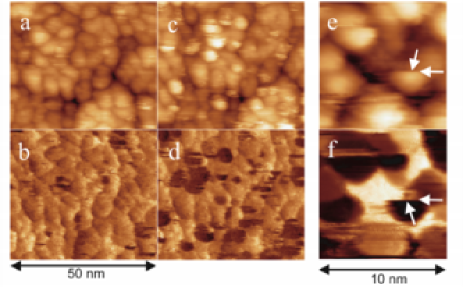
BEEM is also effective in detecting degradation of the oxide layer due to electrical stress during STM studies. The primary effect of prolonged and/or high current STM measurement over a small region of the surface is to partially reduce the oxide, generating positively charged oxygen vacancies, which can locally stabilize a nanocluster of chemisorbed O on the surface. This is readily detected by BEEM if the surface is scanned at high enough bias that the tunneling is to unoccupied states. Fig. 1 (a) and (b) are initial topographic and BEEM images taken on the surface of an un-annealed sample and show a low density of chemisorbed clusters; dark regions in the BEEM scan correlated with elevated regions in the topography. Subsequent scans, e.g. Fig. 1 (c) and (d), reveal a stress-induced accumulation of such clusters. These stress effects which can cause the motion of a cluster to a more stable position as oxygen vacancies are generated under the tip, require that STS on the uncovered surface be taken only for a short time and with a low tunneling current, impacting both the STS signal-to-noise and the ability to systematically survey the oxide surface. Fig. 1 (e) and (f) show images of a thermally annealed sample (3 min at 375 C). While the un-annealed sample accumulates an increasing number of clusters with scanning time, annealed samples exhibit only the motion of an approximately constant density of clusters, demonstrating that the annealed oxide is resistant to STM stress effects.
Using BEEM to determine locations where the tunneling is to the uncovered oxide surface, STS and BEEM measurements were made on the as grown oxide, and after different surface processing procedures. Fig. 2 shows typical results of the differential logarithmic conductivity, , proportional to the local DOS of the surface, together with the BEEM spectrum, . The tip was held steady during measurement, with 1 nm lateral drift, and 20 scans were averaged. As illustrated in Fig. 2a, the uncovered, as-formed AlOx surface yields DOS curves with a nearly parabolic dependence on bias extending to within 150 mV of the Fermi level E. While the details of the local DOS varied across the uncovered oxide, at no location was the DOS onset higher than 200 mV.
However, the STS is not indicative of the electronic structure of the oxide when it is embedded in a tunnel junction structure via over-coating with an electrode. An XPS studyTan et al. (2005) has found that this drives much of the chemisorbed oxygen into the oxide, filling oxygen vacancy sites and presumably substantially altering the electronic character of the tunnel barrier layer. A strong, positive correlation was found between the increase in oxygen content and the work function difference between top and bottom electrodes. This is consistent with the finding that negatively charging the surface via FGEB can also drive some or all of the chemisorbed oxygen into the oxide, depending upon the bias and exposure time.
To determine the effect of filling oxide vacancies on the electronic structure of AlOx layers, samples were subjected to FGEB and then examined by STS and BEEM. Samples were subjected to either 10 V or 20 V FGEB at a current density of 20 /cm2 for 2 hours. The 10 eV sample was dosed again (300 torr-sec), and bombarded a second time, which further stabilizes oxygen in the AlOx barrier.Tan et al. (2005)
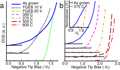
As illustrated in Fig. 2a, the effect of FGEB on the electronic properties of the oxide was profound. After the 10 V treatment STS measurements on the uncovered oxide surface showed no detectable oxide states from 0 (Ef) to 0.5 V, with a roughly parabolic energy dependence above 0.5 V. The details of the DOS varied slightly with location, but at no point was the onset either lower than 0.35 V or higher than 0.65 V. However, due to the inability of the STS measurements to completely survey the oxide surface and to the limited sensitivity of the measurement, we cannot rule out a small density of remnant low energy states in the oxide. STS measurements made with both positive and negative tip bias showed that the local DOS is roughly symmetric about V = 0, indicating that the Fermi level is pinned near the center of the oxide band-gap for these AlOx layers.
For the 20 V FGEB the region of zero DOS increased further to approximately 1.1 V, above which the DOS increased rapidly, as shown in Fig. 2a. A notable feature of the 20 V sample was that it was particularly quick to degrade; forming chemisorbed oxygen clusters shortly after we began examining a region with STM, indicating that when oxygen has been forcefully driven into the oxide it is unstable against electronic stress. At no point did a DOS measurement on a fresh region of the oxide show an onset lower than 0.8 V, or higher than 1.2 V.
We conclude that the low energy oxide states are strongly correlated with the vacancy concentration in the oxide; as these positively charged sites are progressively filled with oxygen ions the band gap grows. What is somewhat surprising is that the band gap is relatively uniform from spot to spot as examined by STS, both for the 10 V FGEB sample, which only partially removed the chemisorbed oxygen, and for the 20 V FGEB sample. This indicates that a relatively uniform driving force is responsible for the formation of the vacancies in the oxide as it grows, and that the electric field established across the oxide by the FGEB is rather uniformly effective in filling these vacancies.
Thermal annealing of AlOx layers had quantitatively different effects. XPS shows that the chemisorbed oxygen and metallic aluminum signals decreased while the oxidic aluminum signal increased with increasing anneal temperature Ta, but some chemisorbed oxygen still remained after a 3 minute anneal at 500 C, indicating that while the oxide grows thicker, it still had positive charged vacancies at that point. Typical results from STS measurements on uncovered regions of the oxide surface after 3 minute anneals at different Ta are shown in Fig. 2b. The effect of increasing Ta was to progressively increase the DOS threshold, from 1.2 V for Ta = 300 C, to 1.8 V for Ta = 375 C. Further insight into the electronic structure of the 375 C sample is gained through examination of the BEEM (inset), where, in addition to the SB threshold at 0.8 V, a second threshold is observed at 1.7 V, suggesting the onset of extended states that allow ballistic transport through the oxide layer above that bias. The presence of localized states on the oxide surface has been substantially reduced, leaving mostly extended states through which ballistic transport through the oxide can take place. However, for Ta = 500 and 600 C, while the main DOS threshold moved up to 2.25 V, in both these cases there was generally a lower DOS ”band-tail” that extended approximately 0.5 V below this main threshold point, indicating the presence of some residual defect states or disorder in the oxide, even at these relatively high anneal temperatures.
Valence band XPS and transmission electron microscopy studies of 4 nm, AlOx layers have found a transition from an amorphous form for a 100 C growth temperature to largely -alumina for 400 C growth.Snijders et al. (2002) The large increase in the oxide band gap observed when Ta is increased to 375 C and above is in accordance with those studies if we attribute the DOS difference between the 20 V FGEB sample and the high temperature annealed samples as arising from the former being amorphous and the latter largely crystalline. There is also a pronounced increase in the stability of the annealed oxide layers; these oxides are much slower to develop chemisorbed clusters while being studied by STM.
While FGEB and annealing the AlOx barrier layer prior to deposition of the top electrode are not standard procedures in tunnel junction formation, the use of top electrodes with a higher than the metal immediately under the oxide layer, and of mild annealing (= 400 C) after top electrode deposition are common approaches for JJs and MTJs respectively. The STS results reported here indicate what effects these approaches have on the electronic properties of the barrier. The use of a top electrode with a higher , drives more chemisorbed oxygen into the oxide, filling vacancy sites.Tan et al. (2005) This removes low energy states from the oxide and increases the tunnel barrier height. Mild annealing of tunnel barriers with symmetric electrodes can have a similar effect by more uniformly distributing chemisorbed oxygen that the deposition of the metallic over-layer may trap at and near the top of the oxide layer.Sousa et al. (1998) Thus, electrode oxidation, caused by over-oxidation and reaction with the chemisorbed layer in favor of enhanced oxidation of the AlOx, is reduced. This also removes low energy states from the oxide and raises the barrier height. Thermal annealing also lowers atomic disorder in the barrier. While BEEM studies of buried layers indicate that the barrier layer is spatially rather uniform after the deposition of the top electrode onto the chemisorbed oxygen covered oxide surface, it may prove advantageous to process the oxide layer by FGEB or thermal annealing prior to this deposition step. Indeed a preliminary study has already found that as much as a factor of ten reduction of 1/f resistance noise amplitude in Al/AlOx/Al junctions can be effected by FGEB of the oxide layer.Tan et al. (2005)
This research was supported by the Office of Naval Research, the ARO/MURI program, and by DARPA/DSO. The research benefited from use of the facilities of the Center for Nanoscale Systems, supported by NSF through the NSEC program, and of the Cornell Nanoscale Facility/NNIN, also supported by NSF.
References
- Gurvitch et al. (1983) M. Gurvitch, M. A. Washington, and H. Huggins, Appl. Phys. Lett. 42, 472 (1983).
- Moodera et al. (1995) J. S. Moodera, L. Kinder, T. Wong, and R. Meservey, Phys. Rev. Lett. 74, 3273 (1995).
- French (1990) R. H. French, J. Am. Ceram. Soc. 73, 477 (1990).
- Plisch et al. (2001) M. J. Plisch, J. L. Chang, J. Silcox, and R. A. Buhrman, Appl. Phys. Lett. 79, 391 (2001).
- Rippard et al. (2002) W. H. Rippard, A. C. Perrella, F. J. Albert, and R. A. Buhrman, Phys. Rev. Lett. 88, 046805 (2002).
- Perrella et al. (2002) A. C. Perrella, W. H. Rippard, P. G. Mather, M. J. Plisch, and R. A. Buhrman, Phys. Rev. B. 675, 201403 (2002).
- Zhang and White (1998) J. Zhang and R. M. White, J. Appl. Phys. 83, 6512 (1998).
- Tsymbal and Pettifor (1998) E. Tsymbal and D. Pettifor, Phys. Rev. B. 58, 2533 (1998).
- Ando et al. (2000) Y. Ando, H. Kubota, M. Hayashi, M. Kamijo, K. Yaoita, A. C. C. Yu, X.-F. Han, and T. Miyazaki, Jpn. J. Appl. Phys. 39, 5832 (2000).
- Luo et al. (2001) E. Z. Luo, S. K. Wong, A. B. Pakhomov, J. B. Xu, I. H. Wilson, and C. Y. Wong, J. Appl. Phys. 90, 5202 (2001).
- Tan et al. (2005) E. Tan, P. G. Mather, A. C. Perrella, J. C. Read, and R. A. Buhrman, cond-mat/0501354 (2005).
- Snijders et al. (2002) P. C. Snijders, L. P. H. Jeurgens, and W. G. Sloof, Surface Science 496, 97 (2002).
- Sousa et al. (1998) R. C. Sousa, J. J. Sun, V. Soares, P. P. Freitas, A. Kling, M. F. da Silva, and J. C. Soares, Phys. Rev. B. 73, 3288 (1998).