Permanent address: ]Department of Physics, Faculty of Mathematics and Sciences, Sepuluh November Institute of Technology, Surabaya 60111, Indonesia
Present address: ]CEA-DRT-LETI - CEA/GRE, 17, Av. des Martyrs, 38054 Grenoble Cedex 9, France
Present address: ] Physikalisches Institut, Universität Tübingen Auf der Morgenstelle 14, D-72076 Tübingen, Germany
Phase-sensitive order parameter symmetry test experiments utilizing Nd2-xCexCuO4-y/Nb zigzag junctions
Abstract
Phase-sensitive order parameter symmetry test experiments are presented on the electron-doped high- cuprate Nd2-xCexCuO4-y. These experiments have been conducted using zigzag-shaped thin film Josephson structures, in which the Nd2-xCexCuO4-y is connected to the low- superconductor Nb via a Au barrier layer. For the optimally doped as well as for the overdoped Nd2-xCexCuO4-y a clear predominant -wave behavior is observed at K. Both compounds were also investigated at K, presenting no indications for a change to a predominant -wave symmetry with decreasing temperature.
pacs:
74.20.Rp, 74.72.Jt, 74.50.+rThe determination of the order parameter symmetry in the high temperature superconductors is an important step towards the identification of the mechanism of superconductivity in these materials. This includes its dependencies on the sign and density of the mobile charge carriers, on temperature and possible other parameters. For the hole-doped high temperature superconductors, such as YBa2Cu3O7, a long-lasting debate on the order parameter symmetry was settled by the clear -wave behavior displayed in various phase-sensitive symmetry test experiments, as reviewed in vanharlingen ; Tsueirmp . For the electron-doped materials, Ln2-xCexCuO4-y, with Ln = La, Nd, Pr, Eu or Sm, , only a few phase-sensitive test experiments have until now been reported, all based on grain boundary Josephson junctions. Tsuei and Kirtley Tsuei described the spontaneous generation of half-integer flux quanta in Nd1.85Ce0.15CuO4-y and Pr1.85Ce0.15CuO4-y tricrystalline films at temperature K, presenting evidence for a -wave order parameter symmetry. A similar conclusion was drawn by Chesca et al. Chesca from the magnetic field dependence of the critical current for grain boundary-based -SQUIDs in near optimally doped La2-xCexCuO4-y, also at K.
In contrast to these phase-sensitive experiments, a substantial volume of more indirect symmetry test experiments exists for the electron-doped materials. The conclusions from these studies are varying. Behavior in line with an -wave, or more general a nodeless, symmetry was reported e.g., from the absence of a zero-bias conductance peak in Nd1.85Ce0.15CuO4-y tunneling spectra at K Ekin ; Kashiwaya ; Alffprb and from the temperature dependencies of the London penetration depth in Pr1.855Ce0.145CuO4-y for 1.6 K 24 K Skintadtos , in Pr2-xCexCuO4-y with varying Ce-content () for 0.5 K Kim087001 , and in Nd1.85Ce0.15CuO4-y for 1.5 K 4 K Alff2644 , in addition to several earlier studies Anlage ; Wu ; Andreone . On the other hand, -wave like characteristics were reported e.g., from the observed gap-anisotropy in angle resolved photoemission spectroscopy on Nd1.85Ce0.15CuO4-y at K Armitage ; Sato , the temperature dependence of the London penetration depth in optimally doped Pr2-xCexCuO4-y and Nd2-xCexCuO4-y (0.4 K ) Kokales ; Prozorov and from the observation of zero-bias conductance peaks in optimally doped Nd1.85Ce0.15CuO4-y ( K) Hayashi and La1.855Ce0.105CuO4-y for 4.2 K 29 K Chesca_Condmat0402131 .
Recently, a transition from -wave behavior for underdoped materials to -wave like behavior for the optimally doped and overdoped compounds was reported from the temperature dependence of the London penetration depth in Pr2-xCexCuO4-y and La2-xCexCuO4-y Skintadtos and from point contact spectroscopy Biswas ; Qazilbash . Further, Balci et al. Balci suggested a temperature-dependent change in the order parameter symmetry for optimally and overdoped Pr2-xCexCuO4-y, with -wave behavior at K and -wave behavior at K, based on specific heat measurements.
In view of this still ongoing discussion, there is a need for further phase-sensitive experiments, and specifically to study possible changes with temperature and doping. Tsuei and Kirtley Tsuei and Chesca et al. Chesca succeeded in performing the first phase-sensitive measurements on the electron-doped compounds based on grain boundary junctions. Geometrical restrictions and the intrinsically low critical current densities of the grain boundaries make such experiments very challenging, especially for investigations on non-optimally doped compounds. It is therefore advantageous to also explore other Josephson junction configurations, with potentially higher ’s. In addition, it would be very fruitful to have a configuration for the symmetry test-experiment in which a large Josephson penetration depth, associated with a low , presents an advantage rather than a difficulty. Both aspects are fulfilled in the experiment described in the following, based on zigzag-shaped Josephson contacts between Nd2-xCexCuO4-y and Nb, separated by a Au barrier layer.
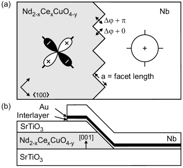
The zigzag-configuration (Fig. 1(a)) has been described in detail in Smildeprl , where it was used to investigate symmetry admixtures in YBa2Cu3O7. In these structures, all interfaces are aligned along one of the -directions of the cuprate, and are designed to have identical -values. With the high- cuprate being an -wave superconductor, the zigzag-structure presents no significant difference to the case of a straight junction aligned along one of the facet’s directions. With the high- superconductor having a -wave symmetry, the facets oriented in one direction experience an additional -phase difference compared to those oriented in the other direction. For a given number of facets, the characteristics of these zigzag structures then depend on the ratio of the facet length and the Josephson penetration depth , see e.g. Zenchuk . In the small facet limit, , the zigzag structure can be envisaged as a one-dimensional array of Josephson contacts with an alternating sign of , leading to anomalous magnetic field dependencies of the critical current, as displayed for YBa2Cu3O7 in Ref. Smildeprl . In the large facet limit, the energetic groundstate includes the spontaneous formation of half-integer magnetic flux quanta at the corners of the zigzag structures, as seen in Hilgenkampnature . All experiments on Nd2-xCexCuO4-y described below are in the small facet limit.
Figure 1(b) schematically shows the Nd2-xCexCuO4-y/Nb ramp-type junctions that were used for the experiments. They were prepared by first depositing a bilayer of 150 nm [001]-oriented Nd2-xCexCuO4-y and 35 nm SrTiO3 by pulsed laser deposition on a [001]-oriented SrTiO3 single-crystal substrate. For the optimally doped films a Nd1.85Ce0.15CuO4 target is used, for the overdoped case a Nd1.835Ce0.165CuO4 target. The Nd2-xCexCuO4-y film is grown at 820 ∘C in 0.25 mbar of oxygen. Subsequently, the temperature is reduced to 740 ∘C for the growth of the SrTiO3 layer in 0.10 mbar of oxygen. Then the deposition chamber is evacuated to about mbar and the sample is kept at 740 ∘C for minutes, before it is slowly cooled down to room-temperature under vacuum conditions. For the Nd1.85Ce0.15CuO4-y films, this procedure yields a typical critical temperature of 20 K, the Nd1.835Ce0.165CuO4-y films had ’s of 13 K. The ’s for Nd1.85Ce0.15CuO4-y and Nd1.835Ce0.165CuO4-y were optimized with respect to the oxygen content. The next step in the junction fabrication process is the etching of a shallow ramp () and cleaning of the sample using argon-ion milling, analogous to the procedure used for YBa2Cu3O7 Smildeprl ; Smildeapl . Then, using the same deposition and cool-down conditions as for the first Nd2-xCexCuO4-y layer, a 12-nm Nd2-xCexCuO4-y interlayer is deposited, followed by the in-situ pulsed-laser deposition of a 12-nm Au barrier layer at 100 ∘C. The interlayer, with the same composition as the base-layer, is employed to provide an in-situ formed interface between the cuprate layer and the Au-barrier. This is found to be of great importance in reaching high junction quality, as it was for the YBa2Cu3O7 case Smildeprl ; Smildeapl . Subsequently, a 160-nm Nb layer forming the counter electrode is deposited by dc-sputtering and structured by lift-off. Finally, the redundant, uncovered Au is removed by ion milling. In addition to zigzag structures with different size and number of facets, every chip contained several straight reference junctions oriented parallel to one of the facet directions.
The junctions were characterized by measuring the current-voltage () characteristics and the dependencies of the critical currents on applied magnetic field , using a four-probe method with the magnetic field parallel to the [001]-direction of the Nd2-xCexCuO4-y in a well-shielded cryostat at K and K. For the determination of , a typical voltage criterion of V was used. This yields a lower limit of to , with being the junctions’ normal state resistance. In the -dependencies presented here, the lowest values can be considered as the lower limit in the determination of the critical current for that respective measurement.
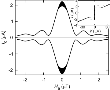
Figure 2 shows the -dependence recorded for a 50 m wide straight Nd1.85Ce0.15CuO4-y/Nb reference junction at K, and in the inset its zero-field -characteristic. The -dependence closely resembles a Fraunhofer pattern, which is the hallmark of small rectangular junctions with homogeneous current distributions. A maximum A at zero applied field was found. The black areas in the peaks of the curves are indicative for the hysteresis in the -characteristics. At the measuring temperature, this junction has a typical of A/cm2, from which a value for the Josephson penetration depth m is estimated. This is several times larger than attainable with grain boundary junctions. The normal-state resistance for this junction is 13 , which gives an product of about 30 V and cm2.
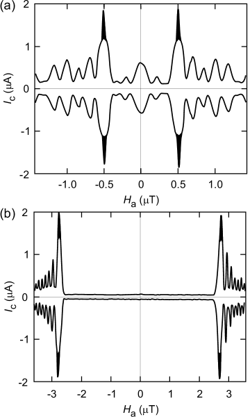
The -dependence for a Nd1.85Ce0.15CuO4/Nb zigzag junction having 8 facets of 25 m width is presented in Fig. 3(a). Instead of an -maximum at , one can observe a maximum of 1.8 A at T. This zigzag junction shows a highly symmetric pattern for both polarities of current bias and applied magnetic field. The critical current at falls to less than 32% of its peak value. Presuming that for this junction is equal to the reference junction described above, the zero field is only 7% of the expected value for an equally long straight junction, disregarding wide-junction effects. It should be noted that also the maximum at T is times lower than expected based on the of the straight junction. Small variations in the thickness of the Au barrier-layer or the Nd1.85Ce0.15CuO4 interlayer between the straight junction and the zigzag structure, placed several mm from each other on the chip, may well account for a considerable part of this -difference. Further, as was shown by Zenchuk and Goldobin Zenchuk , a zigzag structure with an odd number of corners is expected to produce spontaneous magnetic flux for all facet-lengths. As the -dependence of Fig. 3(a) is still strongly non-Fraunhoferlike, this spontaneous flux is expected to be smaller than a half-flux quantum per facet length. Nevertheless, a part of the observed at and the reduced peak height at T may be resulting from this spontaneous flux.
In Fig. 3(b), the -dependence for a zigzag array with 80 facets having a substantially smaller facet length of 5 m is shown, presenting a maximum A at T. Also for this very dense zigzag structure the -dependence is highly symmetric. For this structure, a very low ratio of 2% between the critical current at zero magnetic field and the maximal critical current is found.
The -dependencies of these zigzag structures clearly exhibit the characteristic features also seen for the YBa2Cu3O7 case Smildeprl , namely the absence of a global maximum at and the sharp increase in the critical current at a given applied magnetic field. This behavior can only be explained by the facets being alternatingly biased with or without an additional -phase change. This provides a direct evidence for a -phase shift in the pair wave function for orthogonal directions in momentum space and thus for a predominant order parameter symmetry.
If the order parameter were to comprise an imaginary -wave admixture, the -dependencies for the zigzag junctions would be expected to display distinct asymmetries, especially for low fields Smildeprl . In addition, the critical current at zero applied field is expected to increase with the fraction of -wave admixture. From the high degree of symmetry of the measured characteristics of Figs 3(a) and 3(b) and the very low zero field , no sign of an imaginary -wave symmetry admixture to the predominant symmetry can be distinguished.
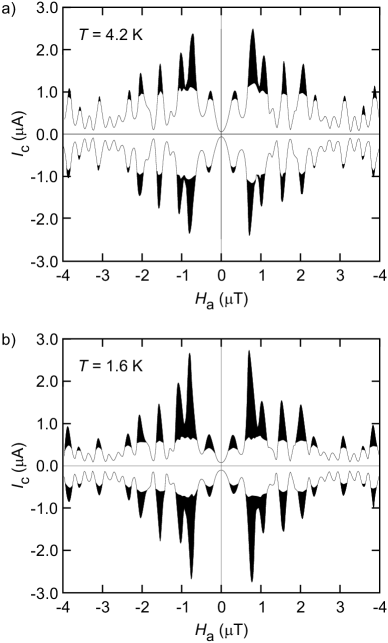
To investigate a possible change of the order parameter symmetry with doping we have fabricated similar zigzag structures using Nd1.835Ce0.165CuO4/Nb junctions. Figure 4(a) shows the -dependence measured at K for a structure with 8 facets of 25 m width. Obviously, also these characteristics indicate a predominant -wave symmetry.
When cooling down the samples to K all the basic features displayed by the structures at K remain unaltered, as is shown for the overdoped sample in Fig. 4(b). We thus see no indication for an order parameter symmetry crossover for Nd1.85Ce0.15CuO4-y in this temperature range, as was recently reported for Pr2-xCexCuO4-y Balci . Similar results were obtained for optimally doped samples upon cooling down to K.
In conclusion, our phase-sensitive order parameter symmetry test experiments based on Nd2-xCexCuO4-y-Nb zigzag junctions provide clear evidence for a predominant order parameter symmetry in the Nd2-xCexCuO4-y. This corroborates the conclusions of studies performed with grain boundary junctions in the optimally doped compounds. To verify various recent reports on possible order parameter changes with overdoping and with decreasing temperature, we have studied the influence of those parameters. No change in the symmetry was observed when overdoping the Nd2-xCexCuO4-y compound. Further, the order parameter symmetry was found to remain unaltered between K and K. This study does not provide an explanation for the contradicting results obtained in other experiments.
Acknowledgements.
The authors thank A. Brinkman, S. Harkema and G. Rijnders for helpful discussions. This work was supported by the Dutch Foundation for Research on Matter (FOM), the Netherlands Organization for Scientific Research (NWO) and the European Science Foundation (ESF) PiShift programme.References
- (1) D. J. Van Harlingen, Rev. Mod. Phys. 67, 515 (1995).
- (2) C. C. Tsuei and J. R. Kirtley, Rev. Mod. Phys. 72, 969 (2000).
- (3) C. C. Tsuei and J. R. Kirtley, Phys. Rev. Lett. 85, 182 (2000).
- (4) B. Chesca et al., Phys. Rev. Lett. 90, 057004 (2003).
- (5) J. W. Ekin et al., Phys. Rev. B 56, 13746 (1997).
- (6) S. Kashiwaya et al., Phys. Rev. B 57, 8680 (1998).
- (7) L. Alff et al., Phys. Rev. B 58, 11197 (1998).
- (8) J. A. Skinta et al., Phys. Rev. Lett. 88, 207005 (2002).
- (9) M. -S. Kim et al., Phys. Rev. Lett. 91, 087001 (2003).
- (10) L. Alff et al., Phys. Rev. Lett. 83, 2644 (1999).
- (11) S. M. Anlage et al., Phys. Rev. B 50, 523 (1994).
- (12) D. H. Wu et al., Phys. Rev. Lett. 70, 85 (1993).
- (13) A. Andreone et al., Phys. Rev. B 49, 6392 (1994).
- (14) N. P. Armitage et al., Phys. Rev. Lett. 86, 1126 (2001).
- (15) T. Sato et al., Science 291, 1517 (2001).
- (16) J. D. Kokales et al., Phys. Rev. Lett. 85, 3696 (2000).
- (17) R. Prozorov et al., Phys. Rev. Lett. 85, 3700 (2000).
- (18) F. Hayashi et al., J. Phys. Soc. Jpn. 67, 3234 (1998).
- (19) B. Chesca et al., Condmat-0402131(2003).
- (20) A. Biswas et al., Phys. Rev. Lett. 88, 207004 (2002).
- (21) M. M. Qazilbash et al., Phys. Rev. B 68, 024502 (2003).
- (22) H. Balci and R. L. Greene, Cond-mat 0402263 (2004).
- (23) H. J. H. Smilde et al., Phys. Rev. Lett. 88, 057004 (2002).
- (24) A. Zenchuk and E. Goldobin, Phys. Rev. B 69, 024515 (2004).
- (25) H. Hilgenkamp et al., Nature 422, 50 (2003).
- (26) H. J. H. Smilde et al., Appl. Phys. Lett. 76, 912 (2002).