Huge excitonic effects in layered hexagonal boron nitride
Abstract
The calculated quasiparticle band structure of bulk hexagonal boron nitride using the all-electron GW approximation shows that this compound is an indirect-band-gap semiconductor. The solution of the Bethe-Salpeter equation for the electron-hole two-particle Green function has been used to compute its optical spectra and the results are found in excellent agreement with available experimental data. A detailed analysis is made for the excitonic structures within the band gap and found that the excitons belong to the Frenkel class and are tightly confined within the layers. The calculated exciton binding energy is much larger than that obtained by Watanabe et alwatanabe_taniguchi using a Wannier model to interpret their experimental results and assuming that h-BN is a direct-band-gap semiconductor.
pacs:
71.15.Mb, 71.35.Cc, 78.20.-eHexagonal boron nitride (h-BN) is one of the most anisotropic layer compounds and represents an interesting quasi-two-dimensional insulator analog to semi-metallic graphite. Due to its high thermal stability, h-BN is a widely used material in vacuum technology. It has been employed for microelectronic devicespauli , for x-ray lithography masksdana , and as a wear-resistant lubricantmiyoshi . The interest in h-BN has been renewed by the possibility of preparing boron nitride nanotubes that are far more resistant to oxidation than carbon nanotubes and therefore suited to high temperature applications. As their band gaps are predicted to be weakly dependent on helicity and tube diameterrubio_corkill ; blase_rubio , unlike tubes made of carbon, it has the potential of revolutionizing the electronics industry. To understand the quasiparticle properties of BN nanotubes one has first to have a complete understanding of the electronic and optical properties of bulk h-BN since BN nanotubes can be viewed as a rolled up BN sheets.
Despite the large number of experimentstegeler ; zunger_katzir ; hoffman ; mamy ; watanabe_taniguchi devoted to the study of the electronic properties of bulk h-BN, both the direct and the indirect band-gap are not yet accurately known, i.e., values ranging from 3.2 to 5.97 eV have been reported in the literature. In particular, the latest results were obtained by Watanabe et alwatanabe_taniguchi , who showed that this material is very promising for ultraviolet laser devices and assumed, based on the strong luminescence peak observed at 5.765 eV, that it is a direct-band-gap semiconductor. In addition, they inferred a gap of 5.971 eV in contradiction with our results and other GW quasiparticle calculationsblase ; capellini_satta ; capellini_fiorentini .
In this Letter, we use our all-electron GW approximationbrice to study for the first time the optical properties of bulk h-BN including electron-hole interaction effects and show that the previous experimental interpretation of the excitonic structure in the band gap is not correct. To perform this study we used state of the art methods, where both the self-energy effects and the solution of the Bethe-Salpeter equationonida_reining to compute the optical spectra from first principlesarnaud_2001 . In particular, our study confirms that this material is an indirect-band-gap semiconductor in agreement with previous GW calculationblase ; capellini_satta ; capellini_fiorentini , and that the interpretation of the optical spectra of h-BN, upon which the band gap of Watanabe et alwatanabe_taniguchi is based, is very intricate as they are dominated by strong electron-hole interaction effects. We show that theoretical optical spectra are reliable and are in excellent agreement with experimentmamy . In addition, we show that the exciton in the band gap belongs to a Frenkel class instead of a Wannier class as proposed by Watanabe et alwatanabe_taniguchi from the analysis of their experimental data, and we found that its binding energy is huge compared to theirs.
The crystalline structure of h-BN is hexagonal and has the D group symmetry. It consists of hexagonal graphite-like sheets but with an ABAB stacking with boron atoms in layer A found directly below nitrogen atoms in layer B. The ground state properties of h-BN are obtained by means of the all-electron Projector-Augmented-Wave method (PAW)Bloechl from density-functional theory (DFT) in the local-density approximation (LDA)perdew , yielding LDA band-structure energies, and wave functions needed to calculate all quantities occurring in the GW self-energy operator and the electron-hole interaction. The experimental lattice parameterssolozhenko (a=4.73 a.u and c/a=2.66) are used to perform all calculations.
The quasiparticle energies are determined by solving the QP equation, where the self-energy operator is written down in Hedin’s GW approximation hedin which includes dynamic polarization in the random-phase approximation (RPA). In this case can be written as the product of the Green’s function and the dynamically screened Coulomb interaction within the RPA. In this work, a plasmon pole modelhorsch is used to mimic the frequency dependence of the dielectric matrix in order to reduce the computational cost of the GW calculations. More details about our implementation are given elsewherebrice .

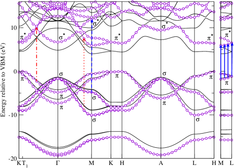
In Fig. 1, both the calculated LDA (thin solid lines) and GW (solid lines with open circles) band structures are plotted along the high symmetry directions. Within the LDA, we found an indirect gap of 4.02 eV between the bottom of the conduction band at the point and the top of the valence band near ( point). The minimum direct gap is located at the point and is 4.46 eV. Our results are in excellent agreement with other LDA calculations blase ; xu_ching ; furthmuller . The main effect of the self-energy correction is to increase the gap from 4.02 eV (LDA) to 5.95 eV and the minimum direct gap from 4.46 eV (LDA) to 6.47 eV. Our GW results are in good agreement with the calculations of Capellini et alcapellini_fiorentini who found values 6.04 and 6.66 eV, respectively. Figure 1 shows also that the GW corrections to the LDA are strongly dependent on the degree of orbital localization and that the overall corrections can not be reproduced by a rigid band shift of the conduction states with respect to the top of the valence states. Such a behavior has already been reported for layered compounds like graphitestrocov or LiBC lebegue_libc .
The wide range of experimental valuestegeler ; zunger_katzir ; hoffman ; mamy ; watanabe_taniguchi reported for the band gap (between 3.2 and 5.97 eV) may be due, in large part, to the difficulty to synthesize high quality h-BN crystals or to the difficulty to extract the band gaps from experiment. The most accurate results have been obtained by Watanabe et al.watanabe_taniguchi who resolved the excitonic structure within the gap at very low temperature (8 K) and deduced from the identification of a plateau in their absorption spectrum that the QP gap is 5.971 eV. Notice that the inferred band gap is very close to our calculated indirect band gap. It’s worth pointing out that the interpretation of the optical spectra of non-conducting solids is very intricate because of strong electron-hole correlation effects.
In the absence of exciton-phonon coupling, emission or absorption of a photon involves excited states of total wavevector corresponding to the photon momentum, hereafter approximated as . Due to electron-electron interaction, these excited states can be viewed as a linear combination of quasielectron-quasihole pairs:
| (1) |
where creates a quasielectron and a quasihole in the many-body ground state . The electron-hole amplitudes and the excitation energies are obtained by solving an effective two-particle Schrödinger equation, which originates from the Bethe-Salpeter equationstrinati and provides the key ingredients to calculate the imaginary part of the dielectric function including both local field (LF) and excitonic effectsarnaud_2001 ; arnaud_2005 .
As the screening controls the strength of the electron-hole interaction, we inverted directly the dielectric function at the RPA level to obtain the static dielectric function . The LDA, without LF effects, produces values of 4.67 and 2.98 for and , respectively, where is the electric field vector. As expected, the LF effects push the oscillator strength towards higher energiesmarinopoulos reducing the static dielectric function values to 4.40 and 2.53, respectively. Notice that the LF have a stronger effect for the out of plane polarization, i.e., . This is due to the rather large inhomogeneity of the h-BN charge density along the direction. These results show that the screening is rather anisotropic and that excitonic effects are expected to be important, i.e., the smaller dielectric constant, the larger the excitonic effects due to the poor screening of the electron-hole interaction.

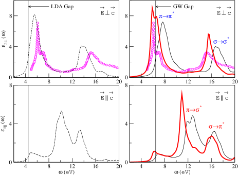
The calculated optical absorption spectra for h-BN with and without excitonic effects are shown in Fig. 2 and are compared to the experimental resultsmamy for in-plane polarization (). The LDA-RPA (dashed line) and the GW-RPA (thin solid line) dielectric functions are red-shifted and blue-shifted with respect to experiment, respectively. Notice that the GW-RPA spectra can not be obtained by simply shifting the LDA-RPA spectra towards higher energies because the corrections to the LDA eigenvalues are far from being uniform across the BZ. The GW-RPA spectrum for the in-plane polarization exhibits two prominent structures located at 7.65 eV and 16.65 eV, respectively. The first structure originates from the interband transitions between two parallel bands along the M-L high symmetry direction and is denoted by solid arrows in Fig. 1. For such transitions, the charge densities for the valence and the conduction states both have a character and are located on nitrogen and boron atoms, respectively. The second peak originates from interband transitions. One of the corresponding interband transition, occurring at the M point, is depicted by a dashed arrow on Fig. 1. The GW-RPA spectrum for out-of-plane polarization () displays three major structures located at 12 eV, 12.75 eV and 16.5 eV and originate from or interband transitions. The dot-dashed and dotted arrows on Fig. 1 represent one of the interband transitions contributing to the peaks located at 12.75 eV and 16.5 eV, respectively.
The assignment of the optical transitions for both polarization directions can be understood by invoking symmetry arguments. Since there is a mirror plane within each layer, it’s possible to separate bands into states of even () and odd () parity. Therefore, only transitions between bands of the same symmetry ( and ) are allowed for in-plane polarization (), while only transitions between bands of different parity ( and ) are allowed for out-of-plane polarization. Notice that this selection rule is only valid for points whose component along the axis is strictly zero. Thereby, we can explain the rather small but non vanishing oscillator strength below 10 eV for the out-of-plane polarization.

Figure 2 also shows the calculated spectra including excitonic effects (thick solid line). The electron-hole attraction shifts the oscillator strength towards lower photon energies by about 1 eV, bringing the calculated spectra in better agreement with experiment. A bound exciton shows up at 5.85 eV in the calculated spectra while a prominent peak occurs at 6.08 eV in the experimental spectrum. It is interesting to point out that a peak around 6.15 eV, characteristic of h-BN, has been found in the absorption spectrum of single-wall boron nitride nanotubeslauret . A detailed analysis of our calculated peak shows that it’s made of four excitonic lines located at 5.75 , 5.78 , 5.82 and 5.85 eV. Each of this excitonic state is built from a coherent superposition of quasielectron-quasihole pairs corresponding to transitions between the two last valence bands and the two first conduction bands for points laying in the HLMK plane. The points which contribute the most to these excitonic lines are distributed along directions parallel to the axis and in the direction HK, where the bands are nearly parallel (see Fig. 1). Notice that these excitonic peaks are only visible for in-plane polarization because bands of the same parity () are involved in these excited states. Again, it’s worth comparing our results with those of Watanabe et al.watanabe_taniguchi who found four excitonic lines located at 5.822, 5.945, 5.962 and 5.968 eV, respectively. These lines were attributed to a series of s-like excitons () by using a Wannier model and estimating the band gap to be 5.971 eV. The overall agreement with our results is pretty good when we shift our calculated excitonic lines by 0.07 eV towards higher energy. Nevertheless, we do not reproduce the experimental spacing between the different lines. Such a difference might be due to the approximations made to solve the Bethe-Salpeter equation. Regarding the interpretation of the excitonic structures inside the gap, our results strongly disagree with those of Watanabe et al who inferred a binding energy of 0.149 eV from their optical absorption spectra. Indeed, our results show that the binding energy is much larger, 0.72 eV, and that excitons in h-BN belong to the Frenkel and not to the Wannier class.
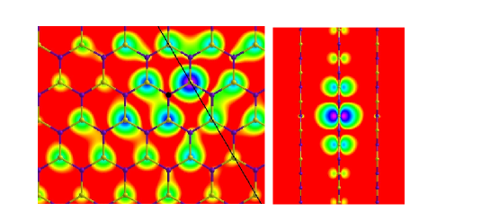
To address the localization of the excitons for h-BN, we calculate the exciton probability for a given hole position and show the distribution of the electron relative to the hole for the excited state at 5.78 eV. Figure 3 displays such a distribution for a hole localized slightly above a nitrogen atom. The left panel shows that the electron is delocalized on boron atoms and that the probability of finding the electron on a boron atom is maximum for the nearest neighbors of the nitrogen atom where the hole is localized. The right panel shows that the electron is confined within the layer where the hole is located, which is expected because the screening is rather poor along the direction. The distribution of the electron relative to the hole also reflects the orbital character of the conduction states which have a pz character on B atoms. Similar plots have been obtained for other bound excitons, confirming that the Frenkel exciton-like picture is valid.
In this letter, results concerning the excited states of h-BN have been presented. By calculating the quasiparticle band structure within the GW approximation, we found that h-BN is an indirect gap semiconductor with a band gap energy of 5.95 eV in surprisingly close agreement with the supposed direct gap of 5.971 eV reported by Watanabe et alwatanabe_taniguchi while our calculated minimum direct band gap is 6.47 eV. We solved the Bethe-Salpeter equation to calculate the optical spectra and obtained a good agreement with the experimental results of Ref.mamy for in-plane polarization up to 20 eV. A detailed analysis of the four excitonic structures within the gap shows that these structures are related to transitions across the gap. In addition, we deduced a binding energy of 0.72 eV in strong disagreement with the value of 0.149 eV found in Ref. watanabe_taniguchi . On the one hand, the large excitonic binding energy ( kT) explains the unusual strong luminescence peak for an indirect semiconductor observed by Watanabe et al at 5.765 eV, and on the other hand it explains why this peak does not show noticeable temperature dependence. Finally, we believe that this work is a first step towards a better understanding of large excitonic effects reported for single-wall boron nitride nanotubeslauret .
Supercomputer time was provided by the CINES (project gmg2309) on the IBM SP4. We would like to acknowledge partial support from the GDR-DFT.
References
- (1) K. Watanabe, T. Taniguchi, and H. Kanda, Nature Materials 3, 404 (2004).
- (2) T.K. Pauli, P. Bhattacharya, and D.N. Bose, Appl. Phys. Lett. 56, 2648 (1990).
- (3) S.S. Dana, Mater. Sci. Forum 54-55, 229 (1990).
- (4) K. Miyoshi et al., Surf. Coat. Technol. 33, 221 (1987).
- (5) A. Rubio, J.L. Corkill, and M. L. Cohen, Phys. Rev. B 49, R5081 (1994).
- (6) X. Blase, A. Rubio, S.G. Louie, and M. L. Cohen, Europhys. Lett. 28, 335 (1994).
- (7) E. Tegeler et al., Phys. Status Solidi B 91, 223 (1979).
- (8) A. Zunger, A. Katzir, and A. Halperin, Phys. Rev. B 13, 5560 (1976).
- (9) D.M. Hoffman, G.L. Doll, and P.C. Eklund, Phys. Rev. B 30, 6051 (1984).
- (10) R. Mamy, J. Thomas, G. Jezequel, and J.C. Lemonnier, J. Phys. (Paris) Lett. 42, 473 (1981).
- (11) X. Blase, A. Rubio, S.G. Louie and M. L. Cohen , Phys. Rev. B 51, 6868 (1995).
- (12) G. Cappellini, G. Satta, M. Palummo and G. Onida, Phys. Rev. B 64, 035104 (2001).
- (13) G. Cappellini, V. Fiorentini, K. Tenelsen, and F. Bechstedt, Gallium Nitride and Related Materials, Edited by R.D. Dupuis, J.A. Edmond, F.A. Ponce, and S. Nakamura, (Mater. Res. Soc. Symp. Proc. No 395, Materials Research Society, Pittsburgh, 1996)
- (14) B. Arnaud and M. Alouani, Phys. Rev. B 62, 4464 (2000).
- (15) G. Onida, L. Reining, and A. Rubio, Rev. Mod. Phys. 74, 601 (2002).
- (16) B. Arnaud and M. Alouani, Phys. Rev. B 63, 85208 (2001).
- (17) P.E Blöchl, Phys. Rev. B 50, 17953 (1994).
- (18) J. P. Perdew and A. Zunger, Phys. Rev. B 23, 5048 (1981).
- (19) V.L. Solozhenko, G. Will and F. Elf, Solid State Commun. 96, 1 (1995).
- (20) L. Hedin, Phys. Rev. 139, A796, (1965).
- (21) W. von der Linden and P. Horsch, Phys. Rev. B 37, 8351 (1988).
- (22) J. Furthmüller, J. Hafner, and G. Kresse, Phys. Rev. B 50, 15606 (1994).
- (23) Y.N. Xu and W.Y. Ching, Phys. Rev. B 44, 7787 (1991).
- (24) V. N. Strocov et al., Phys. Rev. B 64, 75105 (2001).
- (25) S. Lebègue, B. Arnaud, P. Rabiller, M. Alouani, and W. E. Pickett, Europhys. Lett. 68, 846 (2004).
- (26) G. Strinati, Phys. Rev. B 29, 5718 (1984).
- (27) B. Arnaud, S. Lebègue and M. Alouani, Phys. Rev. B 71, 035308 (2005).
- (28) A. G. Marinopoulos, L. Reining, A. Rubio, and V. Olevano, Phys. Rev. B 69, 245419 (2004).
- (29) J. S. Lauret et al., Phys. Rev. Lett. 94, 037405 (2005).