Strain Relief in Cu-Pd Heteroepitaxy
Abstract
We present experimental and theoretical studies of Pd/Cu(100) and Cu/Pd(100) heterostructures in order to explore their structure and misfit strain relaxation. Ultrathin Pd and Cu films are grown by pulsed laser deposition at room temperature. For Pd/Cu, compressive strain is released by networks of misfit dislocations running in the [100] and [010] directions, which appear after a few monolayers already. In striking contrast, for Cu/Pd the tensile overlayer remains coherent up to about 9 ML, after which multilayer growth occurs. The strong asymmetry between tensile and compressive cases is in contradiction with continuum elasticity theory, and is also evident in the structural parameters of the strained films. Molecular Dynamics calculations based on classical many-body potentials confirm the pronounced tensile-compressive asymmetry and are in good agreement with the experimental data.
pacs:
68.55.-a, 68.35.Gy, 81.15.FgHeteroepitaxy with different thicknesses ranging from monoatomic layers up to micrometers produces various structures, and is one of most important routes to artificially obtain functional materials and devices. Stress and its relaxation due to an interface lattice mismatch are an essential problem in the heterostructures. Classical continuum theory defines the concept of an equilibrium critical thickness , above which the lattice stress relaxes with the introduction of a misfit dislocation (MD) CCM . The critical thickness is determined by energy balance between strain energy buildup and strain relief due to dislocation nucleation in the mismatched structure. The value of predicted by the continuum theory, however, often does not agree with experiments. Moreover, the critical thickness in the continuum elasticity theory is independent on the strain type, be it tensile or compressive. Atomic details of the interface structure such as surface steps and surface roughness, are usually ignored. Actual stress relaxation of coherent strained films is kinetically limited, typically with high barriers. Recently, atomistic studies on model systems have been done to determine the transition paths and energy barriers from coherent to incoherent states in real epitaxial films Dong:98 ; Trushin:02 ; Trushin:03 . One of the main findings has been a striking asymmetry between the tensile and compressive cases, due to the anharmonicity and asymmetry of the atomic interactions Trushin:02 ; Trushin:03 . Further, the concept of a size-dependent mesoscopic mismatch has been proposed to explain strain relaxations in the early stage of homo and heteroepitaxial metal growth on the atomic scales Kirschner .
In this Letter, we present results from a combined experimental and theoretical study on a model system of Cu-Pd heteroepitaxy grown by pulsed laser deposition (PLD). The bulk lattice parameters of Cu and Pd are Å and Å, respectively. The lattice misfit induces a large compressive () strain in the Pd overlayer on Cu(100) and a tensile () strain for the Cu overlayer on Pd(100). The Pd films on Cu(100) and the Cu films on Pd(100) were grown by pulsed laser deposition (PLD) in a multi-chamber ultrahigh vacuum (UHV) system with a base pressure mbar, and mbar during deposition. Prior to deposition the copper and palladium substrates were cleaned by cycles of Ar+ sputtering followed by annealing at K for Cu substrate or K for Pd substrate until clean Auger electron spectroscopy (AES) spectra, sharp low-energy electron diffraction (LEED) spots, and atomically smooth terraces under scanning tunneling microscopy (STM) were observed. The substrate temperature was kept at room temperature during deposition. The substrate was placed about mm away from targets. A KrF excimer laser beam (wavelength nm, pulse duration ns, typical pulse energy mJ and pulse repetition rate of Hz) was focused onto targets. During deposition the growth process was monitored by a reflection high energy electron diffraction (RHEED). All STM measurements were performed in the constant current mode at a V positive tip bias and a nA tunneling current. Compared to thermal deposition (TD), an extremely high instantaneous flux of atoms in PLD favors much larger nucleation density Jenniches1:99 ; Ohresser:99 . This helps to suppress the formation of Cu(001)-Pd ordered alloy in the initial growth stage for Pd/Cu(100) Murray:95 and the phase transition at 1 ML from fcc to bct structure for Cu/Pd(100) Hahn:95 . Even though the present STM setup does not provide a direct distinction of the Pd and Cu atoms, neither pits in the substrate surface nor eroded substrate step edges show any evidence of Cu-Pd interlayer mixing. Moreover, the surface area covered by the islands for submonolayer coverages, as determined from STM images, are always consistent with the coverage from RHEED. The RHEED data confirm the layer-by-layer growth mode for both systems. It persists up to at least ML in Cu-Pd heteroepitaxy.
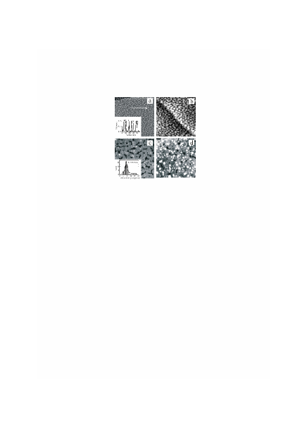
Figures 1(a)-(d) display STM images taken at room temperature for Pd films on Cu(100). For submonolayer Pd at ML, many islands with a monolayer height of about Å were observed as shown in the inset of Fig. 1(a). With increasing Pd thickness such islands are always formed on a completely filled underlayer up to a total thickness of about ML, indicating ideal 2D growth mode. Above ML a striking feature is the appearance of misfit dislocations as marked by many protruding stripes with an average height of Å (see Fig. 1(c) and (d)), by which the compressive stress in Pd film relaxes efficiently. They align nearly regularly along the [100] and [010] directions. The average spacing of MD lines is nm for ML. The layer-by-layer growth persists up to ML, after which multilayer growth mode occurs.
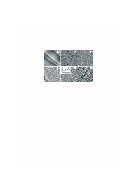
The corresponding layer-by-layer growth mode for PLD Cu films on Pd(100) has also been confirmed by STM images as indicated in Fig. 2. At ML, second layer nucleation is not found, while in the ML thick film more than % of the second layer is accomplished (Figs. 2(b) and (c)). At ML, few of the islands in the third layer have a preferential orientation, whereas at ML most of the fourth layer islands are rectangular along the directions. With increasing Cu thickness to ML, % of the sixth layer is completed, where nearly all the pits in the sixth layer and the seventh layer islands are rectangular. Above ML the morphology of Cu films is changed because of the multilayer growth mechanism. A typical image for ML is given in Fig. 2(f). Four layers appear simultaneously on the surface. Moreover, only % of the ninth layer is completed while the remaining % appears as the tenth and eleventh layers. It should be pointed out that the height or depth of all (ir)regular islands and pits is about Å until ML as shown in the inset of Fig. 2(d). This vertical magnitude corresponds to the interlayer spacing of highly strained fcc Cu Li:91 . In PLD Cu films on Pd(100) we have not found any trace of dislocation nucleation up to ML. Above ML, the multilayer island structure with the orientation is still visible and the film surface becomes more and more rough.
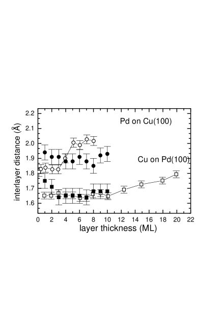
IV-LEED measurements of the specularly scattered electron beam were done to obtain structural information on the films. The average interlayer spacing of PLD films was calculated from LEED intensity of the (00) diffraction beam vs. energy curves based on a kinetic model Zharnikov:96 . Fig. 3 gives the layer thickness dependence of the interlayer distance for both systems. In the case of Pd/Cu(100) films, the interlayer distance is about Å up to ML, very close to the value of Cu substrate, and increases rapidly above ML to reach the value of bulk Pd. For Cu on Pd(100) up to ML, the value stays constant ( Å). This agrees well with the measured height of monolayer islands by STM. Above ML the interlayer spacing gradually increases close to the value of bulk fcc Cu at a coverage of ML.
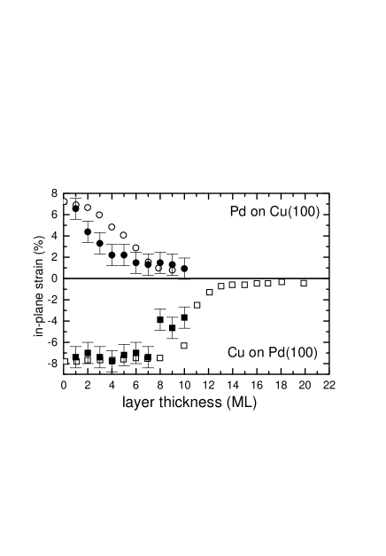
The actual in-plane lattice constant of deposited films was obtained in situ by measuring the spacing between the reciprocal lattice rods in the RHEED image. The RHEED spacing of substrates serves as a reference. The in-plane lattice strain is defined as (%). Fig. 4 gives the measured data. For Pd/Cu(100), the measured in-plane strain exhibits a gradual decrease with increasing thickness of the Pd film. The compressive strain is nearly fully relaxed at ML. In contrast, the in-plane tensile strain shows a very different thickness dependence in the case of PLD Cu films on Pd(100). Until ML only % reduction in the tensile strain is found. Above ML a step-like decrease is visible and a residual strain is observed until ML.
The most striking discovery in our data is the strong asymmetry in the strain relaxation behavior between the tensile and compressive strained films. This result is in direct disagreement with the continuum elasticity theory, which predicts a symmetrical behavior for tensile and compressive systems.
In any growth mode, there is always the question whether the final configuration is dictated by kinetic considerations or it corresponds to a true thermodynamic equilibrium state. Given the lack of precise characterization of the PLD growth conditions, a full theoretical modeling of the kinetic growth process under the experimental conditions is unfeasible. Instead, we have chosen to perform equilibrium molecular dynamics simulations of the epitaxial layer after deposition. The object here is to study the thermal excitation and nature of dislocations in the epitaxial film and to see whether they can account for the observed stress relaxation and tensile compressive asymmetry in Cu-Pd heterostructures. Our atomistic model contains five layers of substrate and varying number of film layers. Two bottom layers of the substrate were fixed. Periodic boundary conditions were applied in the plane parallel to the surface. The lateral size of the systems studied varied between to . Interatomic forces between particles in the system were computed using Embedded Atom Model (EAM) potentials for Cu and Pd eam . The initial configuration of the film has adatoms occupying fcc positions in registry with substrate.
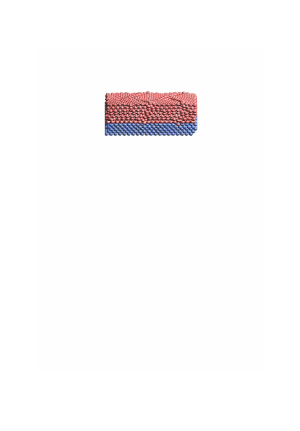
For Pd/Cu(100), after thermal equilibrium is reached at K, the system relaxes and gains partial strain relief through generation of misfit dislocations starting at ML and above. To facilitate a direct comparison with the experimental data in Fig. 3, we computed from our simulations the average interlayer distance for the top layers of the film (up to three to take into account the surface sensitivity of LEED). We also computed the average in-plane lattice constant for the top three surface layers, and then evaluated the in-plane strain using the bulk value of the adsorbate as a reference. The dependence of these values on the film thickness is shown in Fig. 4. There is a good qualitative agreement between the theoretical results with the experimental observation showing continuous relief of in-plane strain through the misfit dislocations. The exact nature of the misfit dislocations is rather complicated, varying both as a function of film thickness and lateral size. In Fig. 5, we show a typical configuration for a film of ML thickness and lateral size obtained by molecular dynamics annealing through heating to K, followed by cooling to K. This shows a Pd film with misfit dislocations visibly aligned along the direction of the substrate, in agreement with the experimental observations.
Simulation studies were also performed for Cu/Pd(100). Here, in agreement with the experimental observation, the theory shows a striking difference from the Pd/Cu(100) system. The pseudomorphic strained fct structure for the Cu film remains stable up to about ML. Then strain is gradually released through localized surface defect such as vacancies and adatoms, rather than the misfit dislocation mechanism observed in Pd/Cu(100). The theoretical results for the average interlayer distance of the film and the in-plane strain for the top surface layers as a function of the film thickness are shown in Figs. 3 and 4, respectively. The theory again is in good agreement with the experimental data, indicating a stable highly strained epitaxial state below ML.
In conclusion, we have studied the stress relaxation mechanism in Cu-Pd heteroepitaxy both through PLD experiments and numerical simulations. The experimental data show that for Pd/Cu(100), the in-plane stress is relaxed almost immediately above ML, whereas Cu/Pd(100) remains coherent up to about ML. While these observations contradict predictions from the continuum theory, they are confirmed by our atomistic simulations using EAM potentials for the Pd and Cu interactions. The good agreement between the experimental data and the equilibrium simulation study leads us to conclude that the observed configurations of the film at different thicknesses correspond to equilibrium state with thermally generated misfit dislocations as the strain relief mechanism. The microscopic nature of the misfit dislocation observed here for the Pd/Cu(100) system is rather complicated and does not fit into the simple model postulated previously muller .
On a microscopic level, the tensile-compressive asymmetry originates from the asymmetry of the interatomic interactions. The general feature of interatomic potentials is a steeply rising repulsive part at small separations as opposed to a very slowly decreasing attractive part at large separations. This strong asymmetric feature of the interaction is what leads to the observed macroscopic tensile-compressive asymmetry. We have performed additional studies using very different potentials (of Lennard-Jones type) with the same general feature, and the results indeed remain qualitatively unchanged. Interestingly, we find that geometry and dimension play an important role in the tensile-compressive strain relief asymmetry. For the 2D model, misfit dislocations are favored for tensile rather than compressive strained systems Trushin:02 ; Trushin:03 . Clearly, there is much more to learn in strain relief in heteroepitaxy through further theoretical and experimental investigations.
Y. Lu acknowledges support from the MPI in Halle during his stay there. This work has been supported in part by Fundação de Amparo à Pesquisa do Estado de São Paulo - FAPESP (grant no. 03/00541-0) (E.G.), the Academy of Finland through its Center of Excellence program (T.A-N. and O.T.), and CRDF grant RU-P1-2600-YA-04 (O.T.).
References
- (1) J. W. Matthews, J. Vac. Sci. Technol., 12, 126 (1975).
- (2) Liang Dong, Jurgen Schnitker, Richard W. Smith, and David J. Srolovitz, J. Appl. Phys. 83, 217 (1998).
- (3) O. Trushin, E. Granato, S. C. Ying, P. Salo, and T. Ala-Nissila, Phys. Rev. B 65, 241408 (2002).
- (4) O. Trushin, E. Granato, S. C. Ying, P. Salo, and T. Ala-Nissila, Phys. Rev. B 68, 155413 (2003).
- (5) V. S. Stepanyuk, D. I. Bazhanov, W. Hergert, and J. Kirschner, Phys. Rev. B 63, 153406 (2001); O. V. Lysenko, V. S. Stepanyuk, W. Hergert, and J. Kirschner, Phys. Rev. Lett. 89, 126102 (2002); V. S. Stepanyuk, D. V. Tsivlin, D. Sander, W. Hergert, and J. Kirschner, Thin Solid Films 428, 1 (2003).
- (6) H. Jenniches, J. Shen, Ch. V. Mohan, S. Sundar Manoharan, J. Barthel, P. Ohresser, M. Klaua, J. Kirschner, Phys. Rev. B 59, 1196 (1999).
- (7) P. Ohresser, J. Shen, J. Barthel, M. Zheng, Ch. V. Mohan, M. Klaua, and J. Kirschner, Phys. Rev. B 59, 3696 (1999).
- (8) P. W. Murray, I. Stensgaard, E. Læsgaard, and F. Besenbacher, Phys. Rev. B 52, R14404 (1995); A. Bilic, Y.G.Shen, B.V. King, and D.J. O’Connor, Surf. Rev. Lett. 5, 959 (1998); J. Kudrnovsky, S.K Bose, and V. Drchal, Phys. Rev. Let. 69, 308 (1992).
- (9) E. Hahn, E. Kampshoff, N. Wälchli, and K. Kern, Phys. Rev. Lett. 74, 1803 (1995); I.A. Morrison, M.H. Kang, and E.J. Mele, Phys. Rev. B 39, 1575 (1989); T. Kraft, P.M. Marcus, M. Methfessel, and M. Scheffer, Phys. Rev. B 48, 5886 (1993).
- (10) Y. S. Li, J. Quinn, H. Li, D. Tian,and F. Jona, Phys. Rev. B 44, 8261 (1991).
- (11) M. Zharnikov, A. Dittschar, W. Kuch, C. M. Schneider, J. Kirschner, Phys. Rev. Lett. 76, 4620 (1996).
- (12) S. M. Foiles, M. I. Bakes, and M. S. Daw, Phys. Rev. B 33, 798 (1986).
- (13) B. Müller, B. Fischer, L. Nedelmann, A. Fricke, and K. Kern, Phys. Rev. Lett. 76, 2358 (1996).