Distinct Pairing Symmetries in and Single Crystals: Evidence from Comparative Tunnelling Measurements
Abstract
We used point-contact tunnelling spectroscopy to study the superconducting pairing symmetry of electron-doped (NCCO) and hole-doped (LSCO). Nearly identical spectra without zero bias conductance peak (ZBCP) were obtained on the (110) and (100) oriented surfaces (the so-called nodal and anti-nodal directions) of NCCO. In contrast, LSCO showed a remarkable ZBCP in the nodal direction as expected from a -wave superconductor. Detailed analysis reveals an -wave component in the pairing symmetry of the NCCO sample with , a value remarkable close to that of a weakly coupled BCS superconductor. We argue that this s-wave component is formed at the Fermi surface pockets centered at (,0) and (0,) although a -wave component may also exist.
pacs:
74.50.+r, 74.72.Jt,74.45.+cI Introduction
For hole-doped cuprate superconductors, there is a well-known electronic phase diagram characterized by a dome-like superconducting region when is above a certain threshold OrensteinJ2000 . It was found that TokuraY1989 instead of doping holes into the Cu-O plane, one can also achieve superconductivity by doping electrons into the Cu-O plane in systems like Ln2-xCexCuO4 with Ln = Nd, Pr, La, etc. One thus naturally questions whether the superconducting mechanism is the same between the hole- and electron- doped cuprates. Among many superconducting properties, the symmetry of the order parameter is an important one. While the symmetry of the superconducting order parameter is believed to be -wave for the hole-doped region TsueiCC2000 , the situation for electron-doped materials is highly controversial. For example, Angle-resolved photoemission spectroscopy (ARPES) ArmitageNP2001 , specific heat BalciH2002 , phase-sensitive scanning SQUID TsueiCC2000PRL , bi-crystal grain-boundary Josephson junctionChesca and some penetration depth measurements Penetrationdepth01 ; SnezhkoA2004 indicate a -wave symmetry. In addition, Raman scattering BlumbergG2002 and recent ARPES MatsuiH2004 experiments show a nonmonotonic -wave order parameter. However, this has been contrasted by tunnelling ChenCT2002 ; KashiwayaS1998 and some other specific heat LiuZY2004 and penetration depth measurements AlffL1999 ; SkintaJA2002 ; KimMS2003 . In particular, there may be a crossover from -wave to -wave symmetries by changing the doped electron concentration SkintaJA2002b ; BiswasA2002 or decreasing temperature BalciH2004 . Although such a crossover may explain the conflicting experimental results on the pairing symmetry in the electron-doped cuprates, the characteristics of such possible -wave pairing symmetry has yet to be established.
In this paper, we report directional tunnelling measurements on single crystals of optimally electron-doped cuprate (NCCO). By injecting current along either the Cu-Cu bond (110) or Cu-O bond (100) direction, we obtain nearly identical tunnelling spectra indicating an -wave component of the pairing symmetry in this material. For comparison, similar measurements were carried out on underdoped -type single crystals of (LSCO), and we observe clear zero bias conductance peaks (ZBCP) in tunneling spectra along the (110) direction as expected from the -wave symmetry. Our results thus indicate that the optimally doped NCCO has at least an unavoidable -wave component, which is in contrast with the case in hole-doped LSCO where a pure -wave has been established.
II Experimental details
We grew the NCCO and LSCO single crystals using the travelling-solvent floating-zone technique OnoseY2001 ; ZhouF2003 . As shown in Fig. 1, the resistive curve measured on the NCCO sample indicates a zero-resistance temperature at 25.1K, AC susceptibility shows the onset of bulk superconductivity at K. The LSCO sample has a K characterized by AC susceptibility measurement. The single crystals used in the tunnelling measurements were cut into rectangular flakes of size mm3 for NCCO and mm3 for LSCO with the long axis along (100) or (010) and short axis along (001), one corner of the crystal was then cut off to expose (110)-oriented crystal planes. The directional point-contact tunneling measurements were carried out by pointing a Pt/Ir alloy tip or Au tip towards the specified directions as shown in the left inset of Fig. 1. The tip’s preparation and the equipment details are described in Ref.ShanL2003 . In order to reduce quasiparticle scattering in the barrier layer and hence obtain high quality data, the nonaqueous chemical etch was used to attenuate the insulating layer on the sample surface immediately before mounting the sample on the point contact device. Since it takes about 20-40 minutes to insert the sample mounted device into the Helium gas environment in the dewar, the sample surfaces were exposed to air during this period. For chemical etching, we use HCl in absolute ethanol for several seconds to several tens of seconds for NCCO and Br2 in absolute ethanol for several minutes to ten minutes in the case of LSCO. Typical four-terminal and lock-in technique were used to measure the curves and the differential resistance vs of the point contacts.

III Results and discussions
III.1 Tunneling spectra of Nd1.85Ce0.15CuO4-y (NCCO)


Fig. 2 shows the raw data of the conductance () of Au/NCCO point contact for various temperatures from 2K to 30K. In order to show the electronic stability of the experiments, we simultaneously present in Fig. 3(a) the curves obtained from the lock-in technique and DC measurement, respectively. It is obvious that these two curves merge into each other although the latter one has a higher noise. We also compared the curves recorded by both positively and negatively scanning the bias voltage. As shown in Fig. 3(b), the complete overlap of the data with different scanning directions indicates the good thermal stability during measurements.

| Label | Chemical Etch | Tip | () |
|---|---|---|---|
| (110)-a | None (As cut) | Pt/Ir Alloy | 197.0 |
| (110)-b | By HCl (20s) | Pt/Ir Alloy | 75.7 |
| (110)-c | By HCl (60s) | Au | 5.3 |
| (100)-a | None (As cut) | Pt/Ir Alloy | 170.0 |
| (100)-b | By HCl (20s) | Pt/Ir Alloy | 19.9 |
| (100)-c | By HCl (60s) | Au | 2.9 |
It is well known that the high superconducting cuprate compounds react readily with atmospheric H2O and CO2 to form insulating hydroxides and carbonates on the surface and at grain boundaries VasquezRP1988 . While such poor conductive layer may be a natural barrier needed in tunneling experiments, they may introduce large scattering factor (just like the situation of fabricated planar junction) and thus result to less sharpening spectra than those measured by the vacuum barrier based STM LiSX2000 . In order to reduce the scattering factor and obtain sharp spectra, we used nonaqueous chemical etch to treat the sample surfaces VasquezRP1988 ; VasquezRP1994 . In Fig. 4, we present the measured spectra on the surfaces as cut, after the first etch and after the second etch, all the spectra have been normalized for comparison. The detailed experimental conditions are listed in Table 1. The experimental results indicate that the chemical etch can effectively reduce the thickness of the barrier layer on the surface of NCCO single crystal and hence decrease the scattering factor.

We have also studied the dependence of the measured spectrum on the junction resistance which can be controlled by adjusting the tip-to-sample distance with a differential screw. Fig. 5 shows the spectra measured at a fixed position on the sample surface as a function of junction resistances, in these measurements the sample surfaces had been chemically etched. When the junction resistance decreases from several tens of Ohms to several Ohms, the spectral shape becomes sharper (refer to Fig. 8(a)). For small resistance, the spectral shape changes hardly with the resistive values and no Andreev reflection-like spectrum occurs BlonderGE1982 (Fig. 5). This indicates that although the surface contaminant phase has been reduced, it still exists as a solid barrier layer due to the exposure to air. After the metal tip reaches the sample surface, the barrier layer is abraded at first and its thickness decreases with the increasing pressure. Consequently, the measured spectrum becomes sharper due to the weakening of the inelastic scattering of the injecting quasiparticles near the normal-metal/superconductor (N/S) micro-constriction. Further pressure of the tip on the sample surface may simply flatten the point, giving a larger contact area over the same minimal thickness of a tenacious barrier layer which can not be entirely flaked off BlonderGE1983 . In this case, the junction resistance becomes still smaller while with no obvious change on the measured spectrum until the junction is damaged eventually. Therefore, the none-zero zero bias conductance should be ascribed to the stronger scattering effect on injecting quasiparticles and lower height of the surface barrier than that of the vacuum barrier. Nonetheless, such surface contaminants resulting from air exposure form orders of magnitude slower on NCCO than on many hole-doped cuprates which results from the absence of reactive alkaline earth elements in NCCO VasquezRP1994 . This is also the reason why the measured spectra of LSCO are poorer than that of NCCO using the same method, as shown in the section III-C in this paper. In the following, we will focus our attention on the spectra with the resistance from 1 to 15 , namely, in the regime with good spectral stability and weaker scattering effect.

In MaglabExa-12, the magnetic field can be applied along the tip’s direction, namely, parallel to the -plane. The field dependence of the tunneling spectra were measured at various temperatures from 4K to 16K. The changing tendency of the spectral shape with increasing field is identical at all measured temperatures. The typical results of 4K and 10K in Fig. 6 suggest that the field induced smearing of the spectrum is very slight, which is consistent with the much higher than 7T for .
To sum up the main characteristics of the measured spectra, we note that all the spectra are near the tunneling limit with two clear coherence peaks at symmetric positions of the bias voltage (much sharper than that of the previous works studied by both STM KashiwayaS1998 ; KashiwayaS2003 and point contact MourachkineA2000 ) with no Andreev reflection-like spectrum. Second, the spectral shape is nearly identical for the (110) and (100) directions. Thirdly, there was no evidence for zero-bias conductance peak (ZBCP) expected in the (110) (or the so-called nodal direction) of the -wave superconductors HuCR1994 ; TanakaY1995 ; KashiwayaS2000 . Here we emphasize that the results are independent of the positions on the sample surface.
III.2 Theoretical model - -wave BTK theory
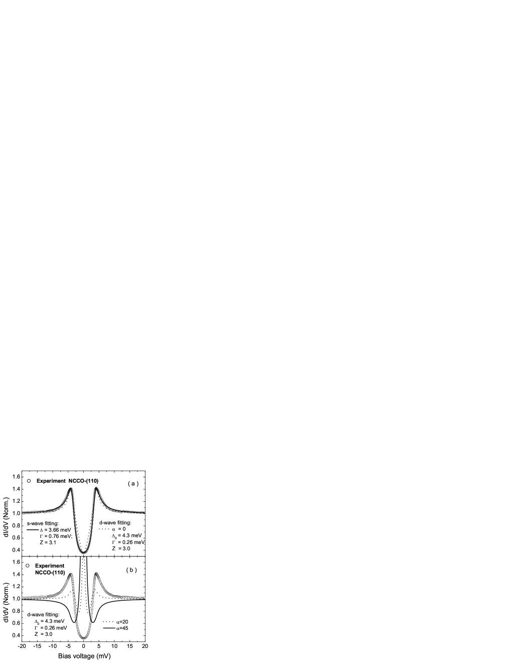
As discussed above, if the superconducting NCCO has -wave pairing symmetry, a ZBCP should be observed in the (110)-oriented tunneling spectrum. In other words, our experimental results suggest that the optimally doped NCCO has a -wave symmetry. In order to explain this viewpoint, we present in Fig. 7 the best fitting of the (110)-oriented tunneling spectrum with the formulas corresponding -wave and -wave models respectively. For the simulations, the extended BTK model BlonderGE1982 ; TanakaY1995 was accepted by selecting a constant gap value for -wave symmetry and the anisotropic gap of for symmetry, where is the polar angle measured from the crystallographic axis . In this model, two parameters are introduced to describe the necessary physical quantities, i.e., the effective potential barrier () and the superconducting energy gap (). As an extension, the quasiparticle energy is replaced by , where is the broadening parameter characterizing the finite lifetime of the quasiparticles due to inelastic scattering near the N/S micro-constriction DynesRC1984 ; PlecenA1994 . In a real N-I-S junction configuration, total tunneling conductance spectrum includes the integration over the solid angle. In the case of two dimension, it reduces to the integration over the injection angle from to , as done in this work. Fig. 7(b) clearly shows that the -wave theoretical simulation along the (110) direction deviates from the experimental data. When the normal direction of the sample surface departs a small angle from the crystallographic axis , a ZBCP will appear, accompanied by the remarkable depression of the coherence peaks. As shown in Fig. 7(a), even the -wave simulation absolutely along (100) direction can not fit the experimental data in the range below superconducting gap. However, the calculated curves in terms of the -wave theory are in good agreement with the experimental results both in (100) and (110) directions.
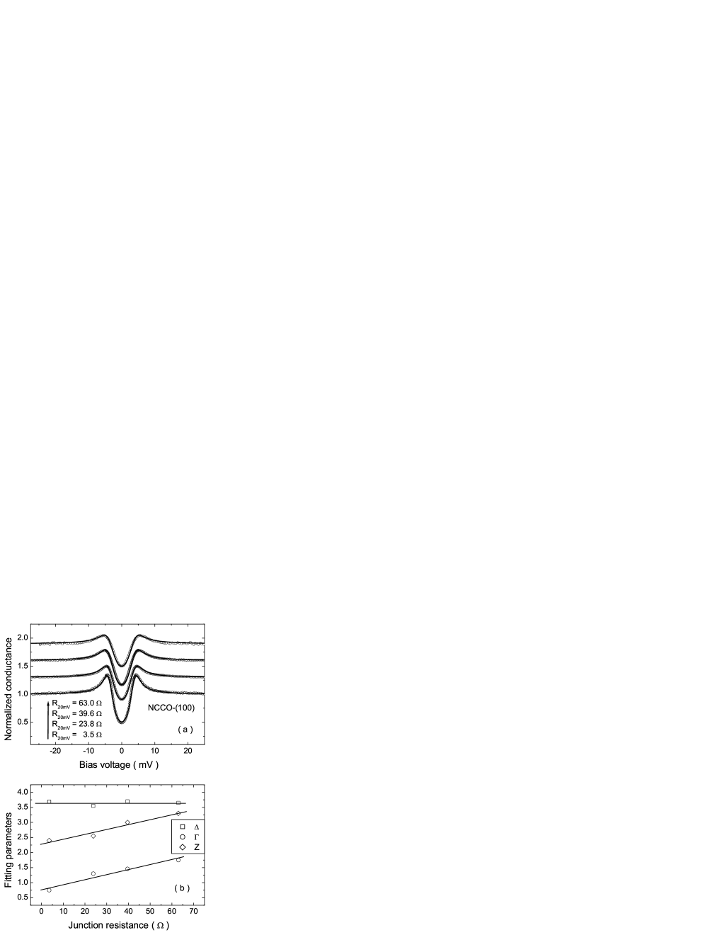
It should be pointed out that the values of and are related to the selected form of the background (such as the slope coefficient of the high bias straight-line segments) in a certain extent, which may be the main artificial uncertainty in the data analysis. So we did not focus our attention on the absolute values of these parameters or the quantitative comparison between the different spots. However, it is also found that the energy gap is insensitive to the selection of different background in the fitting process. Moreover, when we chose a general procedure to construct the background for all spectra measured on a fixed spot on the sample surface, the variation of the fitting parameters of and should be physically meaningful. As an example, we presented in Fig. 8(a) the normalized spectra measured at a fixed spot with different junction resistance, which have been theoretically fitted to the -wave BTK model and the fitting parameters are shown in Fig. 8(b). It is noted that the derived energy gap is nearly constant for all spectra, while the barrier height and broadening parameter continuously decreases with the decreasing junction resistance. This is physically reasonable and in good agreement with the foregoing discussions, namely, the abrasion of the contaminant layer will depress the barrier height accompanied by the weakening of the quasiparticle scattering near the N/S micro-constriction.


The good spatial repeatability of the tunneling spectra allowed further investigations on their temperature dependence. The spectral shape change continuously until above 24K (), thus suggesting that the tunneling spectra reflect the bulk superconductivity of the NCCO sample (Fig. 2(a)). The temperature dependent normalized spectra for both (110) and (100) directions are presented in Fig. 9, accompanied by the -wave BTK fitting curves denoted by the red solid lines. Because the spectra were affected by the critical current effect at higher temperature near SheetG2004 , it is difficult to determine the background for these temperatures. Therefore, these results have not been included in our theoretical analysis. All the parameters of the simulations shown in Fig. 9 are presented in Fig. 10 (the barrier height and the broadening parameter ) and Fig. 11 (superconducting energy gap ). The junction resistances measured at 20mV () are also given in Fig. 10.
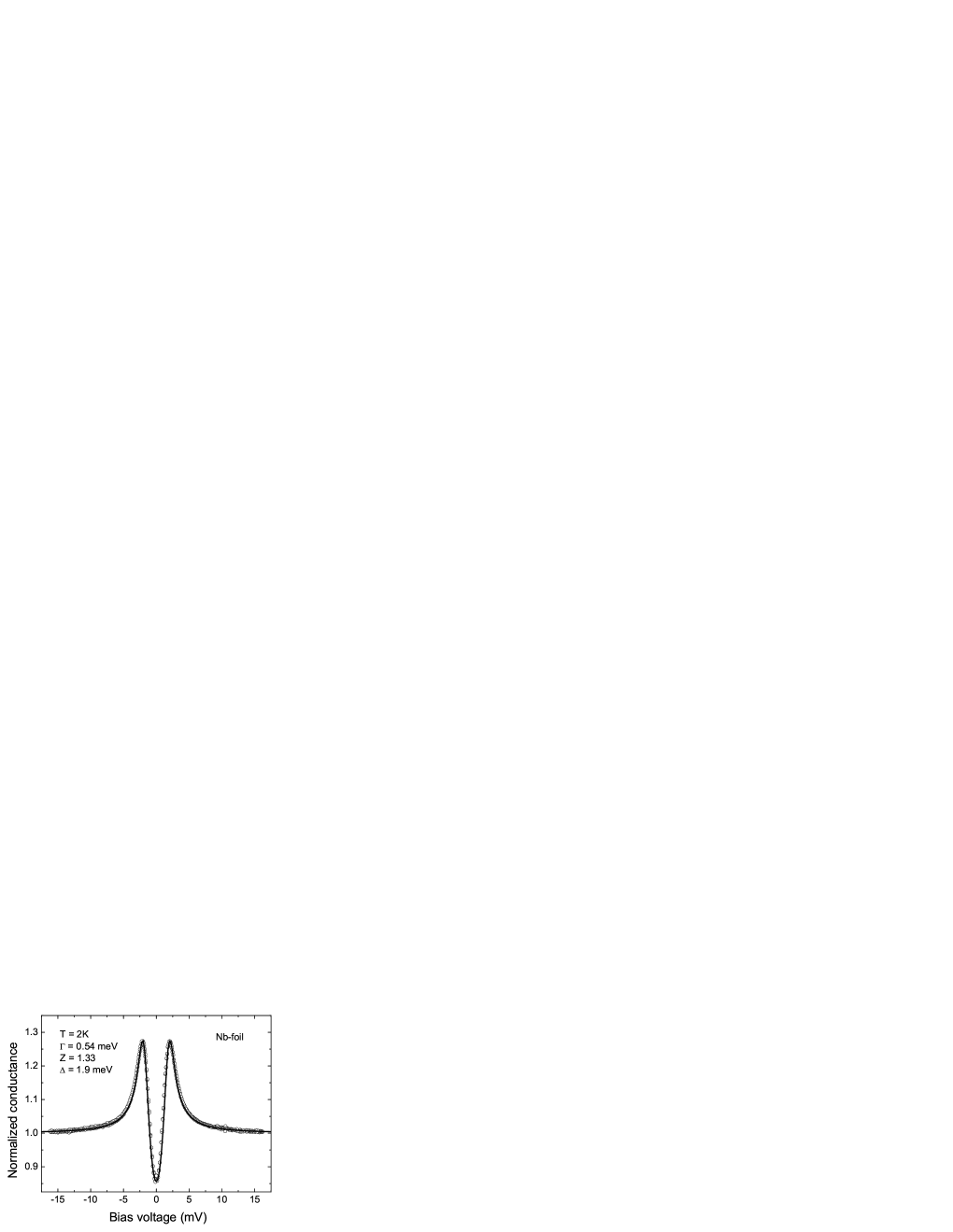
The magnitude of presented is larger than that of the clean point-contact junction between normal metal and conventional superconductors which in general is smaller than . However, considering the much shorter coherence length and faster exterior degradation of cuprates than that of the conventional superconductors, one can easily understand the larger . Actually, a large () is often obtained on the oxidized surface of Nb foil, a typical conventional superconductor, as shown in Fig. 12. The lowest value of achieved in this work is much smaller than the previous report of by STM measurements on NCCO single crystal KashiwayaS1998 .
As shown in Fig. 11, the normalized gap function determined by the fitting procedure can be well described by BCS theory, yielding a gap ratio , which is very close to the theoretical value of . Such consistency between the tunneling data of cuprates and the theoretical model over a wide temperature range (between 0K and ) is surprising. In order to determine the repeatability of such temperature dependent measurements, we plot in Fig. 11 two relations obtained at two different positions for the (110) direction. All the functions obtained along both (110) and (100) directions and from different positions follow the BCS theory in a normalized scale. The values derived from this figure is between 24.5K26K, near the bulk transition temperature .

The distribution of the superconducting energy gap derived from the spectral measurements at many different positions are shown in Fig. 13. There is no obvious difference between the data obtained from (110) and (100) directions. The value of varies in a narrow range from 3.50 to 3.70, indicating the good homogeneity of the superconductivity in the investigated regions.

III.3 Tunneling spectra of La1.89Sr0.11CuO4 (LSCO)
As a comparison, the directional tunneling spectra along both (100) and (110) directions were also studied on the LSCO single crystal, which has a typical -wave pairing symmetry (as checked recently by specific heat WenHH2004 ). The measured spectra at various temperatures are presented in Fig. 14. For the (100) direction at low temperatures, two clear coherence peaks appear in the spectra and no ZBCP can be observed. While for the (110)-oriented spectra, a prominent ZBCP was observed, accompanied by the disappearance of the coherence peaks. With the increasing temperature, all these characteristics become weaker and weaker and eventually vanish around . As mentioned above, photoemission experiments have proved that surface degradation resulting from air exposure form orders of magnitude faster on LSCO than NCCO, due to the existence of reactive alkaline earth elements in LSCO VasquezRP1994 . Therefore, the surface of LSCO degraded quickly before being put into the helium gas environment, which directly affected the subsequent spectral measurements. That is, the injecting quasiparticles felt strong scattering effect from the surface barrier layer (resulting in a very large spectral broadening factor), i.e., the measured spectra were badly smeared. As shown in Fig. 14, the superconducting characteristics nearly completely disappear above 20K which is much lower than the bulk critical temperature .

In order to further demonstrate the spectral differences along the two directions, the spectra of K have been normalized using the higher bias backgrounds, as shown in Fig. 15. Although the strong scattering effect has severely smeared the spectra and made the quantitative analysis difficult, the coherence peaks around gap energy are depressed and a ZBCP appears when the tunneling direction changes from (100) to (110) as expected from the -wave theory. These spectra are also consistent with the results obtained on the La2-xSrxCuO4/Ag junctions fabricated using a ramp-edge technique MiyakeT2003 .
III.4 Theoretical model - Anisotropic -wave and two-band model
In this section, we try to explain our experimental data with other possible models. In Ref.KashiwayaS1998 , the authors ascribed the unphysically large () to the unreasonable assumption of isotropic -wave symmetry. They found that if the maximum value of was assumed to be 0.2 similar to YBCO, reasonable fitting is obtained by assuming anisotropic -wave symmetry, namely, . Comparing this previous report with present work, we find that the large value of is mainly due to the surface degradation. Nonetheless, the anisotropic -wave symmetry seems to be reasonable considering the crystallographic symmetry and the topology of Fermi surface (FS) of NCCO KingDM1993 ; YuanQS2004 . In Fig. 16(a), the best fitting to such anisotropic -wave model is presented for both (110) and (100) directions. Recently, the ARPES experiment revealed another form of the gap function described as . Such function has also been tried in our fittings as shown in Fig. 16(b). All the parameters for the theoretical simulations of Fig. 16 are listed in Table 2. It is found that the isotropic -wave is the best candidate among the three -wave models mentioned above.
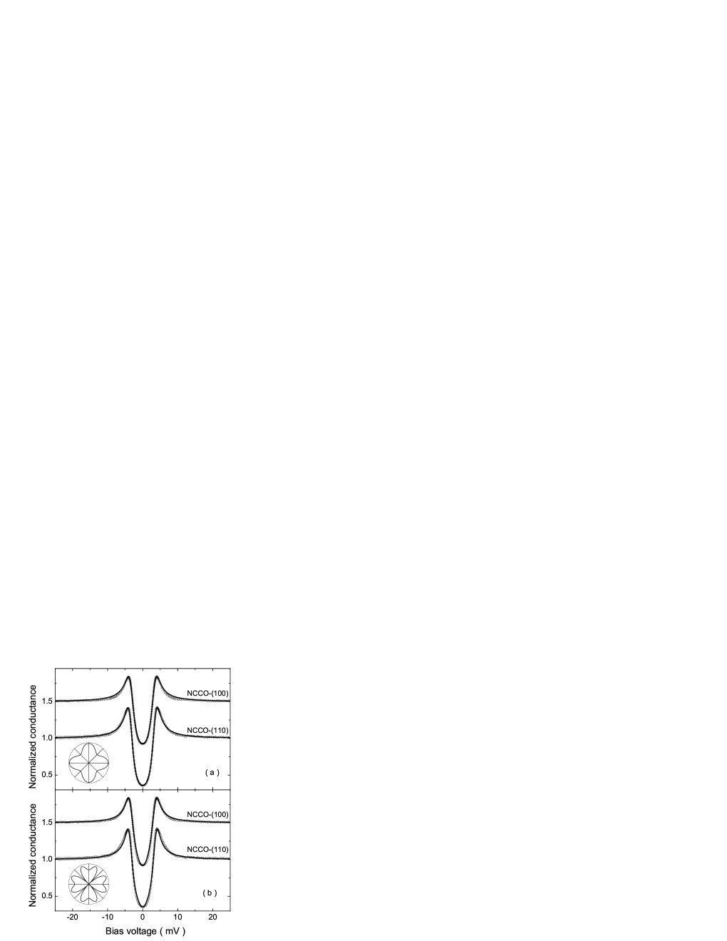
| Label | (meV) | (meV) | (meV) | ||
|---|---|---|---|---|---|
| (a)-(110) | 3.58 | 0.46 | 2.95 | 0.68 | 0.17 |
| (a)-(100) | 3.45 | 0.44 | 2.80 | 0.84 | 0.21 |
| (b)-(110) | 4.50 | None | 3.20 | 0.54 | 0.12 |
| (b)-(100) | 4.30 | None | 3.10 | 0.64 | 0.15 |
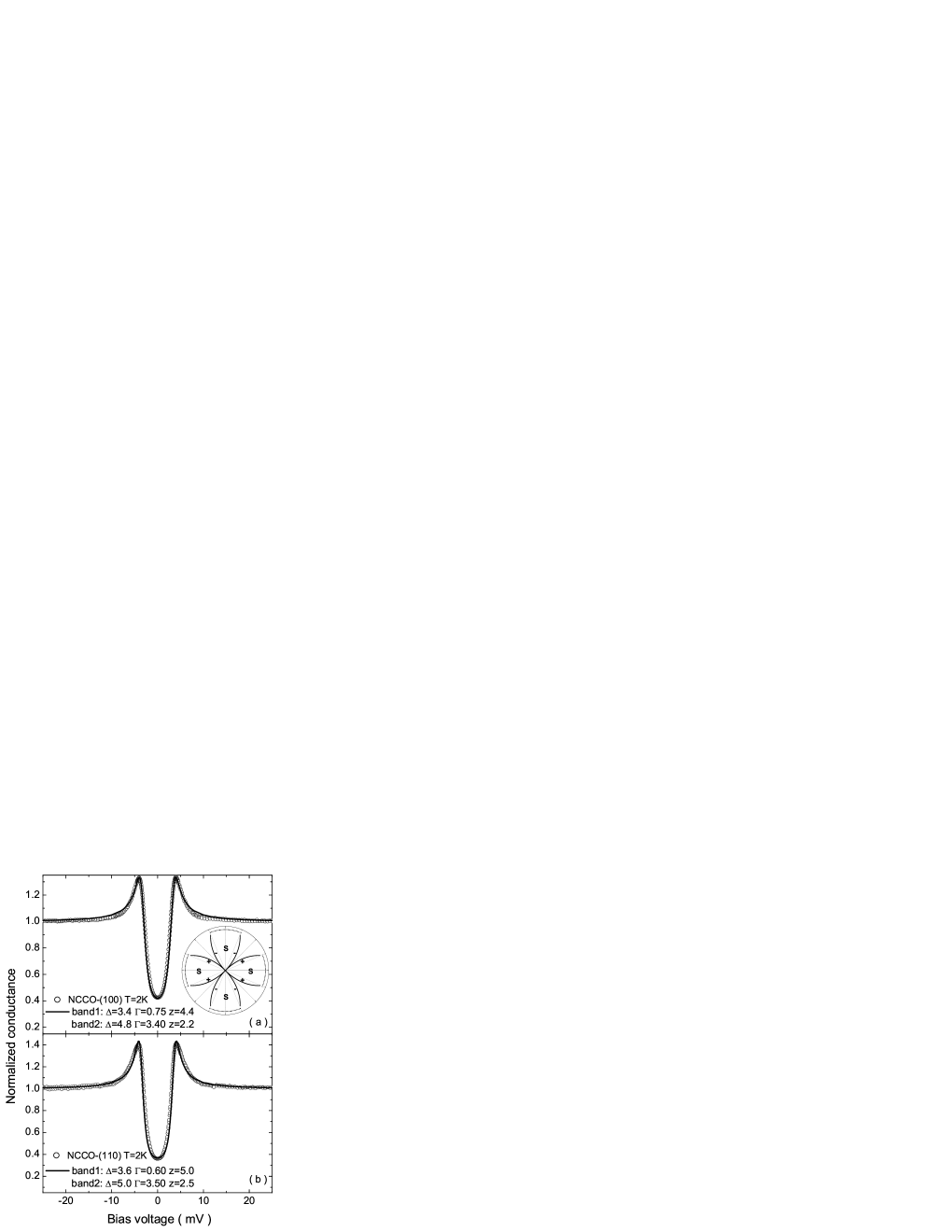
Recent ARPES experiments ArmitageNP2002 ; DamascelliA2003 revealed the doping evolution of the Fermi surface (FS) in Nd2-xCexCuO4. At low doping, a small Fermi pocket appears around (,0). Upon increasing doping, another pocket begins to form around (,) and eventually at optimal doping several FS pieces evolve into a large curve around (,). These findings were effectively described as a two-band system YuanQS2004 . Most recently, Luo et al. used a weakly coupled two-band BCS-like model to account for the low energy electromagnetic response of superconducting quasiparticles in electron-doped materials LuoHG2004 . The special angle dependence of the energy gap observed in Ref.MatsuiH2004 (as shown in the inset of Fig. 16(b)) may be a reflection of the two-band model. In the analysis in Ref.LuoHG2004 , both the pairing symmetries of band-1 and band-2 are assumed to be the type in order to achieve the best fitting for the superfluid density data, in which the labels 1 and 2 represent the bands contributing to the FS centered at (,0), (0,) and (,), respectively. However, as pointed out by the authors, there is a finite excitation gap in band-1 since the nodal lines do not intersect with the FS of that band if the system is not heavily overdoped. This indicates that the superconducting state of NCCO is actually a mixture of -wave and -wave-like pairing states. In other words, this analysis can not definitely determine whether the pairing symmetry of band-1 is -wave or -wave type. Based on this two-band model, we calculated the directional tunneling spectra by assuming different pairing symmetries (-wave or -wave) for band-1 while definite for band-2. In these calculations, the ratio of the contribution from band-1 to that from band-2 was chosen according to the discussions in Ref.LuoHG2004 . If only the -wave symmetry of band-1 is accepted, a prominent ZBCP will appear in the spectra along (110) direction. That is, the -wave symmetry of band-1 is required in the fitting procedure. Moreover, the best fitting needs a much larger value of for band-2 than that for band-1 as shown in Fig. 17, possibly due in part to the strong depression of the -wave superconductivity on the sample surface while the essential origin is yet to be found. Such mixture of superconductivity coming from two bands may be another possible reason of the contradicting reports on the pairing symmetry by different experiments. For example the phase sensitive measurements TsueiCC2000PRL ; Chesca may selectively detect the gap information from band-2 which crosses the Fermi surface near (). In addition, such inter-band mixture may also be responsible to the doping dependent pairing symmetry observed in thin films BiswasA2002 . In any case, the -wave pairing symmetry appears to be an important component in the superconductivity of optimally-doped NCCO.
In summary, the directional tunnelling spectra along (110) and (100) axis on the NCCO and LSCO single crystals illustrate clearly distinct pairing symmetries. In contrast to the results of LSCO (x=0.11), no ZBCP was observed for NCCO (x=0.15) along the two different directions while sharp coherence peaks are existent for both directions, which disagrees with the pure -wave pairing symmetry. The almost identical spectral shapes for the two directions on NCCO can be understood in the framework of -wave BTK theory, leading to a BCS type temperature dependence of energy gap with the ratio of . The present work provides evidence for the -wave component in the superconductivity of the optimally-doped NCCO, which should mainly come from the band crossing the FS around (,0) and (0,) if a two-band model is accepted.
Acknowledgements.
The authors thank Professor T.Xiang and Dr. H.G.Luo for fruitful discussions. The work is supported by the National Science Foundation of China, the Ministry of Science and Technology of China, and Chinese Academy of Sciences with the Knowledge Innovation Project. Pengcheng Dai is supported by the U. S. NSF DMR-0139882, DOE No. DE-AC05-00OR22725 with UT/Battelle, LLC., and by NSF of China under contract No. 10128408. We thank Dr. Y.G.Shi for the provision of some chemicals.E-mail address: hhwen@aphy.iphy.ac.cn (H. H. Wen); shanlei@ssc.iphy.ac.cn (L. Shan)
References
- (1) J. Orenstein and A. J. Millis, Science 288, 468 (2000).
- (2) Y. Tokura, H. Takagi, and S. Uchida, Nature 337, 345 (1989).
- (3) For a review see for example C. C. Tsuei and J. R. Kirtley, Rev. Mod. Phys. 72, 969 (2000) and references therein.
- (4) N. P. Armitage, D. H. Lu, D. L. Feng, C. Kim, A. Damascelli, K. M. Shen, F. Ronning, Z.-X. Shen, Y. Onose, Y. Taguchi, and Y. Tokura Phys. Rev. Lett. 86, 1126 (2001); T. Sato, T. Kamiyama, T. Takahashi, K. Kurahashi, and K. Yamada, Science 291, 1517 (2001).
- (5) Hamza Balci, V. N. Smolyaninova, P. Fournier, Amlan Biswas, and R. L. Greene, Phys. Rev. B 66, 174510 (2002).
- (6) C. C. Tsuei and J. R. Kirtley, Phys. Rev. Lett. 85, 182 (2000).
- (7) B. Chesca et al., Phys. Rev.B 71, 104504 (2005).
- (8) J. David Kokales, Patrick Fournier, Lucia V. Mercaldo, Vladimir V. Talanov, Richard L. Greene, and Steven M. Anlage, Phys. Rev. Lett. 85, 3696 (2000); R. Prozorov, R. W. Giannetta, P. Fournier, and R. L. Greene, Phys. Rev. Lett. 85, 3700 (2000).
- (9) A. Snezhko, R. Prozorov, D. D. Lawrie, R. W. Giannetta, J. Gauthier, J. Renaud, and P. Fournier, Phys. Rev. Lett. 92, 157005 (2004).
- (10) G. Blumberg, A. Koitzsch, A. Gozar, B. S. Dennis, C. A. Kendziora, P. Fournier, and R. L. Greene, Phys. Rev. Lett. 88, 107002 (2002).
- (11) H. Matsui, K. Terashima, T. Sato, T. Takahashi, M. Fujita, and K. Yamada, cond-mat/0411547.
- (12) C.-T. Chen, P. Seneor, N.-C. Yeh, R. P. Vasquez, L. D. Bell, C. U. Jung, J. Y. Kim, Min-Seok Park, Heon-Jung Kim, and Sung-Ik Lee, Phys. Rev. Lett. 88, 227002 (2002).
- (13) S. Kashiwaya, T. Ito, K. Oka, S. Ueno, H. Takashima, M. Koyanagi, Y. Tanaka, and K. Kajimura, Phys. Rev. B 57, 8680 (1998).
- (14) Z. Y. Liu, H. H. Wen, L. Shan, H.P. Yang, X. F. Lu, H. Gao, C.U. Jung, J. Y. Kim, Min-Seok Park, Heon-Jung Kim, and Sung-Ik Lee, Europhys. Lett. 69, 263 (2005).
- (15) L. Alff, S. Meyer, S. Kleefisch, U. Schoop, A. Marx, H. Sato, M. Naito, and R. Gross, Phys. Rev. Lett. 83, 2644 (1999).
- (16) John A. Skinta, Thomas R. Lemberger, T. Greibe, and M. Naito, Phys. Rev. Lett. 88, 207003 (2002).
- (17) M.-S. Kim, J. A. Skinta, T.R. Lemberger, A. Tsukada, and M. Naito, Phys. Rev. Lett. 91, 087001 (2003).
- (18) J. A. Skinta, M.-S. kim, T. R. Lemberger, T. Greibe, and M. Naito, Phys. Rev. Lett. 88, 207005 (2002).
- (19) A. Biswas, P. Fournier, M. M. Qazilbash, V. N. Smolyaninova, Hamza Balci, and R. L. Greene, Phys. Rev. Lett. 88, 207004 (2002).
- (20) H. Balci and R. L. Greene, Phys. Rev. Lett. 93, 067001 (2004).
- (21) Y. Onose, Y. Taguchi, K. Ishizaka, and Y. Tokura, Phys. Rev. Lett. 87, 217001 (2001).
- (22) F. Zhou, W. X. Ti, J. W. Xiong, Z. X. Zhao, X. L. Dong, P. H. Hor, Z. H. Zhang, and W. K. Chu, Supercond. Sci. Technol. 16, L7 (2003).
- (23) L. Shan, H. J. Tao, H. Gao, Z. Z. Li, Z. A. Ren, G. C. Che, and H. H. Wen, Phys. Rev. B 68, 144510 (2003).
- (24) R. P. Vasquez, B. D. Hunt, and M. C. Foote, Appl. Phys. Lett. 53, 2692 (1988).
- (25) Shao-Xiong Li, Hong-Jie Tao, Yi Xuan, Bo-Ru Zhao, and Zhong-Xian Zhao, Appl. Phys. Lett. 76, 3466 (2000).
- (26) R. P. Vasquez, J. Electron. Spectrosc. Relat. Phenom. 66, 209 (1994).
- (27) G.E. Blonder, M. Tinkham, and T.M. Klapwijk, Phys. Rev. B 25, 4515 (1982).
- (28) G.E. Blonder and M. Tinkham, Phys. Rev. B 27, 112 (1982).
- (29) S. Kashiwaya, N. Matsubara, B. Prijamboedi, H. Shibata, K. Takita, H. Kashiwaya, Y. Asano, and Y. Tanaka, J. Low Temp. Phys. 131, 327 (2003).
- (30) A. Mourachkine, Europhys. Lett. 50, 663 (2000).
- (31) Chia-Ren Hu, Phys. Rev. Lett. 72, 1526 (1994).
- (32) Y. Tanaka and S. Kashiwaya, Phys. Rev. Lett. 74, 3451 (1995); Phys. Rev. B 53, 9371 (1996).
- (33) S. Kashiwaya and Y. Tanaka, Rep. Prog. Phys. 63, 1641 (2000).
- (34) R. C. Dynes, J. P. Garno, G. B. Hertel, and T. P. Orlando, Phys. Rev. Lett. 53, 2437 (1984).
- (35) A. Pleceník, M. Grajcar, S. Benacka, P. Seidel and A. Pfuch, Phys. Rev. B 49, 10016 (1994).
- (36) G. Sheet, S. Mukhopadhyay, and P. Raychaudhuri, Phys. Rev. B 69, 134507 (2004).
- (37) H. H. Wen, Z. Y. Liu, F. Zhou, J. W. Xiong, W. X. Ti, T. Xiang, S. Komiya, X. F. Sun, and Y. Ando, Phys. Rev. B 70, 214505 (2004).
- (38) T. Miyake, T. Imaizumi, and I. Iguchi, Phys. Rev. B 68, 214520 (2003).
- (39) D. M. King, Z. X. Shen, D. S. Dessau, B. O. Wells, W. E. Spicer, A. J. Arko, D. S. Marshall, J. DiCarlo, A. G. Loeser, C. H. Park, E. R. Ratner, J. L. Peng, Z. Y. Li, and R. L. Greene, Phys. Rev. Lett. 70, 3159 (1993).
- (40) Qingshan Yuan, Yan Chen, T. K. Lee, and C. S. Ting, Phys. Rev. B 69, 214523 (2004).
- (41) N. P. Armitage, F. Ronning, D. H. Lu, C. Kim, A. Damascelli, K. M. Shen, D. L. Feng, H. Eisaki, Z. X. Shen, P. K. Mang, N. Kaneko, M. Greven, Y. Onose, Y. Taguchi, and Y. Tokura, Phys. Rev. Lett. 88, 257001 (2002).
- (42) A. Damacelli, Z. Hussain, and Z. X. Shen, Rev. Mod. Phys. 75, 473 (2003).
- (43) H. G. Luo and T. Xiang, Phys. Rev. Lett. 94, 027001 (2005).