Sharp bends in photonic crystal waveguides as nonlinear Fano resonators
Abstract
We demonstrate that high transmission through sharp bends in photonic crystal waveguides can be described by a simple model of the Fano resonance where the waveguide bend plays a role of a specific localized defect. We derive effective discrete equations for two types of the waveguide bends in two-dimensional photonic crystals and obtain exact analytical solutions for the resonant transmission and reflection. This approach allows us to get a deeper insight into the physics of resonant transmission, and it is also useful for the study and design of power-dependent transmission through the waveguide bends with embedded nonlinear defects.
I Introduction
Photonic crystals (PCs) are artificial dielectric structures with a periodic modulation in the refractive index that create a range of forbidden frequencies called a photonic band gap jdjprvsf97 . The existence of the photonic band gap can change dramatically the properties of the light allowing the realization of ultra-compact and multi-functional optical devices. One of the most fascinating properties of photonic crystals is their ability to guide electromagnetic waves in the narrow waveguides created by a sequence of line defects, including light propagation through extremely sharp waveguide bends with nearly perfect power transmission amjcciksfprvjdj96 ; sylecvhprvjdj98 . It is believed that the low-power reflection of sharp waveguide bends in photonic crystals is one of the most promising approaches to combine several devices inside a compact nanoscale optical chip.
The main advantage in achieving low radiation losses for the light transmission through sharp waveguide bends is based on the existence of the photonic band gap allowing to confine light inside a narrow defect waveguide due to the effect of the resonant Bragg scattering, reducing only the reflection losses of the bend design. Recent studies addressed the issue of an improved design of the sharp waveguide bends in two-dimensional photonic crystals and suggested that the transmission losses can be less then amjcciksfprvjdj96 ; acsn00 ; rleruafpmjsrmoj01 ; ecsyljrwsgjjdj01 ; sohbcwcjmstfkrhuo02 ; jschde03 ; zylkmh03 ; atmacmsmmsaphl04 ; jsjos04 ; inpprmdlr04 ; nm04 . However, most of those studies are based on direct numerical simulations and neither provide a deep understanding of the physics of the enhanced transmission of the sharp waveguide bends nor suggest simple approaches to design the waveguide bends with required transmission properties.
The main purpose of this paper is twofold. First, we demonstrate that transmission of electromagnetic waves through sharp bends of photonic crystal waveguides can be described by a simple discrete model where the waveguide bend plays a role of a specific localized defect. By employing the semi-analytical approach based on the Green’s function formalism sfmyskras00 ; sfmysk02 ; sfmusk02 , we derive effective discrete equations which allow us to describe the bend transmission as a special case of the so-called Fano resonance uf61 , recently discussed for the wave propagation in discrete chains aemsfmsfyusk05 . We demonstrate how to introduce the effective discrete model for the Fano resonance by selecting two common designs of the waveguide bends in two-dimensional photonic crystals created by a lattice of rods, and obtain exact analytical solutions for the resonant transmission and reflection. We show that asymmetric shapes of the transmission curves observed for the waveguide bends can be understood in terms of the Fano resonance which originates from the interaction between continuum waves and an effective localized state associated with the waveguide bend that provides an additional propagation channel for the wave transmission and, therefore, leads to the constructive or destructive interference. Second, we show that this approach allows us not only get a deeper physical insight but it is also useful to study the nonlinear transmission through the waveguide bends with nonlinear defects.
The paper is organized as follow. In Section 2 we derive the effective discrete equations for the case of two-dimensional photonic crystal waveguides based on the Green’s function technique. We employ the approach earlier suggested by Mingaleev et al. sfmyskras00 ; sfmysk02 ; sfmusk02 , but take into account the effect of the long-range interaction only in the vicinity of the waveguide bend. This allows us to derive an effective discrete Fano model where the waveguide bend plays a role of a special localized defect, and also suggest an effective way for predicting and controlling the properties of different types of the waveguide bends. Using this model, in Section 3 and Section 4 we study the wave transmission in the linear and nonlinear regimes, respectively. Section 5 concludes the paper.
II Effective discrete model
First, we derive an effective discrete model for the wave transmission through a sharp waveguide bend by employing and modifying the conceptual approach suggested earlier by Mingaleev et al. sfmyskras00 ; sfmysk02 . We consider a two-dimensional photonic crystal created by a square lattice (with the period ) of dielectric rods in air (). The rods have the radius and the dielectric constant . We study in-plane light propagation in this photonic lattice described by the electric field polarized parallel to the rods, and reduce the Maxwell’s equations to the scalar eigenvalue problem
| (1) |
For given parameters, this square lattice of rods is known to possess a large TM band gap () between the frequencies and .
We create a waveguide by replacing some of the lattice rods by the defect rods with the radius , or simply by removing some rods of the lattice. To describe the structure with defects, we decompose the permittivity function into a sum of the periodic part and the defect-induced contribution, , and rewrite Eq. (1) in the integral form sfmyskras00 ,
| (2) |
where is the standard Green’s function. If the radius of the defect rod is sufficiently small, the electric field inside the rod is almost constant, and the integral (2) can be easily evaluated. This allows us to derive a set of discrete equations for the electric field
| (3) |
where
| (4) |
are the frequency-dependent effective coupling coefficients,
| (5) |
is the defect-induced change of the lattice dielectric function, where is the dielectric constant of the defect rod located at the site .
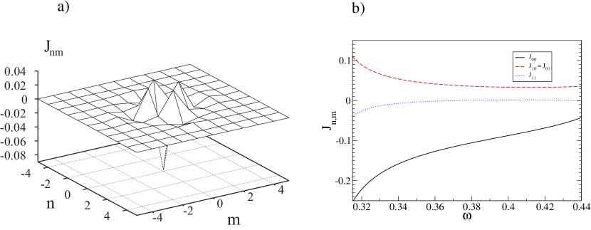
In general, the effective coupling coefficients decay slow in space, as shown in Fig. 1(a). This slow decay introduces effective long-range interaction (LRI) from site to site of the waveguide, which becomes crucially important for the waveguide bends. In reality, we define a finite distance of this (formally infinite) interaction by assuming that all coupling coefficients with the numbers and vanish. As demonstrated in Ref. sfmysk02 , the case gives already an excellent agreement with the results of the finite-difference time-domain numerical simulations.
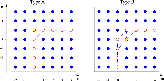
Unlike the previous studies of the effective discrete model, here we are interested in the light propagation through two types of the waveguide bends shown in Fig. 2 created by removed rods and additional defect rods with dielectric constant placed at the corner; the defect rod can also be nonlinear. Due to the effective long-range interaction, the corner in the bend waveguide can be considered as a special type of a defect; this resemblance is indeed correct and it explains the Fano-type resonances in the transmission as discussed below.
III Linear transmission
In this section, we consider the linear transmission through the waveguide bends when all corner defects are assumed to be linear. In order to show analytically that the waveguide bend generates an effective defect state and it can be described by a discrete model of the Fano resonance, we proceed in two steps making simplifications in the general model (3). For simplicity, we consider the waveguide bend of the type A, as shown in Fig. 2.
As the first step, we reduce the effective length of the long-range interaction in the straight parts of the waveguide bend taking it as . This approximation corresponds to the familiar tight-binding approximation that takes into account only the coupling between the nearest neighbors in a discrete chain. However, we take into account the nonlocal coupling near the sharp bend, and this requires to introduce an additional coupling of two sites around the corner as shown in Fig. 2 for the bend of the type A. It turns out that this simple approximation allows us to describe qualitatively all important properties and the key physics of the waveguide bend.
To derive the effective discrete model corresponding to the bend design shown in Fig. 2 (left), we remove two semi-infinite rows of rods and write the dielectric function in the form,
| (6) |
At the corner of the waveguide bend, we place a defect rod with the dielectric constant . Equations (3) for the electric field inside the defect rods can be written explicitly as
| (7) | |||||
where and . Importantly, the resulting set of coupled equations present a discrete model that can be compared with the discrete models earlier studied in Ref. aemsfmsfyusk05 , for which the existence of the Fano resonance has been demonstrated analytically.
First two equations in the system (III) allow us to obtain the dispersion relation for the bend waveguide far away from the corner. Due to the symmetry of the photonic crystal, the coupling terms and coincide and, therefore, we obtain the waveguide dispersion in the form
| (8) |
where is the wavenumber for the waves propagating along the waveguide. Other equations in the system (III) allow us to calculate the transmission coefficient of the waveguide bend,
| (9) |
where we use the notations
| (10) |
Important information about the resonant transmission follows from the study of zeros of the transmission coefficient (9). Except for the band edges (), the transmission coefficient vanishes when , i.e. when
| (11) |
As the second step, we approximate the dependence of the coupling coefficients in the effective discrete model on the frequency , considering the specific results presented in Fig. 1(b). In the frequency interval , we find the following approximation
| (12) |
where is the frequency of a single embedded defect (in our case, ), and are constants ( and ). By substituting Eq. (12) into Eq. (11), we obtain the quadratic equation
| (13) |
which has two solutions
| (14) |
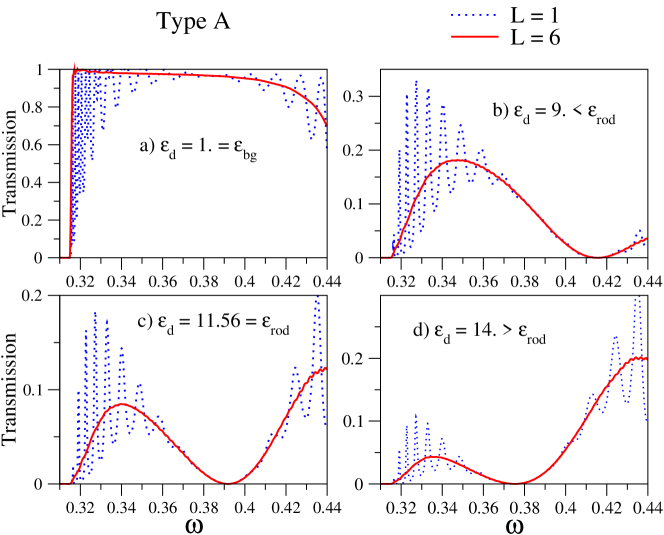
According to these results, there exists a possibility for two perfect reflections and, therefore, two Fano resonances. This is due to the linear frequency dependence of two coupling terms (12), the on-site term and the cross-coupling term . In our model, we have only one free parameter— the dielectric constant of the defect rod at the corner. Then, when at list one zero of the transmission lies inside the propagation spectrum (8), . As a result, we predict that when the perfect reflection through the waveguide bend of the type A should be observed, and numerical results confirm this prediction (see Fig. 3). We plot the transmission coefficient for two different values of the interaction, and . This shows that the tight-binding approximation () still gives reasonable results in average, and it works especially well near the Fano resonance where our model works nicely.
Both the effective model and calculation of the transmission coefficient for the waveguide bend of the type B (see Fig.2) are similar. The only difference between these two types of the bend design is the existence of additional coupling terms to the the defect state. As was shown in Ref. aemsfmsfyusk05 , by increasing the number of the coupling terms we only shift the position of the Fano resonance, either transmission or reflection. In our case, the coupling is small (), so that the renormalization is negligible. For the waveguide bend of the type A, the Fano resonance manifests itself as the perfect reflection only, whereas the perfect transmission lies outside the waveguide spectrum. By analyzing the transmission coefficient for the type B bend, we can show that in this case the perfect transmission may move to the waveguide spectrum when . This result coincides with the well-known result of the perfect transmission through the waveguide bend of the type B when the rod is removed at the corner, amjcciksfprvjdj96 ; sylecvhprvjdj98 .
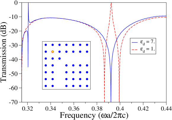
According to Fig. 3, by increasing the dielectric constant of the defect rod at the corner, we can achieve the perfect resonant reflection. However, the transmission itself becomes very low. However, it was shown in Ref. aemsfmsfyusk05 that when the coupling to the defect is very small the frequency of the perfect transmission is located very close to that of the perfect reflection; this results in a narrow and sharp Fano resonance. We employ this idea for the waveguide bend of the type A and replace one lattice rod by a defect rod outside the corner, as shown in the insert of Fig. 4. In this case, we obtain the perfect transmission for a particular frequency by varying the dielectric constant of the defect rod, see Fig. 4. Here, there exist two Fano resonances. One of them is broad, and it manifests itself as the perfect reflection only, being similar to the case of Fig. 3(c); it can be treated as the background transmission. The second resonance possesses a sharp asymmetric profile with both resonant transmission and reflection. Our analysis shows that for this design the so-called double Fano resonance can exists due to the specific frequency dependence of the coupling coefficients. By varying the dielectric constant of the defect rod placed outside the corner, we shift the asymmetric resonance whereas preserving the other one. When we simply remove the rod outside the corner (i.e. at ), these two resonances are located very close and interact with each other. As a result, the perfect transmission is accompanied by two perfect reflections, and this effect can be use to design a very efficient filter based on the bend waveguide transmission.
IV Nonlinear transmission
Finally, we apply our effective discrete model to the case of the nonlinear transmission through the waveguide bend with embedded nonlinear defect rods. In this case, we assume that the (green) defect rods placed at the bend corner (see Fig. 2) possesses a Kerr-type nonlinearity
| (15) |
For definiteness, in our numerical simulations we take the value and use the rescaled coefficient , these data should correspond to some polymer materials. In the nonlinear regime, the transmission of the waveguide bend depends on the intensity of the incoming light. This gives us an additional possibility to control the transmission properties of the waveguide bend by changing the properties of the nonlinear defect.
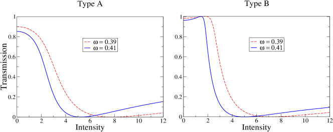
Our analysis shows that the presence of nonlinear defect does not remove the Fano resonance itself, but instead it shifts the position of the resonant frequency. As a result, we can tune the value of the resonant frequency by the input light intensity, the resonant scattering can be observed for almost all frequencies of the waveguide spectrum aemsfmsfyusk05 . Figure 5 shows the power-dependent transmission for two types of the waveguide bends with embedded nonlinear defects at the corner. For the type B bend, the perfect transmission is observed as well. The intensity-dependent transmission allows us to control the light propagation through the waveguide bend from up to by simply tuning the light intensity. From another hand, we can achieve transmission thought the type B bend for almost all frequencies from the spectral range by choosing a proper intensity of the incoming light.
V Conclusions
We have analyzed the conditions for high transmission through sharp waveguide bends using the effective discrete equations derived for two-dimensional photonic crystal waveguides. We have demonstrated that the physics of this effect can be understood with the help of a simple discrete model of the Fano resonance where the waveguide bend plays a role of a specific localized defect. Using this model, we have obtained exact analytical solutions for the resonant transmission and reflection of two types of the waveguide bends, in both linear and nonlinear regimes. We believe our approach would allow to get a deeper insight into the physics of resonant transmission through waveguide bends, and it can be useful for understanding other types of resonant effects in two- and three-dimensional photonic crystal waveguides and circuits.
The authors acknowledge useful discussions and collaboration with Sergei Mingaleev.
References
- (1) J. D. Joannopoulos, P. R. Villeneuve, and S. Fan, “Photonic crystals: putting a new twist on light”, Nature 386, 143-149 (1997).
- (2) A. Mekis, J.C. Chen, I. Kurland, S. Fan, P.R. Villeneuve, and J.D. Joannoppoulos, “High transmission through sharp bends in photonic crystal waveguides”, Phys. Rev. Lett. 77, 3787-3790 (1996).
- (3) S.-Y. Lin, E. Chow, V. Hietala, P. R. Villeneuve, and J. D. Joannopoulos, “Experimental demonstration of guiding and bending of electromagnetic waves in a photonic crystal”, Science 282, 274-276 (1998).
- (4) A. Chutinan and S. Noda, “Waveguides and waveguide bends in two-dimensional photonic crystal slabs”, Phys. Rev. B 62, 4488-4492 (2000).
- (5) R.L. Espinola, R.U. Ahmad, F. Pizzuto, M.J. Steel, and R.M. Osgood Jr.,“A study of high-index-contrast 90 degree waveguide bend structures”, Opt. Express 8, 517-528 (2001).
- (6) E. Chow, S. Y. Lin, J. R. Wendt, S. G. Johnson, and J. D. Joannoppoulos, “Quantitative analysis of bending efficiency in photonic-crystal waveguide bends at = 1.55 m wavelengths”, Opt. Lett. 26, 286-288 (2001).
- (7) S. Olivier, H. Benisty, C. Weisbuch, C. J. M. Smith, T.F. Krauss, R. Houdré, and U. Oesterle, “Improved 60 degree bend transmission of Ssubmicron-width waveguides defined in two-dimensional photonic crystals”, J. Lightwave Technol. 20, 1198-1203 (2002).
- (8) J. Smajic, C. Hafner, and D. Erni, “Design and optimization of an achromatic photonic crystal bend ”, Opt. Express 11, 1378-1384 (2003).
- (9) Z.Y. Li and K.M. Ho, “Light propagation through photonic crystal waveguide bends by eigenmode examinations” Phys. Rev. B 68, 045201 (12) (2003).
- (10) A. Talneau, M. Agio, C. M. Soukoulis, M. Mulot, S. Anand, and Ph. Lalanne,“High-bandwidth transmission of an efficient photonic-crystal mode converter”, Opt. Lett. 29, 1745-1747 (2004).
- (11) J. S. Jensen and O. Sigmund, “Systematic design of photonic crystal structures using topology optimization: Low-loss waveguide bends”, App. Phys. Lett. 84, 2022-2024 (2004).
- (12) I. Ntakis, P. Pottier, and R. M. De La Rue, “Optimization of transmission properties of two-dimensional photonic crystal channel waveguide bends through local lattice deformation”, J. App. Phys. 96, 12-18 (2004).
- (13) N. Malkova, “Tunable resonant light propagation through 90o bend waveguide based on strained photonic crystal”, J. Phys.: Cond. Matt. 16, 1523-1530 (2004).
- (14) S.F. Mingaleev, Yu.S. Kivshar, and R.A. Sammut,“Long-range interaction and nonlinear localized modes in photonic crystal waveguides”, Phys. Rev. E 62, 5777-5782 (2000).
- (15) S.F. Mingaleev and Yu.S. Kivshar, “Effective equations for photonic-crystal waveguides and circuits”, Opt. Lett. 27, 231-233 (2002).
- (16) S. F. Mingaleev and Yu. S. Kivshar, “Nonlinear transmission and light localization in photonic-crystal waveguides”, J. Opt. Soc. Am. B 19, 2241-2249 (2002).
- (17) U. Fano, “Effects of configuration interaction on intensities and phase shifts”, Phys. Rev. 124, 1866-1878 (1961).
- (18) A.E. Miroshnichenko, S.F. Mingaleev, S. Flach, and Yu.S. Kivshar, “Nonlinear Fano resonance and bistable wave transmission”, Phys. Rev. E 71 (2005) in press.
- (19) T. Zijlstra, E. van der Drift, M. J. A. de Dood, E. Snoeks, and A. Polman, “Fabrication of two-dimensional photonic crystal waveguides for 1.5 m in silicon by deep anisotropic dry etching”, J. Vac. Sci. Tech. B 17, 2734-2739 (1999).