Cotunneling-mediated transport through excited states
in the Coulomb blockade regime
Abstract
We present finite bias transport measurements on a few-electron quantum dot. In the Coulomb blockade regime, strong signatures of inelastic cotunneling occur which can directly be assigned to excited states observed in the non-blockaded regime. In addition, we observe structures related to sequential tunneling through the dot, occuring after it has been excited by an inelastic cotunneling process. We explain our findings using transport calculations within the real-time Green’s function approach, including diagrams up to fourth order in the tunneling matrix elements.
pacs:
73.23.Hk, 73.40.GkIn a quantum dot in the Coulomb blockade regime, the energy gap related to the charging energy becomes larger than and sequential tunneling transport involving only dot ground states is exponentially suppressed (see e.g. van Houten et al. (1992)). Transport is dominated by cotunneling Averin and Nazarov (1990). Elastic cotunneling, prevalent at low bias voltages, involves virtual tunneling of one electron through the dot via a higher-energy state and leaves the dot in the ground state. Inelastic processes imply correlated tunneling of two electrons, leaving the dot in an excited state with energy above the ground state. Inelastic cotunneling sets in once the bias energy . Recently, Golovach and Loss have presented a theoretical analysis of the interplay between cotunneling and sequential tunneling in a double dot system Golovach and Loss (2004). Experimental investigations involving cotunneling have been performed on metallic Geerligs et al. (1990); Hanna et al. (1992); Eiles et al. (1992) and semiconducting Glattli et al. (1991); Pasquier et al. (1993); Cronenwett et al. (1997) systems containing a large number of electrons. Signatures of inelastic cotunneling in a transport measurement have been observed in investigations on small vertical semiconductor quantum dots De Franceschi et al. (2001); Yamada et al. (2003), and in single-walled Nygard et al. (2000) and multiwalled Buitelaar et al. (2002) carbon nanotubes, all containing well separated energy levels.
In the following, we first present finite bias transport measurements through a quantum dot, showing structure outside as well as within the Coulomb blockade regime. In the second part, we present a theoretical analysis of our results based on transport calculations using the real-time Green’s function approach.
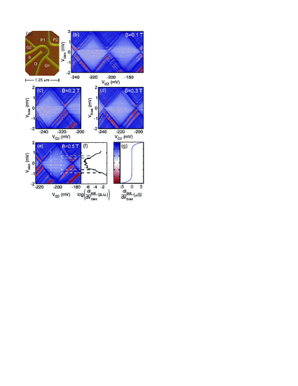
The sample (see Fig. 1(a)) was fabricated by surface probe lithography Held et al. (1999); Lüscher et al. (1999) on a GaAs/Al0.3Ga0.7As heterostructure, containing a two-dimensional electron gas (2DEG) below the surface as well as a backgate (BG) below the 2DEG. The unstructured 2DEG had a mobility of and a density of at a temperature and a BG voltage .
All measurements were performed in a dilution refrigerator with a base temperature of . Negative voltages were applied to the surrounding gates (see Fig. 1(a)) and to the back gate, to tune the charge on the dot and the transparency of its tunnel barriers. The bias voltage was applied symmetrically (with respect to ground) across the dot between source (S) and drain (D). The dc transport current was measured and numerically differentiated. An estimated charging energy and a single level spacing were extracted.
Figure 1 shows measurements of finite bias differential conductance on a strongly nonlinear scale. Figs. 1(b)-(e) contain measurements of differential conductance vs. both gate voltage and bias voltage. Measurements were performed at different magnetic fields in order to vary the wave functions inside the quantum dot and their coupling to the reservoirs. Inside the diamond-shaped regions, i.e. in the Coulomb blockaded regime, we observe horizontal (constant bias) structures. At the diamond boundary, the horizontal lines seamlessly join some of the most prominent diagonal lines in the non-blockaded region. In Figure 1(f), an averaged trace of the current vs. bias voltage is presented, showing the position of these kinks more precisely.
For positive bias, e.g. in Fig. 1(b), additional structure inside the diamond is observed: for bias voltages above the well-resolved horizontal threshold line, diagonal lines parallel to the diamond edges appear. In our measurements, this feature remains visible at all magnetic fields measured (from to in steps of , see Figs. 1(c)-(e) for more examples). The vertical distance between the diagonal lines and the diamond edge is identical for positively (left of diamond) and negatively sloped lines. When extended towards higher or towards negative voltages, most of the diagonal lines apparently join prominent lines in the non-blockaded regime.
A closer examination of the structures reveals a connection between two energy scales visible inside the blockaded region (see Figure 3(c) for an illustration): an extension of each diagonal line intersects the zero bias line at a certain point (point A in Fig. 3(c)). Connecting this point to the diamond edge at its intersection with the closest horizontal line (point B in Fig. 3(c)) yields an extension of a diagonal line (of opposite slope) in the non-blockaded regime. This remains valid at different magnetic fields, where the vertical distance between the diagonal line and the diamond edge varies by a factor of about 2.
While we observe the horizontal structures for at least 12 consecutive Coulomb blockade diamonds, the diagonal features are only seen for a maximum of two neighbouring diamonds up to now. On reducing the transparencies of the dot’s tunnel barriers, the amplitude of the cotunneling currents become comparable to the minimum current resolution, and the structures inside the Coulomb diamonds gradually disappear.
We interpret our findings as follows: the horizontal lines in the blockaded regime mark the onset of inelastic cotunneling connected to specific excited states. The distance from the zero-bias line corresponds to the single-particle level spacing of these states with respect to the ground state. At the intersection points at the border of the Coulomb diamonds, a direct mapping can be made of the excited states that contribute measurably to inelastic cotunneling and those that open additional transport channels in the non-blockaded, finite-bias regime. The horizontal line close to zero bias in Fig. 1(e) suggests the presence of a state with low excitation energy contributing to inelastic cotunneling.
The most unconventional features observed are the diagonal lines inside the Coulomb blockaded regions. The fact that they have the same slope as the diamond edges suggests that they are connected to the alignment of an energy level with source (negative slope) or drain (positive slope).
To verify this hypothesis, we have performed transport calculations within the real-time Green’s function approach Schoeller and Schön (1994a) including all cotunneling diagrams, i.e. all diagrams to fourth order in the tunneling matrix elements Tews (2004). In the following, the results for a quantum dot with a simple level structure are discussed.
The simplest quantum dot which shows signatures of its excitation spectrum in the Coulomb blockade regime is described by an Anderson Hamiltonian having two non-degenerate single-particle levels and and the excitation energy :
| (1) | |||||
| (2) |
The annihilation (creation) operator annihilates (creates) an electron of state in the quantum dot. Coulomb interaction is described by the second term of (2) leading to an additional interaction energy whenever the dot is occupied by two electrons. The four possible states of the isolated quantum dot are labeled as follows: denotes the empty dot, the single-particle ground state, the excited single-particle state, and the two-particle state. Here we assume that the applied gate voltage leads to a constant electrostatic potential described by the third term of the quantum dot Hamiltonian. In this term, is the number operator for the dot electrons and the electrostatic lever arm of the gate electrode. The coupling of the quantum dot to two reservoirs is described by the reservoir () and the tunneling Hamiltonian (). They are of the conventional form (see e.g. Tews (2004), Cohen et al. (1962)) with the reservoir electrons being treated as non-interacting except for an overall self-consistent potential Jauho (1998), owing to the high density of states in source and drain contacts. For simplicity, we assume for the following the absolute value of the complex tunneling matrix elements to be independent of all quantum numbers with a complex phase which is random with respect to the direction of the reservoir electrons wave vector.
In order to calculate the non-equilibrium transport properties for finite transport voltages , we use the real-time transport theory developed by Schoeller et al. Schoeller and Schön (1994a). Following the steps of this theory one can trace out the reservoir degrees of freedom and derive a formally correct equation of motion for the reduced density matrix of the quantum dot system which under steady state conditions transforms into
| (3) |
Here denotes a matrix element of the reduced dot density matrix with the (few)-particle states and of the isolated quantum dot. The kernel represents a generalized transition rate involving the relevant tunneling processes. Within the same formalism one can also calculate the tunneling current expectation value for the steady state
| (4) |
In the sequential tunneling approximation, a “tunneling in” process is only possible if a reservoir electron matches the energy required to charge the quantum dot by a further electron. Generally, this energy is given by for a transition between the state (where is the th -particle state) and the -particle state and is in the following called transport channel and denoted by . For the quantum dot described by (2), four transport channels exist. In the Coulomb blockade regime, where transport in lowest order is exponentially supressed, the electrochemical potentials of both reservoirs are in between the two transport channels associated with two groundstates: . Going one step further and calculating the kernel of (3) in fourth order, already 64 qualitativly different terms occur, describing so-called cotunneling processes in which two electrons participate coherently in a tunneling process. In the following we study the resulting differential conductance including consistently all cotunneling contributions 111An advantage of the real-time transport theory is that the kernel is well defined and can be expressed systematically order by order in the tunnel coupling strength ..
In Fig. 2(b) the differential conductance as a function of the applied source-drain voltage is shown within the Coulomb blockade regime, i.e., the electro-chemical potentials for are energetically in between the two ground state channels and .
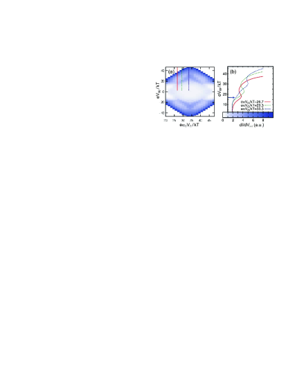
For small voltages, all three traces start with the same value and at least the traces for and stay constant for small transport voltages. This constant and finite differential conductance can be attributed to elastic cotunneling by virtual tunneling through either the vacuum or the two-particle state. Additionally, for all three traces a peak is found which shifts linearly to higher source-drain voltages with increasing gate voltage. In contrast to the traces at lower gate voltages, the differential conductance of the highest gate voltage () shows an additional step (see arrow in Fig. 2(b)) emerging at the source-drain voltage , which corresponds to the excitation energy . This step is strongly smeared due to temperature and especially due to the overlap with the peak occurring at higher voltages (also responsible for the strong increase towards higher bias voltages).
In Fig. 3(a), the relative position of the transport channels with respect to the electrochemical potentials in the reservoirs is shown at the
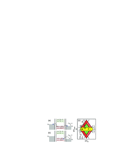
parameters where the step occurs ( and ). In this situation, inelastic cotunneling becomes possible in which the quantum dot becomes excited during the tunneling process. This additional (to the elastic process) cotunneling process leads to a step in the differential conductance Funabashi et al. (1999) which corresponds to the experimentally observed steps showing as horizontal lines in Fig. 1. Eventually, by further increasing the source-drain voltage , the electrochemical potential of the drain reservoir becomes resonant with the transport channel (sketched in Fig. 3(b)). Other than in the sequential tunneling approximation, where the state cannot be occupied due to the Coulomb blockade effect, inelastic cotunneling allows to occupy this excited state and the resonant channel leads to a peak in the differential conductance. Due to the smaller cotunneling rate, the peak is lower as compared to the corresponding peak beyond the Coulomb blockade regime.
For lower gate voltages, the peak moves to lower source-drain voltages and eventually merges with the step at . For even lower gate voltages, the channel is already within the transport window at the source-drain voltage needed to allow for the inelastic cotunneling process.
Combining all these processes, various tunneling regimes within the Coulomb blockade can be identified as sketched in Fig. 3(c). For , transport is dominated by elastic cotunneling, leading to a constant offset of the differential conductance. For gate-voltages in the vicinity of the Coulomb blockade center and , a regime where elastic and inelastic cotunneling occur is found. In the remaining outer regime, sequential tunneling through the excited single-particle state is also possible. At the border of this regime, a peak occurs in the differential conductance. All described features are also found in the calculated charging diagram including cotunneling (shown in Fig. 2(a)).
While it is not entirely clear to us why the induced sequential tunneling contributions have not been observed before, we can identify a few requirements: First of all, the charging energy has to be large enough, . This can be directly seen from Fig. 3(c), and it explains why the effect has not been observed e.g. in De Franceschi et al. (2001). In addition, a sufficient level spacing is required so that the effect is not smeared out by temperature. We speculate that the strongly asymmetric tunnel barrier configuration used in the present experiment may also enhance the visibility of these features.
Elastic cotunneling has earlier been identified as a possible source of uncertainty in the operation of single-electron devices (see e.g. Averin and Nazarov (1990)). Our results show that the inelastic contributions can become more prominent, especially if the induced sequential tunneling is taken into account. It follows that in an application relying on Coulomb blockade in quantum dots, e.g. in quantum information processing, the bias must be kept small in comparison to the lowest excitation energy.
We thank L. Kouwenhoven for valuable discussions. Financial support from the Swiss National Science Foundation and the NCCR “Nanoscale Science” is gratefully acknowledged. M.T. and D.P. acknowledge financial support of the Deutsche Forschungsgemeinschaft via SFB 508 “Quantum Materials”.
References
- van Houten et al. (1992) H. van Houten, C. W. J. Beenakker, and A. A. M. Staring, in Single Charge Tunneling: Coulomb blockade Phenomena in Nanostructures, edited by H. Grabert and M. H. Devoret (Plenum Press and NATO Scientific Affairs Division, New York, 1992), vol. 294 of NATO ASI Series, Series B: Physics, p. 167.
- Averin and Nazarov (1990) D. V. Averin and Y. V. Nazarov, Phys. Rev. Lett. 65, 2446 (1990).
- Golovach and Loss (2004) V. N. Golovach and D. Loss, Phys. Rev. B 69, 245327 (2004).
- Geerligs et al. (1990) L. J. Geerligs, D. V. Averin, and J. E. Mooij, Phys. Rev. Lett. 65, 3037 (1990).
- Hanna et al. (1992) A. E. Hanna, M. T. Tuominen, and M. Tinkham, Phys. Rev. Lett. 68, 3228 (1992).
- Eiles et al. (1992) T. M. Eiles, G. Zimmerli, H. D. Jensen, and J. M. Martinis, Phys. Rev. Lett. 69, 148 (1992).
- Glattli et al. (1991) D. C. Glattli, C. Pasquier, U. Meirav, F. I. B. Williams, Y. Jin, and B. Etienne, Z. Phys. B 85, 375 (1991).
- Pasquier et al. (1993) C. Pasquier, U. Meirav, F. I. B. Williams, D. C. Glattli, Y. Jin, and B. Etienne, Phys. Rev. Lett. 70, 69 (1993).
- Cronenwett et al. (1997) S. M. Cronenwett, S. R. Patel, C. M. Marcus, K. Campman, and A. C. Gossard, Phys. Rev. Lett. 79, 2312 (1997).
- De Franceschi et al. (2001) S. De Franceschi, S. Sasaki, J. M. Elzerman, W. G. Van-Der-Wiel, S. Tarucha, and L. P. Kouwenhoven, Phys. Rev. Lett. 86, 878 (2001).
- Yamada et al. (2003) K. Yamada, M. Stopa, T. Hatano, T. Ota, T. Yamaguchi, and S. Tarucha, Superlatt. Microstruct. 34, 185 (2003).
- Nygard et al. (2000) J. Nygard, D. H. Cobden, and P. E. Lindelof, Nature 408, 342 (2000).
- Buitelaar et al. (2002) M. R. Buitelaar, A. Bachtold, T. Nussbaumer, M. Iqbal, and C. Schönenberger, Phys. Rev. Lett. 88, 156801 (2002).
- Held et al. (1999) R. Held, S. Lüscher, T. Heinzel, K. Ensslin, and W. Wegscheider, Appl. Phys. Lett. 75, 1134 (1999).
- Lüscher et al. (1999) S. Lüscher, A. Fuhrer, R. Held, T. Heinzel, K. Ensslin, and W. Wegscheider, Appl. Phys. Lett. 75, 2452 (1999).
- Schoeller and Schön (1994a) H. Schoeller and G. Schön, Phys. Rev. B 50, 18436 (1994a).
- Tews (2004) M. Tews, Ann. Phys. 13, 249 (2004).
- Cohen et al. (1962) M. H. Cohen, L. M. Falicov, and J. C. Phillips, Phys. Rev. Lett. 6, 316 (1962).
- Jauho (1998) A. P. Jauho, in Theory of Transport Properties of Semiconductor Nanostructures, edited by Eckehard Schöll (Chapman and Hall, London, 1998).
- Funabashi et al. (1999) Y. Funabashi, K. Ohtsubo, M. Eto, and K. Kawamura, Jpn. J. Appl. Phys. 38, 388 (1999).