Electronic transport in quasi-one-dimensional arrays of gold nanocrystals
Abstract
We report on the fabrication and current-voltage (IV) characteristics of very narrow, strip-like arrays of metal nanoparticles. The arrays were formed from gold nanocrystals self-assembled between in-plane electrodes. Local cross-linking of the ligands by exposure to a focused electron beam and subsequent removal of the unexposed regions produced arrays as narrow as four particles wide and sixty particles long, with high degree of structural ordering. Remarkably, even for such quasi-one-dimensional strips, we find nonlinear, power-law IV characteristics similar to that of much wider two-dimensional (2D) arrays. However, in contrast to the robust behavior of 2D arrays, the shape of the IV characteristics is much more sensitive to temperature changes and temperature cycling. Furthermore, at low temperatures we observe pronounced two-level current fluctuations, indicative of discrete rearrangements in the current paths. We associate this behavior with the inherent high sensitivity of single electron tunneling to the polarization caused by the quenched offset charges in the underlying substrate.
pacs:
73.23.-b, 73.22.-f, 73.23.HkI Introduction
Metal or semiconductor nanoparticles and complex structures built from them through self-assembly whitesides ; redl ; lopes ; liao provide model systems for further investigation of physics on the mesoscopic scale, where quantum confinement and Coulomb charging set the relevant energy scales. imry Electronic properties of single particles vonDelft as well as two- and three-dimensional superlattices of nanocrystals gs ; bawendi ; parthasarathyIV have been extensively studied over the last decade. Here we address what happens to electronic transport as the one-dimensional limit is approached.
Electronic transport through an array of small metal particles separated by nanoscale gaps is determined by the interplay between single electron charging of an individual particle and tunneling between adjacent particles. In the presence of charge disorder due to quenched impurities in the insulating substrate under the array, middleton this interplay leads to highly non-Ohmic current-voltage IV characteristics. Theory and simulations predict that, at sufficiently low temperatures, no current flows below a voltage threshold, , while above it the current follows a power-law, , with in 1D and between 5/3 and 2 in 2D. middleton ; reichhardt ; rendell
Experimentally, true 1D chains are difficult to achieve and, so far, results have been obtained only on quasi-1D structures with significant amount of disorder in the particle arrangements. Narrow chains of carbon nanoparticles bezryadin showed sample-dependent scaling exponents between 1 and 2.3. Electron-beam written 100nm wide multilayers of particles clarke exhibited , and experiments on strips of 1.8nm gold clusters shirley gave . This spread in exponents is in sharp contrast with the situation for well-ordered, 2D Au monolayer nanocrystal arrays. Experiments on highly ordered 2D nanocrystal arrays found , a value that is temperature-independent and highly reproducible from sample to sample. parthasarathyIV ; parthasarathyTDep
These results highlight two key issues. First, to what extent is the spread in the measured scaling exponents caused by the charge disorder in (quasi-) 1D structures rather than to structural disorder and fabrication details; second, how narrow does an array have to be in order for its current-voltage characteristics to cross over from a nonlinear, 2D behavior to the a linear response with ? To address these issues, we performed systematic measurements on quasi-1D strips fabricated from well-ordered monolayer superlattices. These structures also allow us to observe explicitly the effects of quenched charges in the substrate through measuring the current fluctuation at fixed temperature and the changes in the current-voltage characteristics after temperature-cycling the array.
II Samples
Gold nanocrystals of 5.5nm diameter with 5-7% dispersity were synthesized as described in Ref. linSynthesis, through a digestive ripening method and suspended in toluene. A droplet of this colloidal suspension was then deposited onto -coated Si substrates with prefabricated, 15nm thick in-plane chromium electrodes ( wide with 500nm gap, i.e., about 60 particles across). By controlling the particle concentration, solvent evaporation rate and concentration of excess alkanethiol ligands in the solution, this drop drying procedure was used to form highly ordered nanocrystal monolayers. linOrder Alternatively, a water droplet was first deposited onto the substrate and the colloidal suspension was allowed to creep up at the water-air interface, forming a thin layer which then draped itself over the substrate as the water slowly evaporated. eah Both methods allow nanocrystals to self-assemble into a compact 2D monolayer at the liquid-air interface before the solvent dewetting occurs.
After solvent evaporation, the quasi-1D array was fabricated by exposing the corresponding monolayer regions to a finely focused electron beam in a scanning electron microscope (SEM). werts ; lohau ; linEBW Line doses of or area doses of were used to e-beam-write lines or rectangles at 30kV. These exposure parameters effectively cross-link the interstitial ligands but do not affect the nanoparticles’ shape and relative position. werts The exposed regions become resilient to heated toluene, which can be used to wash away unexposed particles. Overall, this method works like a positive e-beam resist in that the final structures correspond to the exposed areas. Back-etched window areas in the substrate allowed for inspection by transmission electron microscopy (TEM). In our experiments, all the samples were inspected by TEM after completing the electronic measurements.
Figure 1 shows TEM images of structures fabricated by this method. The shape of the final patterns depends only on the ability to control the position and movement of the electron beam, while the ultimate resolution appears to be limited primarily by the e-beam spot size and the degree of ordering in the original monolayer. Panel a gives the details of a narrow strip fabricated through this method. Panel b shows one of the measured arrays with the Cr electrodes visible. All samples were structurally ordered in the sense that they retained the close-packed particle arrangement of the monolayer, showed few defects, exhibited a uniform inter-particle spacing, and had well-defined edges with a roughness of 1-2 particles (in many cases unavoidable because of the mismatch between the particle lattice orientation and the direction of e-beam writing).
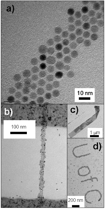
Six arrays were beam-written as single lines and had average widths of 30nm, or four particles across. Two arrays were patterned as slightly wider rectangles, on average seven particles across. Isolated, localized patches where particles formed a second layer made up less than 15% of the area in each of the eight arrays.
All samples were mounted in a shielded cryostat and connected with low-noise coaxial cables to a Keithley 6340 sourcemeter. Temperature was controlled from 8K to 120K, with stability better than 0.1%. We measured the current while ramping the bias voltage between -20V and +20V at rates of 50mV/sec or less. The rms current noise of the set-up was about 10fA.
As a control study, we measured full 2D monolayers before and after e-beam writing and washing. We found that the voltage threshold at a given temperature, and the scaling exponent did not change by more than the fitting uncertainty. This shows that the alkanethiol ligands act as mechanical spacers and, cross-linked or not, do not otherwise influence the properties of the tunneling barrier between the neighboring particles.
III Results and Discussion
Typical current-voltage curves at different temperatures are shown in Fig. 2a. Data from all measured arrays follows power-law scaling, , with voltage thresholds, , in the several-volt regime and scaling exponents, , around two. Figure 2b shows the extent of the power-law scaling. For each temperature, we determined the voltage threshold and the scaling exponent from best straight-line fits on a log-log plot. On closer inspection, Fig. 2a also shows that the shape of the IV traces changes with temperature. This is in contrast to what has been observed for wider, 2D arrays, where the scaling exponent is temperature-independent and the IV curves can be collapsed simply by a translation along the voltage axis. parthasarathyTDep In Fig. 2c, we plot both the extent of the temperature-induced variation in for a given sample and the variation of for different samples. For comparison, we also show the very small variation of the scaling exponent obtained from a series of 2D arrays fabricated with the same Au nanoparticles. parthasarathyIV
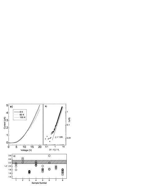
For , on the other hand, we find behavior similar to what has been previously observed in 2D arrays parthasarathyTDep ; boos and in 1D chains, bezryadin namely an approximately linear decrease with increasing temperature. At zero temperature, the voltage threshold can be expressed as , where is the number of particles along the length of the array and corresponds to the typical electrostatic energy cost associated with single electron tunneling between neighboring particles in the array. parthasarathyTDep Because quenched charge disorder leads to a distribution of local energy costs, tunneling will occur along those current paths that minimize penalties and circumvent sites with large local charging energies. The extent to which this happens is measured by the prefactor which depends on the array geometry and dimensionality.
For 2D close-packed arrays, characterized by a large coordination number and thus a multitude of possible detours, theory predicts , while for 1D chains. middleton ; parthasarathyTDep To find experimentally, we obtained directly from TEM images and established by extrapolating the temperature-dependent threshold to zero temperature. Using the procedure described in Ref. elteto, , was calculated from the average radius and center-to-center spacing of the particles in each array, as determined by TEM. Our quasi-1D strips exhibit values between the 1D and 2D theoretical prediction, giving for the eight samples measured.
The observed values for and demonstrate that, even at average widths of only four particles, transport along the arrays has not yet reached the 1D limit. The nonlinear shape of IV curves shows that the current paths are still able to meander and branch significantly, which is the characteristic behavior of 2D transport.
Nevertheless, quasi-1D arrays allow for only a very limited number of parallel paths. We therefore expect that these limited number of current-carrying paths will be inherently more susceptible to changes in the configuration of quenched offset charges in the underlying substrate.

This is borne out by measurements of the fluctuations in the transport current at low temperatures under a fixed bias voltage. We observe clear evidence for random switching between a few well-defined states of the system. The trace at 8K in Fig. 3a shows that the current fluctuates on the order of several minutes between two steady states, which also are easily identified from the histogram in Fig. 3b. The magnitude of the current change in this figure, about 12%, corresponds to one out of four parallel conduction channels in the array changing its transmission by 50%.
As the temperature increases between 8K and 60K, the frequency of this telegraph noise increases and, above 60K, distinct current states can no longer be observed (Fig. 3c). Qualitatively, this change in behavior is expected if the number of active conduction channels in the array depends on the configuration of quenched offset charges in the substrate. With increasing thermal energy, these offset charges can switch more rapidly between different trapping states, inducing the opening and closing of conduction paths. Similar stochastic switching of current was also observed in much wider 2D arrays (with width of ). However, these 2D arrays did not exhibit bimodal switching even at 8K.
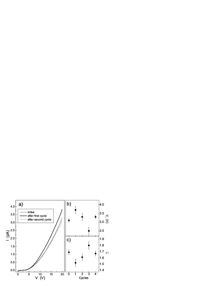
Further evidence that rearrangements of trapped offset charges determine the behavior of the mobile electrons comes from temperature-cycling experiments. In these experiments, we measure the current at 20K, warm up the array to 200K for at least an hour and, and upon cooling back to 20K, measure the current again (Fig. 4a). Such temperature cycles are done several times for the same sample. We find that, in response, the threshold voltage and scaling exponent change randomly (Fig. 4b,c), varying significantly more than the fitting uncertainty given by the error bars. In fact, the changes induced by temperature cycling are of similar magnitude as the sample-to-sample variations (Fig. 2c). This variability contrasts with the robust behavior we find in 2D arrays that are a few hundred particles wide. For 2D arrays, even after temperature cycling, stays within the range indicated in Fig. 2c.
IV Conclusions
In summary, our results demonstrate the important role played by quenched or trapped offset charges in determining the arrays’ overall transport behavior. Being able to control the structural integrity of the arrays down to widths of 4 particles, we conclude that the large variability in threshold voltages and scaling exponents seen in our experiments as well as by others bezryadin ; clarke ; shirley is inherent to the quasi-1D nature of the samples. The fact that there are fewer conduction paths in narrow strips as compared to the extended 2D arrays implies a high sensitivity to the change of the quenched charge disorder “landscape”. This charge reconfiguration is time dependent and induced by thermal activation.
In a 2D array by contrast, changes in the charge configuration and tunneling paths average out, giving a time- and temperature-independent scaling exponent that varies little from array to array. Thus, while quenched charge disorder gives rise to the nonlinear current-voltage characteristics in the first place, quasi-1D structures at any given time sample only a limited range of disorder configurations. This has a significant implication for device applications in which a high degree of reproducibility from sample to sample is desired. In those cases, it will be necessary to use wider nanocrystal arrays in which there is sufficient spatial averaging over different trapped charge disorder configurations.
Acknowledgements.
The authors thank Terry Bigioni and Thu Tran for illuminating discussions, Sang-Kee Eah for sharing the water-drop-depositing technique, and Qiti Guo and Robert Josephs for technical help with the electron microscopes. This work was supported by the UC-ANL Consortium for Nanoscience Research, by the NSF MRSEC program under DMR-0213745, and by the DOE, Basic Energy Sciences-Materials Sciences, under contract #W-31-109-ENG-38.References
- (1) G. M. Whitesides, B. Grzybowski, Science 295, 2418 (2002).
- (2) F. X. Redl, K.-S. Cho, C. B. Murray, S. O’Brien, Nature 423, 968 (2003).
- (3) W. A. Lopes, H. M. Jaeger, Nature 414, 735 (2001).
- (4) J. H. Liao, K. J. Chen, L. N. Xu, C. W. Ge, J. Wang, L. Huang, N. Gu, Appl. Phys. A 76, 541 (2003).
- (5) Yoseph Imry, Introduction to mesoscopic physics (Oxford U. P., Oxford, 2002).
- (6) J. von Delft, D. C. Ralph, Phys. Rep. 345, 61 (2001).
- (7) D. Yu, C. J. Wang, B. L. Wehrenberg, P. Guyot-Sionnest, Phys. Rev. Lett. 92, 216802 (2004).
- (8) N. Y. Morgan, C. A. Leatherdale, M. Drndic, M. V. Jarosz, M. A. Kastner, M. Bawendi, Phys. Rev. B 66, 075339 (2002).
- (9) R. Parthasarathy, X. M. Lin, H. M. Jaeger, Phys. Rev. Lett. 87, 186807 (2001).
- (10) A. A. Middleton, N. S. Wingreen, Phys. Rev. Lett. 71, 3198 (1993).
- (11) C. Reichhardt, C. J. Olson Reichhardt, Phys. Rev. Lett. 90, 046802 (2003).
- (12) R. W. Rendell, M. G. Ancona, IEEE T. Nanotechnol. 2, 75 (2003).
- (13) A. Bezryadin, R. M. Westervelt, M. Tinkham, Appl. Phys. Lett. 74, 2699 (1999).
- (14) L. Clarke, M. N. Wybourne, M. Yan, S. X. Cai, J. F. W. Keana, Appl. Phys. Lett. 71, 617 (1997).
- (15) M. G. Ancona, S. E. Kooi, W. Kruppa, A. W. Snow, E. E. Foos, L. J. Whitman, D. Park, L. Shirey, Nano Lett. 3, 135 (2003).
- (16) R. Parthasarathy, X. M. Lin, K. Elteto, T. F. Rosenbaum, H. M. Jaeger, Phys. Rev. Lett. 92, 076801 (2004).
- (17) X. M. Lin, C. M. Sorensen, K. J. Klabunde, J. Nanopart. Res. 2, 157 (2000).
- (18) X. M. Lin, H. M. Jaeger, C. M. Sorensen, K. J. Klabunde, J. Phys. Chem. B 105, 3353 (2001).
- (19) S. K. Eah, et al. Manuscript in preparation.
- (20) M. H. Werts, M. Lambert, J.-P. Bourgoin, M. Brust, Nano Lett. 2, 43 (2002).
- (21) J. Lohau, S. Friedrichowski, G. Dumpich, E. F. Wassermann, M. Winter, M. T. Reetz, J. Vac. Sci. Technol. B 16, 77 (1998).
- (22) X. M. Lin, R. Parthasarathy, H. M. Jaeger, Appl. Phys. Lett. 78, 1915 (2001).
- (23) M. G. Ancona, W. Kruppa, R. W. Rendell, A. W. Snow, D. Park, J. B. Boos, Phys. Rev. B 64, 033408 (2001).
- (24) K. Elteto, E. G. Antonyan, T. T. Nguyen, H. M. Jaeger, Preprint cond-mat/0407572.