Electrical initialization and manipulation of electron spins
in an L-shaped strained -InGaAs channel
Abstract
An L-shaped strained -InGaAs channel is used to polarize and subsequently rotate electron spins solely by means of electric fields. Precession of electrically-excited spins in the absence of applied magnetic fields is directly observed by Kerr rotation microscopy. In addition, in-plane and out-of-plane components of the spin polarization in the channel are simultaneously imaged.
pacs:
85.75.-d,72.25.Dc,72.25.Pn,71.70.FkSpin-orbit effects offer a unique direction for the development of spintronics Wolf:2001 ; Semiconductor:2002 ; Zutic:2004 by allowing spin-dependent interactions that require neither magnetic fields nor magnetic materials. A number of proposals take advantage of the spin-orbit interaction in semiconductors to construct spintronic devices from nonmagnetic materials, Voskoboynikov:2000 ; Kiselev:2003 ; Ting:2003 ; Hall:2003 ; Governale:2003 and recent experiments have demonstrated various manifestations of the spin-orbit interaction in semiconductor systems. It has been shown that an effective internal magnetic field , which is proportional to the drift velocity of electrons, exists in strained -type GaAs and InGaAs, enabling coherent manipulation of electron spins without magnetic fields. Kato:2004:1 Current-induced spin polarization (CISP) Levitov:1985 ; Edelstein:1990 ; Aronov:1989 has been detected in these systems Kato:2004:2 and in a two-dimensional hole gas at a GaAs/AlGaAs heterojunction, Silov:2004 demonstrating the feasibility of all-electrical spin initialization. The spin Hall effect Dyakonov:1971 ; Murakami:2003 is another phenomenon originating from the spin-orbit interaction and has been observed in -type unstrained GaAs and strained InGaAs, Kato:2004:3 as well as in a two-dimensional hole gas. Wunderlich:2005
Here we show that it is possible to combine CISP and in strained semiconductors to polarize and subsequently rotate electron spins using electric fields alone, without an applied magnetic field. A Kerr microscope images the steady-state spin polarization in an L-shaped channel of strained InGaAs in which the spins orient in one arm and precess in the other arm.
Samples are fabricated from a wafer grown by molecular beam epitaxy on a semi-insulating (001) GaAs substrate (wafer “E” as described in previous works Kato:2004:1 ; Kato:2004:2 ; Kato:2004:3 ), which consists of 500-nm thick -In0.07Ga0.93As (Si-doped for cm-3 to achieve long spin lifetimes Kikkawa:1998 ; Dzhioev:2002 ) capped with 100 nm of undoped GaAs. The InGaAs layer shows anisotropic strain relaxation Kavanagh:1988 but residual strain is present as determined by X-ray diffraction at room temperature. Standard photolithography is employed to define an L-shaped InGaAs channel consisting of two arms, each with a width of 18 m and a length of 200 m, connecting at a right angle [Fig. 1(a)]. The top 0.7 m of the sample is chemically etched to form the mesa, and the two ends of the L-shaped channel are contacted by annealing the following metal layers, Au/Ni/Au/Ge/Ni, listed in order from the surface to the substrate.
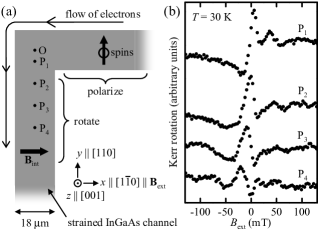
We consider the case where an electric field is applied such that the electrons flow from the horizontal arm to the vertical arm as shown in Fig. 1(a). As the electrons flow to the -direction in the horizontal arm, their spins are polarized in the -direction because of CISP. After the electrons make the right angle turn and start flowing in the -direction down the vertical arm, the electron spins will now see in the -direction and start to precess. This will result in a non-zero component of spin polarization in the -direction, allowing detection by Kerr rotation even at zero external magnetic fields. Previous measurements Kato:2004:1 ; Kato:2004:2 on a sample from the same wafer have shown anisotropy of CISP and for electric field E applied along the two crystal axes and . Larger CISP has been observed when , while is larger for . In order to use this anisotropy to our advantage, we use the axis for the horizontal arm along the -axis and the axis for the vertical arm along the -axis.
Steady-state spin polarization is probed by a low-temperature scanning Kerr microscope in the Voigt geometry. Kato:2004:3 ; Stephens:2003 The sample is placed in a helium flow cryostat, and measurements are performed at a temperature K. A mode-locked Ti:sapphire laser is tuned to a wavelength of 873 nm, and a linearly polarized beam with an average power of 130 W is directed along the -axis (sample growth direction) and focused through an objective lens with a numerical aperture of 0.73 and a working distance of 4.7 mm. The polarization axis of the reflected beam rotates by an amount proportional to the component of net spin polarization along the optical axis (Kerr rotation). A square wave voltage with a frequency = 1.169 kHz is applied to the two contacts and establishes an alternating electric field with an average amplitude . Kerr rotation is detected by a balanced photodiode bridge using a standard lock-in technique. We note that this measurement scheme also detects signal arising from electron flow opposite to that drawn in Fig. 1(a), since the change in the Kerr rotation between positive and negative electric fields is measured.
In Fig. 1(b), Kerr rotation measurements for scans of the external magnetic field applied parallel to the -axis with mV m-1 is shown for various positions on the sample. Although the curves show complex behavior, qualitative explanation is possible with a simple model. We start by considering the steady-state spin polarization prepared in the horizontal channel. As was done in previous work, Kato:2004:2 CISP is modeled as a continuous orientation of spins along the -axis. The -component of the steady-state spin polarization vector just prior to the right-angle turn is
| (1) |
where is the rate of spin orientation onto the -axis, is the inhomogeneous transverse spin lifetime, is the electron Larmor frequency, is the steady-state spin polarization achieved at , is the effective electron g-factor, is the Bohr magneton, and is the Planck constant. Similarly, the -component of the polarization is
| (2) |
which is equivalent to the Hanle curve. Optical:1984
Next, we consider the effect of . If we pick a particular position on the -axis, all spins will display the same precession phase regardless of their drift time since is proportional to the drift velocity of the electrons. Kato:2004:1 Then the -component of spin polarization is
| (3) | |||||
where is the phase that is acquired at the position . We expect , where is the spin-splitting coefficient defined in the previous work, Kato:2004:1 and this relation gives a spatial period of m for this sample. As increases with more negative , the magnetic field dependence deviates from the antisymmetric curve [Fig. 1(b), top curve] to the more symmetric curve [Fig. 1(b), second curve from top]. As the distance from the corner increases, such a model becomes too simplistic. First, since spins do not orient along the -direction after the right-angle turn, the integration limits in Eq. (1) and (2) become less accurate approximations. Second, the spin diffusion transverse to the electric field and the exact trajectory at the corner will affect the line shape. We also note that there are further complications due to the signal from the electron flow in the opposite direction, as mentioned previously. Although CISP in the vertical channel has smaller efficiency Kato:2004:2 and would not precess out of plane since it is parallel to , such a contribution can appear in the vicinity of the corner.
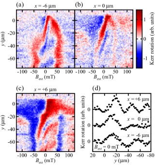
In Fig. 2(a), (b), and (c), Kerr rotation is plotted as a function of and , for m, m, and m, respectively, with mV m-1. Qualitatively, the effect of can be identified in Fig. 2(b), where the main positive peak at mT seen at m shifts to mT as becomes more negative. The electrons that have drifted towards have been affected by so that needs to be applied opposite to to cancel its effect. Line cuts at mT are plotted in Fig. 2(d), showing oscillations as a function of position as expected from the simple sine function obtained by letting in Eq. (3). This result provides unambiguous evidence that is not required for CISP. In the previous work, was used to rotate the polarization in order to allow detection by Kerr rotation, Kato:2004:2 while the data in Fig. 2(d) takes advantage of instead. The oscillation period ranges from 30 to 50 m for the three line cuts. While these values are consistent with the model, the -dependence is currently not understood. In addition to CISP and subsequent precession caused by , we also see the signatures of the spin Hall effect Kato:2004:3 in Fig. 2(a) and (c). For m and around 50 mT, positive peaks are seen in Fig. 2(a) and negative peaks are seen in Fig. 2(c). These peaks can also be seen for m [Fig. 2(b)], although they are much weaker. Such signal contribution from the spin Hall effect can explain some features in individual scans. For example, the small peak at mT in the top curve in Fig. 1(b) is interpreted as arising from the spin Hall effect when the electrons flow from the vertical channel to the horizontal channel, since this peak smoothly shifts into one of the spin Hall peaks for more negative as seen in Fig. 2(b). The spin Hall peak occurring at a smaller can be explained by the reduced -component of electron drift velocity in the vicinity of the corner.
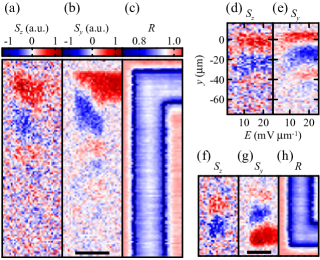
The spatial profile of the spin polarization in the L-shaped channel for mT can be mapped out with a technique previously used to image the spin Hall effect Kato:2004:3 . Here, is sinusoidally modulated at Hz with amplitude of 30 mT, and the signal is detected at and . The former will be proportional to the first derivative of Eq. (3) with respect to and corresponds to at , while the latter is proportional to the second derivative which corresponds to . We show and for mV m-1 in Fig. 3(a) and (b), respectively, and the reflectivity is plotted in Fig. 3(c). The oscillations are clearly resolved, with and being out-of-phase by /2 as expected. The difference in oscillation period for different is reproduced in these images. The contributions from the spin Hall effect do not appear in these images since acts to depolarize spin polarization due to the spin Hall effect when mT. Kato:2004:3
The electric field dependence of the oscillation is investigated by measuring line scans along the -axis at m. In Fig. 3(d) and (e), and are plotted, respectively, as a function of and . The average electron velocity increases with increasing , but the period of oscillations should not change because of the linear relation between and drift velocity. There is no drastic change with as expected, but for small values of , the oscillation period slightly increases. This may be due to diffusion of spins transverse to playing a more important role for small values of , as the above argument only holds for one-dimensional transport of spins.
Finally, we have also fabricated another sample on the same chip, with the vertical channel pointing to (-direction) instead of (-direction). The images for this sample are shown in Fig. 3(f), (g) and (h), and show similar behavior for while the sign of the signal is inverted for . This result is expected as changes sign when the electrons flow direction is changed from to , and this demonstrates the flexibility to control through the shape of the channel. By combining channels with appropriate topology to utilize from different crystal axes, more complicated manipulation of spin states should be possible.
We thank S. A. Wolf for helpful suggestions and acknowledge support from DARPA, DMEA, NSF, and ONR.
References
- (1) S. A. Wolf, D. D. Awschalom, R. A. Buhrman, J. M. Daughton, S. von Molnar, M. L. Roukes, A. Y. Chtchelkanova, and D. M. Treger, Science 294, 1488 (2001).
- (2) Semiconductor Spintronics and Quantum Computation, edited by D. D. Awschalom, D. Loss, and N. Samarth (Springer-Verlag, Berlin, 2002).
- (3) I. Zutic, J. Fabian, and S. Das Sarma, Rev. Mod. Phys. 76, 323 (2004).
- (4) A. Voskoboynikov, S. S. Lin, C. P. Lee, and O. Tretyak, J. Appl. Phys. 87, 387 (2000).
- (5) A. A. Kiselev and K. W. Kim, J. Appl. Phys. 94, 4001 (2003).
- (6) D. Z. Y. Ting and X. Cartoixa, Appl. Phys. Lett. 83, 1391 (2003).
- (7) K. C. Hall, W. H. Lau, K. Gundogdu, and M. E. Flatte, Appl. Phys. Lett. 83, 2937 (2003).
- (8) M. Governale, F. Taddei, and R. Fazio, Phys. Rev. B 68, 155324 (2003).
- (9) Y. Kato, R. C. Myers, A. C. Gossard, and D. D. Awschalom, Nature 427, 50 (2004).
- (10) L. S. Levitov, Y. V. Nazarov, and G. M. Eliashberg, Sov. Phys. JETP 61, 133 (1985).
- (11) V. M. Edelstein, Solid State Commun. 73, 233 (1990).
- (12) A. G. Aronov and Y. B. Lyanda-Geller, JETP Lett. 50, 431 (1989).
- (13) Y. K. Kato, R. C. Myers, A. C. Gossard, and D. D. Awschalom, Phys. Rev. Lett. 93, 176601 (2004).
- (14) A. Y. Silov, P. A. Blajnov, J. H. Wolter, R. Hey, K. H. Ploog, and N. S. Averkiev, Appl. Phys. Lett. 85, 5929 (2004).
- (15) M. I. Dyakonov and V. I. Perel, JETP Lett. 13, 467 (1971).
- (16) S. Murakami, N. Nagaosa, and S. C. Zhang, Science 301, 1348 (2003).
- (17) Y. K. Kato, R. C. Myers, A. C. Gossard, and D. D. Awschalom, Science 306, 1910 (2004).
- (18) J. Wunderlich, B. Kastner, J. Sinova, and T. Jungwirth, Phys. Rev. Lett. 94, 047204 (2005).
- (19) J. M. Kikkawa and D. D. Awschalom, Phys. Rev. Lett. 80, 4313 (1998).
- (20) R. I. Dzhioev, K. V. Kavokin, V. L. Korenev, M. V. Lazarev, B. Y. Meltser, M. N. Stepanova, B. P. Zakharchenya, D. Gammon, and D. S. Katzer, Phys. Rev. B 66, 245204 (2002).
- (21) K. L. Kavanagh, M. A. Capano, L. W. Hobbs, J. C. Barbour, P. M. J. Maree, W. Schaff, J. W. Mayer, D. Pettit, J. M. Woodall, J. A. Stroscio, and R. M. Feenstra, J. Appl. Phys. 64, 4843 (1988).
- (22) J. Stephens, R. K. Kawakami, J. Berezovsky, M. Hanson, D. P. Shepherd, A. C. Gossard, and D. D. Awschalom, Phys. Rev. B 68, 041307(R) (2003).
- (23) Optical Orientation, edited by F. Meier and B. P. Zakharchenya (Elsevier, Amsterdam, 1984).