Permanent address: ]Institute of Molecular Physics, P.A.S., Smoluchowskiego 17, 60-179 Poznań, Poland
Spin accumulation and decay in magnetic Schottky barriers
Abstract
The theory of charge and spin transport in forward-biased Schottky barriers reveals characteristic and experimentally relevant features. The conductance mismatch is found to enhance the current induced spin-imbalance in the semiconductor. The GaAsMnAs interface resistance is obtained from an analysis of the magnetic field dependent Kerr rotation experiments by Stephens et al. and compared with first-principles calculations for intrinsic interfaces. With increasing current bias, the interface transparency grows towards the theoretical values, reflecting increasingly efficient Schottky barrier screening.
pacs:
72.25.Hg, 72.25.Mk, 73.30.+y,78.47.+pAn obstacle to the direct injection of spins from a ferromagnetic metal (F) into a semiconductor (SC) is the so-called conductance mismatch Schmidt00 . Paradoxically, this problem is most severe for good electric contact, because most of the applied potential drop is then wasted over the highly resistive semiconductor and very little is left to spin-polarize the current in the magnetically active region. Selection rules at ballistic interfaces are responsible for a large interface spin polarization Wunnicke ; Zwierzycki that allows significant spin accumulation in spite of the mismatch, but even small amounts of disorder have detrimental effects Zwierzycki . Use of ferromagnets with low conductances matched to those of the semiconductor Fiederling99 is another route, but many material problems, such as low critical temperatures for ferromagnetism, have still to be solved Ohno . Spins can be effectively injected into a semiconducting base contact of a three-terminal spin-flip transistor Brataas00 or by pumping spins into the semiconductor by ferromagnetic resonance Brataasb , but none of these theoretical predictions have been confirmed experimentally yet. The spin polarization of the injected current can be increased by tunneling or Schottky barriers, both causing the applied potential to drop in the spin-selective region of the sample Schmidt00 ; Rashba00 ; Fert01 . This feature has been employed in experiments that divide into two categories. In the first, hot electrons are injected into a metallic magnetic multilayer base in the forward bias regime. In the “spin-valve transistor” Monsma this is achieved via a Schottky barrier; in “magnetic tunnel transistors”, tunneling barriers are used instead Parkin . The second category of experiments concentrates on injecting spins from the ferromagnet into semiconductors by applying a reverse bias, reaching polarizations of 30 % Jonker . Here the spin current is the observable, measured by the circular polarization of the recombination luminescence of the injected electrons with thermalized holes.
Recently, Stephens et al. Stephens investigated in forward-biased Schottky barriers not the hot electrons that traverse a ferromagnetic base as in Refs. Monsma ; Parkin , but the cold ones that remain in the semiconductor. A significant bias-dependent spin accumulation in the semiconductor was observed by Kerr rotation. The interpretation as spin dependent reflection at the interface was supported by a simple parabolic band/step potential model. In this Letter we present a theoretical analysis based upon an adaptation of magnetoelectronic circuit theory Brataas00 ; Bauer04 . We find that the conductance mismatch has a beneficial effect on the size of the spin accumulation. Analyzing the Bloch equation that governs the spin accumulation in the presence of an applied magnetic field we find that the experimental results on the dephasing by a magnetic field (Hanle effect) can be used to extract the SCF interface resistance. We also present first-principle calculations of intrinsic interface transport parameters for disordered interfaces as a function of the SC Fermi energy.
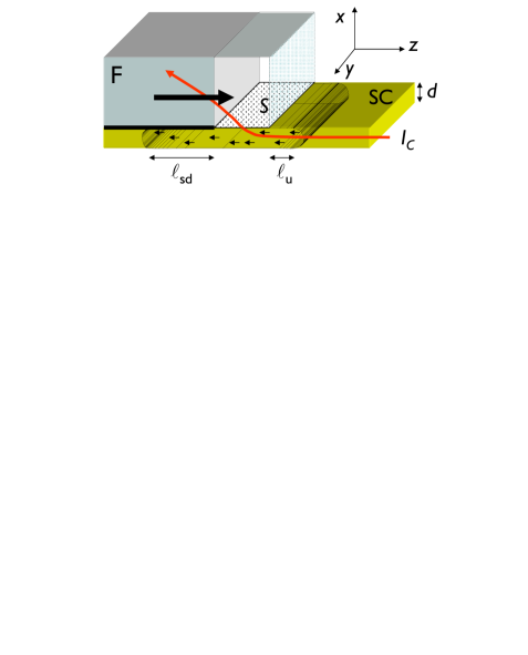
The sample configuration is indicated in Fig. 1. We start with a discussion of an infinite planar Schottky barrier model between a degenerately n-doped semiconductor SC and a metallic ferromagnet F that is kept at low temperatures and biased with an electric particle current . With increasing forward (positive) bias the semiconductor band edge is lifted relative to the ferromagnetic one. The ionized donor atoms are increasingly screened until at a bias close to the Schottky barrier height the semiconductor band edge at the interface comes close to the bulk Fermi energy of the semiconductor . The “flat-band” condition is defined asymptotically at a voltage close to the barrier height where the tunneling current and thus the electric field in the semiconductor start to become significant. Although the theory is valid for arbitrary material combinations we concentrate here on the sample investigated by Stephens et al., in which the GaAs is n-doped with densities of . With an impurity scattering mean free path of the semiconductor is safely in the diffuse transport regime. The I-V characteristic in the forward bias shows a band tail close to the Schottky barrier and roughly Ohmic behavior at high bias with a resistance of 300 , indicating that the thin semiconductor layer limits the transport. Important parameters are the spin-flip diffusion length of Kikkawa , and a flat-band depletion length of . Any residual band-bending is thus incorporated in the (quantum) interface resistance. The conductance of the high-density metallic ferromagnet MnAs is much higher than that of the semiconductor and disregarded. We concentrate on the dimensionless spin-dependent occupation function in the semiconductor near the interface at an energy from the band edge. The up spin direction is chosen parallel to the majority spin in the ferromagnet. Close to the flat band condition the energy of the electrons entering the metal is of the order of the Schottky barrier height, that is much larger than the semiconductor Fermi energy. The spectral spin current into the metal is therefore
| (1) |
where is the interface conductance at energy . The total current of spin is given integrating over energy
| (2) |
We assume a charge current bias of and introduce the spin current We assume in the following that energy relaxation is fast, such that the distribution function at the interface is thermalized with non-equilibrium chemical potentials . At low temperatures, assuming local charge neutrality and an interface conductance that does not vary rapidly on the scale of :
| (3) | ||||
| (4) |
| (5) |
where is the spin accumulation at the interface and
| (6) |
In the degenerate limit, assuming that the conductivity is proportional to the density, the magnetically active region of the semiconductor is determined by the up-stream spin-diffusion length , where is a measure of the potential drop induced by the current over the (zero-bias) spin diffusion length in terms of the linear bulk conductance of a semiconductor cube with area and thickness Flatte . In spite of the reduced spin-diffusion length, the conductance of the spin-coherent region is increased compared to the zero-bias limit:
| (7) |
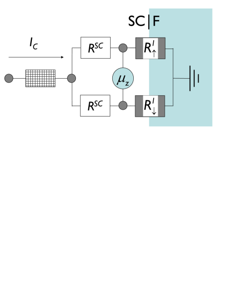
(not as might be expected naively). We then arrive at the effective circuit in Fig. 2, according to which the spin current that flows from the semiconductor bulk to the interface reads
| (8) |
and the sign of is opposite to that of . A low conductance suppresses the spin current Schmidt00 , but not the spin accumulation! By reversing and keeping in mind that the interface conductance is in general much smaller and less bias dependent, similar equations hold as well for reversed-bias Schottky barriers. As mentioned above, most experiments on reverse bias junctions focus on the spin current. The conductance mismatch problem is reflected in Eq. , where a small semiconductor conductance is seen to suppress the spin current. In Refs. Schmidt00 ; Fert01 it was pointed out that a significantly polarized spin current can only be achieved when the reverse-bias Schottky barrier conductance is sufficiently small. However, in this case the spin accumulation is suppressed, which explains why Stephens et al. Stephens only detected spin accumulation with a forward bias.
We now turn to the spin-accumulation in the presence of a variable in-plane magnetic field, taking the magnetization of F to be parallel to the direction and the magnetic field in the direction. The magnetic-field induced non-collinearity of spin accumulation and magnetization creates a spin transfer torque on the ferromagnet, thus opens new decay channels Bauer04 proportional to the spin-mixing conductance at the Fermi energy Brataas00 . The Bloch equation for the spin accumulation can be written
| (9) |
where is the interface relaxation time in terms of the (single spin) semiconductor energy density of states in the magnetically active volume.
| (10) |
where and the Larmor frequency in terms of the g-factor and the Bohr magneton Eq. (9) holds when the relaxation rate of the electron orbital degrees of freedom is sufficiently larger than . The source term is the current bias applied to the semiconductor. The stationary state solution for the Bloch equation, is easily obtained analytically. The spin accumulation at the interface reads:
| (11) |
Stephens et al. Stephens found the component of the spin accumulation normal to the interface well represented by a Lorentzian . This form also follows from our rate equations with
| (12) |
and In the limit of a highly resistive semiconductor, , and taking , we find that and i.e. the zero field spin accumulation. It is therefore possible to obtain information about the interface conductance from the experimental spin dephasing time.
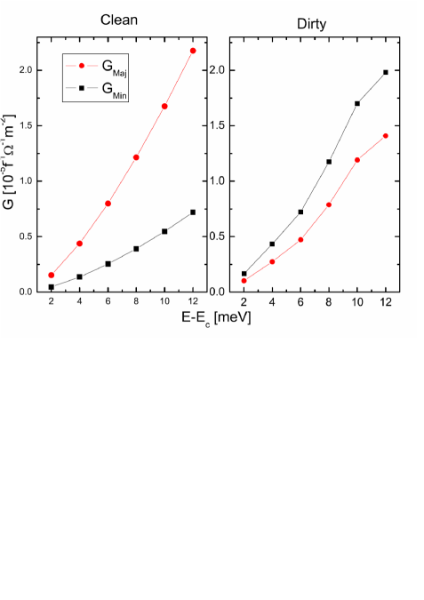
The MnAsGaAs systems has been studied intensively Tanaka , but not much is known about the electronic transport properties. Epstein et al. Epstein1 reported that the conductance polarization is opposite to the magnetization direction, i.e. . We compute MnAsGaAs (100) interface conductances for the ZincBlende structurebeta by scattering matrix calculations with a first-principles tight-binding basis Zwierzycki , assuming flat-band conditions with a Schottky barrier height of 0.8 eV (see Fig. 3). We find large differences between clean, and on a monolayer scale, alloy-disordered interfaces, e.g. the interface polarization changes sign when the interface becomes increasingly dirty. The negative polarization found in Epstein1 is thus consistent with non-ideal interfaces. These features are quite similar to results for FeInAs that does not have a Schottky barrier Zwierzycki . We also note that in the regime considered here we calculate an in all cases and for clean (disordered) interfaces. We parametrize the estimated interface conductance in terms of the SC Sharvin conductance times a transparency parameter that at 12 meV is found to be for clean and dirty interfaces.
In order to make contact with Stephens et al. Stephens the above results for the planar junction have to be adapted to the experimental geometry in Fig. 1. For GaAs with doping density we take a mobility 3000 cm, an effective mass and spin-flip diffusion length Kikkawa , that is significantly larger than the film thickness . The measured excess spin-dephasing rates at applied currents are listed in the table. Close to the interface, the up-stream spin-flip diffusion length is not significantly reduced, so not only the whole area under the conducting contact is spin coherent at all currents, but also strips on both sides with widths of the order of and , respectively. The drift effect on the available density of states is small, but it significantly affects the resistance of the spin coherent region. Due to the thin layer thickness of the GaAs, lateral spin diffusion may be disregarded. The results in the table are obtained assuming that
The experimental longevity of spins is striking and can only be explained by a reduced interface conductance. Any spin-flip process disregarded here, caused, e.g., by heating Kikkawa due to high currents, would correspond to even smaller transparencies. The small at small bias reflects the residual Schottky barrier that is not yet completely screened. At higher bias these remnants should disappear and the spin-dephasing time should be governed by the intrinsic interface. At higher bias the interface conductances deduced from the experiments grow to about one third of the intrinsic first-principles results. An energy-averaged interface transparency is accessed by the electrical current itself. Disregarding the small term proportional to in Eq. (5), the current according to the first-principles conductances and a contact area of should be . At the experimental currents of the average is thus smaller than that at the Fermi energy obtained from the Hanle effect. This can be explained by an energy dependent that decreases strongly when approaching the band edge. These remaining puzzles might be related to the measured Stephens spatial inhomogeneity of the current induced spin accumulation and thus interface conductance.
Stephens et al. Stephens estimate the spin accumulation to be 10% of the Fermi energy from nuclear polarization data compared to an estimate of 15% based on the first-principles results for disordered interfaces. The spin accumulation is found to saturate and even decrease again with large A probable reason is a reduced spin-flip diffusion length, either by heating or by a large drift contribution at higher bias.
In summary, we demonstrate how a transport property, the semiconductorferromagnet interface conductance, can be measured optically on an absolute scale. The conductance mismatch is found to favor spin injection into semiconductors in forward-biased magnetic Schottky barriers. At low bias the interface-mediated spin-decay is much weaker in the experiments Stephens than expected from intrinsic SCF interfaces. At higher bias the agreement becomes better, indicating that the interface approaches (but does not reach) the Ohmic limit as calculated from first-principles. Experiments that determine the spin accumulation on an absolute scale would be of great help to refine the present analysis. The observed negative polarization Epstein1 ; Stephens can be explained by disorder at the interfaces. A systematic study as a function of semiconductor thickness could shed more light on the spin-decoherence in the non-linear transport regime.
We thank Georg Schmidt, David Awschalom, and Jason Stephens for helpful discussions. This work has been supported by the FOM Foundation and the EU Commission FP6 NMP-3 project 505587-1 “SFINX”.
References
- (1) G. Schmidt, D. Ferrand, and L. W. Molenkamp, A. T. Filip, and B. J. van Wees, Phys. Rev. B 62, 4790 (2000).
- (2) O. Wunnicke, Ph. Mavropoulos, R. Zeller, P.H.Dederichs, and D. Grundler, Phys. Rev. B 65, 241306 (2002).
- (3) M. Zwierzycki, K. Xia, P. J. Kelly, G.E.W. Bauer, and I. Turek, Phys. Rev. B 67, 092401 (2003).
- (4) R. Fiederling, M. Keim, G. Reuscher, W. Ossau, G. Schmidt, A. Waag, and L. W. Molenkamp, Nature 402, 787 (1999); Y. Ohno, D. K. Young, B. Beschoten, F. Matsukura, H. Ohno, and D. D. Awschalom, Nature 402, 790 (1999).
- (5) H. Ohno, Institute of Physics Conference Series 171, 37 (2003).
- (6) A. Brataas, Yu.V. Nazarov, and G.E.W. Bauer, Phys. Rev. Lett. 84, 2481 (2000); Eur. Phys. J. B 22, 99 (2001).
- (7) A. Brataas, Y. Tserkovnyak, G.E.W. Bauer, and B.I. Halperin, Phys. Rev. B 66, 060404 (2002).
- (8) E. I. Rashba, Phys. Rev. B 62, R16267 (2000).
- (9) A. Fert and H. Jaffres, Phys. Rev. B 64, 184420 (2001).
- (10) D.J. Monsma, J.C. Lodder, Th.J.A. Popma, and B. Dieny, Phys. Rev. Lett. 74, 5260 (1995); O. M. J. van’t Erve, R. Vlutters, P. S. Anil Kumar, S. D. Kim, F. M.Postma, R. Jansen, and J. C. Lodder, Appl. Phys. Lett. 80, 3787 (2002).
- (11) S. van Dijken, X. Jiang. and S.P. Parkin, Appl. Phys. Lett. 83, 951 (2003); I. Appelbaum, K. J. Russell, D. J. Monsma, V. Narayanamurti, C. M. Marcus, M. P. Hanson, and A. C. Gossard; Appl. Phys. Lett. 83, 4571 (2003)
- (12) O.M.J. van ’t Erve, G. Kioseoglu, A.T. Hanbicki, C.H. Li, and B.T. Jonker, R. Mallory, M. Yasar, and A. Petrou, Appl. Phys. Lett. 84, 4334 (2004) and references therein.
- (13) J. Stephens, J. Berezovsky, J. P. McGuire, L. J. Sham, A. C. Gossard, and D. D. Awschalom, Phys. Rev. Lett 93, 097602 (2004).
- (14) G.E.W. Bauer, A. Brataas, Y. Tserkovnyak, B. I. Halperin, M. Zwierzycki, and P. J. Kelly, Phys. Rev. Lett. 92, 126601 (2004); M. Zaffalon and B.J. van Wees, cond-mat/0411407.
- (15) M. Tanaka, Sem. Sc. Techn. 17, 327 (2002).
- (16) J. M. Kikkawa and D. D. Awschalom, Phys. Rev. Lett. 80, 4313 (1998).
- (17) Z. G. Yu and M. E. Flatté, Phys. Rev. B 66, 235302 (2002).
- (18) R.J. Epstein, I. Malajovich, R.K. Kawakami, Y. Chye, M. Hanson, P.M. Petroff, A.C. Gossard, and D.D. Awschalom, Phys. Rev. B 65, 121202 (2002).
- (19) Preliminary results on geometry optimized -MnAsGaAs interface show interesting differences, such as a negative polarization for specular interfaces and a stronger dependence of on disorder morphology (P.-X. Xu, J. Ren, K. Xia et al., unpublished).