New Type of Fano Resonant Tunneling via Anderson Impurities in Superlattice
Abstract
The spectrum of differential tunneling conductance in Si-doped GaAs/AlAs superlattice is measured at low electric fields. The conductance spectra feature a zero-bias peak and a low-bias dip at low temperatures. By taking into account the quantum interference between tunneling paths via superlattice miniband and via Coulomb blockade levels of impurities, we theoretically show that such a peak-dip structure is attributed to a Fano resonance where the peak always appears at the zero bias and the line shape is essentially described by a new function with the asymmetry parameter . As the temperature increases, the peak-dip structure fades out due to thermal fluctuations. Good agreement between experiment and theory enables us to distinguish the zero-bias resonance from the usual Kondo resonance.
pacs:
72.10.Fk,73.21.Cd,73.23.HkThe Fano effect c1 ; fano is a consequence of interference between a localized state and a continuum that results in an asymmetric line shape of the resonance created by this localized state. The necessary conditions for the observation of the Fano line shape in a resonance are the coexistence of the localized state and the continuum, and the quantum coherence between two transition paths. In condensed-matter physics, the Fano effect was observed in a wide variety of spectroscopy, such as atomic photoionization, c2 optical absorption,c3 Raman scattering,c4 scanning tunneling through a surface impurity atom,c5 ; c6 and phonon-assisted photoluminescence.xu Owing to the progress in fabrications of nanodevices, the system sizes become comparable with the coherence length and hence the Fano resonance has also been observed in the transport through mesoscopic systems containing quantum dots c7 ; marcus ; c8 and carbon nanotubes.c9 ; xie Moreover, it is proposed that the Fano resonance can be used as a probe of the phase coherence in the transport of electrons or other quasiparticles.c10 ; c11 On the other hand, electric-field induced Stark localization,bastard ; mendez negative differential conductance,sibble and Fano resonance due to quantum interference between Stark levelsleo have been reported in semiconductor superlattices with wide minibands. In this Letter, we report an observation of new type of Fano resonance in perpendicular tunneling of electrons through Si-doped GaAs/AlAs superlattice with 30 periods. The spectrum of differential conductance at low electric fields shows a clear zero-bias resonance and a low-bias dip at low temperatures. Simply increasing the temperature can lead to weakening of such a peak-dip structure, revealing the coherence nature of the resonance. From the energy structure of the system, there are two tunneling paths for electrons: the many-body states of Si impurities and the superlattice lowest miniband. Although the hydrogen-like donor levels are below the bottom of the miniband and have no contribution to the Fano resonance, the double-occupation levels of these states are above the Fermi energy due to the Coulomb blockade effect and can serve as the localized states in the Fano effect. Starting from this picture we are able to analytically derive a new line shape function to describe the observed peak-dip feature where the peak is proved to be always at the zero bias independent of parameter values and to spread out with increasing temperature. We also discuss the difference of this zero-bias peak from the usual Kondo resonance.
The sample used in the experiment is a GaAs/AlAs superlattice grown by molecular beam epitaxy on a -type GaAs substrate. The structure consists of 30 periods of 14 nm GaAs well and 2.5 nm AlAs barrier. The central 10 nm region of each well is Si doped (4 1017 cm-3). The key of the designing is in the precise adjustment of the Si doping density and Al concentration of the bottom and top AlGaAs contact layers to eliminate the possible built-in electric field. We minimize the misalignment between the Fermi levels in the doped superlattice and both contact layers in the absence of the bias. Standard semiconductor fabrication processes were employed to fabricate the sample into the -- mesa diodes with an area of 200 m 200 m.
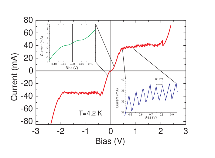
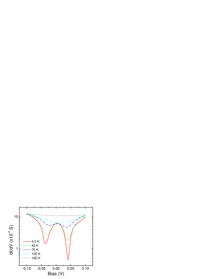
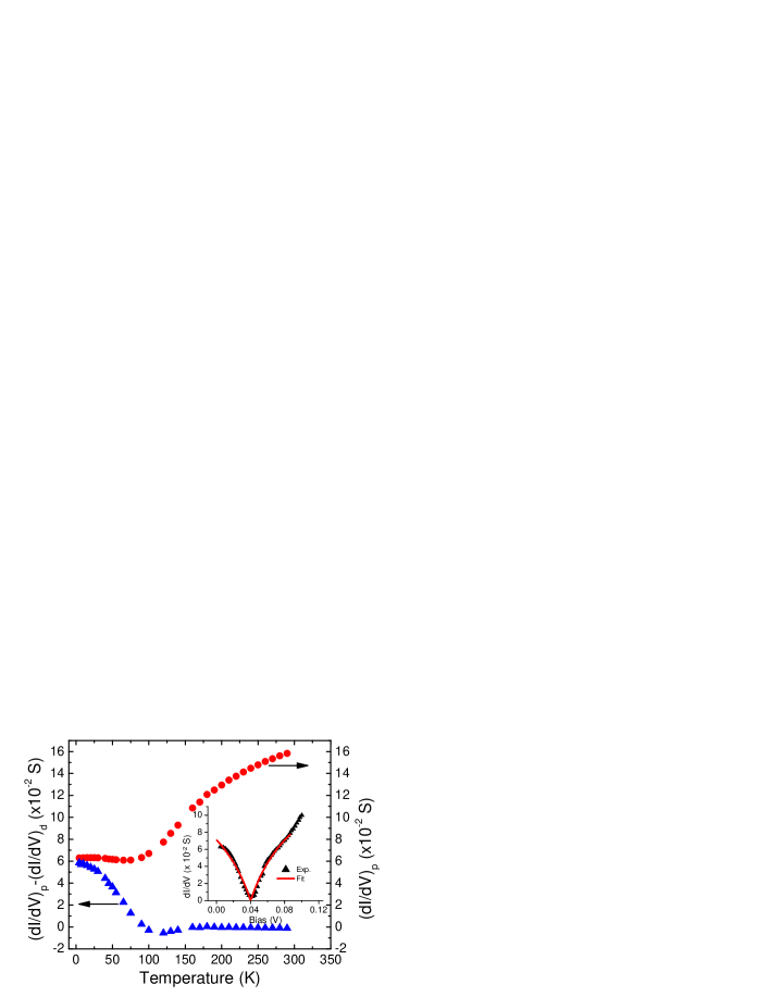
Figure 1 shows the current-voltage curves of the sample measured at 4.2 K. Two distinct transport characteristics, as shown in the inset figures, can be identified. In the high-field region, the saw-like current oscillations with a period of 60 mV appear due to the well-known sequential resonance tunneling, also called high-field domain effect.13 ; 14 The characteristic in the low-field region is our main interest in the present work. Firstly, the linear - relation within a bias region from about -10 mV to about 10 mV indicates a finite differential conductance () at zero bias. Secondly, the current exhibits a saturation in a range about 40 mV bias, corresponding to a dip in at an average potential drop of 1.3 meV across a barrier-well supercell. The semilogarithmic differential conductance of the sample as a function of the bias voltage is plotted in Fig. 2 for various temperatures. A peak near the zero bias is clearly seen at low temperatures. In accordance to the current saturation shown in Fig. 1, the differential conductance exhibits two minima (dips) at the bias voltage of mV. In spite of slight asymmetry probably due to small difference in Fermi level between the bottom and top contact layers, both dips, especially the dip at +40 mV, are close to zero at 4 K. Furthermore, the dips gradually disappear as temperature increases beyond 100 K. As mentioned earlier, in each well of the superlattice there exist hydrogen-like orbits at Si donors and a continuum of two-dimensional (2D) electron states. Although the levels of hydrogen-like orbits themselves are below the miniband bottom and have no contribution to the inter-well tunneling, the levels of double occupation on them should go up due to the Coulomb blockade (CB) effect and are near the Fermi level. Thus, there are two types of inter-well tunneling paths, one via the CB levels of Si donors and the other via the superlattice miniband. Naturally, we can attribute the zero bias peak to the constructive Fano interference between paths via the CB levels and via the miniband. At the same time, the dips in differential conductance are originated from the destructive Fano interference. In Fig. 3 we display the temperature dependence of the zero-bias differential conductance which shows an interesting temperature dependence. We also depicts the difference in the differential conductances between the peak and the dip as a function of temperature. The difference drops with increasing temperature as a result of thermal fluctuations. The inset in Fig. 3 shows the line shape fitting curve using the new function derived later. The experimental spectrum can be fitted very well.
The basic features of low-bias behavior shown in Figs. 1 and 2 are: (1) At low temperatures there is a peak at the zero bias and a cuspidal dip at a finite bias in curves of differential conductance versus bias voltage; (2) The peak-dip structure is gradually smoothed by increasing the temperature. Theoretically, the transport in such systems could be attributed to impurity assisted tunneling or to Kondo resonant tunneling. However, the mechanism of impurity assisted tunneling usually gives peaks at finite bias and can not explain the dip structure.aaa On the other hand, although the Kondo effect can provide a peak at the zero bias, the peak width and the temperature are too snall, inconsistent with the observed results. Furthermore, in the system many impurities are involved, this makes the zero-bias peak become much narrower.bbb We now turn to a new theoretical analysis for this observed peak-dip structure. The motion of electrons in the perpendicular direction of the superlattice at low bias is related to the minibinds which are formed by the coupling between 2D electron continuum in adjacent quantum wells. The energy of an electron within a quantum well can be written as
| (1) |
where is the dimensionless wave vector in the parallel plane, is the quantized energy in the perpendicular direction with being the level index, and is the hopping energy describing the in-plane motion in the tight-binding representation. can be estimated by with being the effective mass and the lattice spacing. In the wells ,18 with the free electron mass. On the other hand, the Si atoms doped in the middle region of each well become hydrogen-like centers with positive charge after contributing electrons. Because the wells are wide enough ( Å), we can neglect the effect of the well structure on the hydrogen-like states, which are bound to silicon impurities with a binding energy -7 meV and a radius of 88 Å estimated from the effective mass and a dielectric constant . The Coulomb repulsion energy for double occupation is estimated from the size to be meV. Thus, for a quantum well one has a schematic energy spectrum illustrated by the density of states in Fig. 4. The electrons are donated by Si impurities in the wells and in the contact layers. They fill up the hydrogen-like orbits and the lowest 2D continuum to form a Fermi level . Thus, is usually between the bottom of the 2D continuum and the double occupation level, but its precise position is influenced by other physical ingredients such as the bend of the potential and the doping in contact layers.

By introducing the inter-well tunneling in superlattice, the quantized energy in isolated wells is extended to a miniband as one of the major transport paths in the perpendicular direction. Due to the existence of the Si impurities and inevitable roughness at interfaces, the parallel momenta are not necessarily conserved in the inter-well tunneling. On the other hand, the widths of wells and barriers in the superlattice make the lowest superlattice miniband in the perpendicular direction certainly narrow (only 0.3 meV as calculated from the Kronig-Penny model of superlattice potential profile). Thus, at low temperatures and low but finite bias (larger than the order of meV), the miniband tunneling is based on the resonance in the perpendicular direction but without strict matching of parallel momenta between the adjacent wells. In fact, when an electron is tunneling from one well to a sequent well due to a bias between them, the kinetic energy in the perpendicular direction should be kept almost the same so that the sharp resonance maintains, and the energy gained from the bias should be transferred to the kinetic energy in the parallel direction. This kind of energy transfer can take place due to elastic scattering from the interface roughness or impurities which makes inter-well tunneling between different parallel momenta possible. On the contrary, the contribution from the completely coherent tunneling with conservation of parallel momenta is vanishingly small owing to the narrow miniband width in the perpendicular direction smaller than the inter-well bias. Since the parallel momenta are not fixed, the tunneling spectrum is determined by the density of states of wells near the Fermi level, rather than by the miniband structure in the perpendicular direction. As can be seen from Fig. 4, the spectral density in a well near the Fermi surface is certainly flat, giving only structure-less tunneling spectrum. So the observed peak-dip structure in differential conductance at low bias is a more distinct effect, suggesting a specific interfering mechanism. Actually, besides the miniband transport discussed above, there is another path for perpendicular motion of electrons, i.e., the path via the hydrogen-like states of Si atoms. In the present case the latter is related to the Coulomb blockade levels of these states.
Below we use a tight-binding chain with sites at centers of barriers to describe the perpendicular motion in the miniband. The site spacing is defined as the size of a supercell, and the hopping between adjacent sites in the chain is associated with the miniband width. In this tight-binding representation, model Hamiltonian for the perpendicular motion through a supercell can be written as:
| (2) |
where and denote the states in two ends of the supercell, and are creation operators of electrons in state and in the th hydrogen-like orbit, respectively, and is the hopping between state at the th end of the well and the hydrogen-like orbit . Note that in the Hamiltonian the strict conservation of the parallel momentum is not necessary for the perpendicular resonant transport. As mentioned above, the resonant tunneling within the narrow miniband in the perpendicular direction is kept. Thus, when an electron is injected from one end of the supercell under a bias , its wave function can be expressed by a superposition
| (3) |
where and are amplitudes of reflected and transmitted waves, is the parallel part of wave function with the parallel kinetic energy within a small bin at , is the position of the th site in the chain, is the wave vector in the perpendicular direction, and is the amplitude on impurity . By applying the Hamiltonian on , we obtain the following equations:
| (4) |
| (5) |
| (6) |
where is the energy of electron, and with being the number of 2D states in the energy bin. Here, we omit the spin index as electrons with up and down spins have the same probability to tunnel through two paths if there is no spin polarization in impurities. The kinetic energy in parallel directions does not appear in the equations since it is restricted by energy and perpendicular wave vector . Because the distribution of Si impurities is symmetric about the center of the well, it is reasonable to assume that the average hopping from Si impurities to both ends is symmetric, namely, . Solving Eqs. (4), (5), and (6) yields the transmission coefficient as
| (7) |
Since the bias applied to the superlattice is much larger than the width of superlattice miniband, it can be assumed that the entire miniband is within the energy window spanned by the bias. So the inter-well transmission is determined by the whole miniband and the averaging over all has to be done. After performing this average, we have
| (8) |
The peak-dip structure in appears when , otherwise it is only a constant. From the transmission coefficient one can calculate the tunneling current through a supercell with the Landauer formula
| (9) |
where is related to the in-plane area of the system and
is the Fermi-Dirac statistical distribution. One has the bias-dependent differential conductance
| (10) |
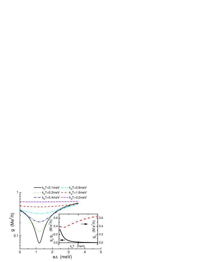
By taking values of parameters , , , and estimated above, we calculate the bias and temperature dependence of differential conductance and show the results in Fig. 5. It is interesting to note that the peak-dip structure is well reproduced at low temperatures. By increasing the temperature, the peak-dip structure is rapidly removed. The characteristic temperature for this transition is in the order of several tens of Kelvin. This is also in agreement with the experiment.
From Eqs. (8) and (10), at low temperatures one has the following function to describe the asymmetric line shape in bias dependence of differential conductance
| (11) |
where is the renormalized bias:
Although the above formulas are derived for one supercell, the same results can be obtained for other supercells because each of them has the same drop of the Fermi energy providing the same energy window for the tunneling electrons. This ensures the same current in any parts of the chain. It is interesting to note that the line-shape function of Eq. (11) is different from the standard Fano line shape function . Especially, from Eq. (11) the peak is always at the zero bias () as long as . Although this zero-bias peak seems like the Kondo resonance, it is much wider, and is more robust against temperature. So the Kondo effect could be excluded from the possible mechanisms for the observed zero-bias peak.
It should be emphasized that the miniband transport here is different from that in short-period superlattices with much wider miniband, e.g., 30 meV or larger.sibble In the latter the miniband transport is based on the coherent inter-well tunneling with conserved parallel momentum manifested by the negative differential conductance sibble or the Wannier-Stark localization mendez under an electric field. In the present case the miniband is extremely narrow so that the effective inter-well tunneling originates only from processes without conservation of parallel momentum. Interfering with the tunneling paths via the Coulomb blockade levels of Anderson impurities, the transport paths provided by the narrow miniband as a whole result in the observed special Fano resonance with line shape described by function of Eq. (11).
In conclusion, we have measured conductance of silicon doped GaAs/AlAs superlattice along the direction perpendicular to the layers. The differential conductance shows a zero-bias peak accompanied with nearby dips at low temperatures. These features suggest that the Fano interference between miniband transport and transport via hydrogen-like orbits on Si impurities dominates the electron transport at low temperatures and at low electric-fields. The observed peak-dip structure and its temperature dependence can be well reproduced by calculations of differential conductance on basis of quantum interference of two transmission channels.
Acknowledgments: Main experimental work was carried out at State Key Laboratory for Superlattices and Microstructures, Institute of Semiconductors, Beijing. We wish to thank H. Guo, T. K. Ng, and X. C. Xie for valuable discussions. The authors gratefully acknowledge X. P. Yang and P. H. Zhang for the growth of the sample, C. F. Li for processing the sample, and Y. X. Li for her contribution in the measurements of the low-temperature - relation and of conductance spectra. S-JX wishes to thank research support from Chinese National Foundation of Nature Sciences (Nos. 60276005 and 10474033). H. Z. Zheng wishes to thank the supports from Major State Basic Research Project (No. G001CB3095), Special Project from Chinese Academy of Sciences.
References
- (1) U. Fano, Phys. Rev. 124, 1866 (1961).
- (2) U. Fano and J. W. Cooper, Phys. Rev. 137, A1364 (1965); Rev. Mod. Phys. 40, 441 (1968).
- (3) U. Fano and A. R. P. Rau, Atomic Collision and Spectra, (Academic Press, Orlando, 1986).
- (4) J. Faist, F. Capasso, C. Sirtori, K. W. West, and L. N. Pfeiffer, Nature (London) 390, 589 (1997).
- (5) F. Cerdeira, T. A. Fjeldly, and M. Cardona, Phys. Rev. B 8, 4734 (1973).
- (6) V. Madhavan, W. Chen, T. Jamneala, M. F. Crommie, and N. S. Wingreen, Science 280, 567 (1998).
- (7) J. Li, W.-D. Schneider, R. Berndt, and B. Delley, Phys. Rev. Lett. 80, 2893 (1998).
- (8) S. J. Xu, S.-J. Xiong, and S. L. Shi, J. Chem. Phys. 123, 221105 (2005).
- (9) K. Kobayashi, H. Aikawa, S. Katsumoto, and Y. Iye, Phys. Rev. Lett. 88, 256806 (2002).
- (10) A. C. Johnson, C. M. Marcus, M. P. Hanson, and A. C. Gossard, Phys. Rev. Lett. 93, 106803 (2004).
- (11) M. Sato, H. Aikawa, K. Kobayashi, S. Katsumoto, and Y. Iye, Phys. Rev. Lett. 95, 066801 (2005).
- (12) J. Kim, J.-R. Kim, J.-O. Lee, J. W. Park, H. M. So, N. Kim, K. Kang, K.-H. Yoo, and J.-J. Kim, Phys. Rev. Lett. 90, 166403 (2003).
- (13) W. Yi, L. Lu, H. Hu, Z. W. Pan, and S. S. Xie, Phys. Rev. Lett. 91, 076801 (2003).
- (14) A. A. Clerk, X. Waintal, and P. W. Brouwer, Phys. Rev. Lett. 86, 4636 (2001).
- (15) Y.-J. Xiong and S.-J. Xiong, Int. J. Mod. Phys. B 16, 1479 (2002).
- (16) J. Bleuse, G. Bastard, and P. Voisin, Phys. Rev. Lett. 60, 220 (1988).
- (17) E. E. Mendez, F. Agulló-Rueda, and J. M. Hong, Phys. Rev. Lett. 60, 2426 (1988).
- (18) A. Sibille, J. F. Palmier, H. Wang, and F. Mollot, Phys. Rev. Lett. 64, 52 (1990).
- (19) C. P. Holfeld, F. Löser, M. Sudzius, K. Leo, D. M. Whittaker, and K. Köhler, Phys. Rev. Lett. 81, 874 (1998).
- (20) K. K. Choi, B. F. Levine, R. J. Malik, J. Walker, and C. G. Bethea, Phys. Rev. B 35, 4172 (1987).
- (21) H. T. Grahn, R. Haug, W. Muller, and K. Ploog, Phys. Rev. Lett. 67, 1618 (1991).
- (22) S. J. Xu, et al., Phys. Lett. A
- (23) Qing-Qiang Xu and Shi-Jie Xiong, unpublished.
- (24) S. S. Allen and S. L. Richardson, Phys. Rev. B 50, 11693 (1994).