Temperature and voltage dependence of magnetic barrier junctions with a nonmagnetic spacer
Abstract
The temperature and voltage dependence of spin transport is theoretically investigated in a new type of magnetic tunnel junction, which consists of two ferromagnetic outer electrodes separated by a ferromagnetic barrier and a nonmagnetic (NM) metallic spacer. The effect of spin fluctuation in magnetic barrier, which plays an important role at finite temperature, is included by taking the mean-field approximation. It is found that, the tunnel magnetoresistance (TMR) and the electron-spin polarization depend strongly on the temperature and the applied voltage. The TMR and spin polarization at different temperatures show an oscillatory behavior as a function of the NM spacer thickness. Also, the amplitude of these oscillations is regularly reduced when the temperature increases. The maximum TMR value, varies approximately from 270 in reverse bias (at =0 K) to 25 in forward bias (at ).
I Introduction
Spin-dependent transport in the magnetic multilayers and magnetic tunnel junctions (MTJs) has created the new field of spin electronics, where the electron spin and charge are used to design new devices, such as spin transistors Mons and memory cells in magnetic random access memories Mo ; Parkin . The performance of such magnetoelectronic devices depends critically on the structure of magnetic junctions and the degree of spin filtering in the ferromagnetic (FM) components. Among the structures, a MTJ which consists of two FM metallic layers (electrodes) separated by a thin insulator (I) layer, has attracted much attention. On the other hand, the spin-polarized resonant-tunneling effects in some of the systems, have shown that, the insertion of a NM metallic layer between the tunnel barrier and the FM electrode is especially important for the development of highly functional spin electronic systems Sun ; Lec11 ; Lec22 ; Lec33 ; Zhang .
The recent experimental results on the FM/I/NM/FM structure have shown that, due to the decoherence tunneling of electrons, the TMR reduces, when the thickness of the NM spacer increases Mood1 . However, in another experiment, using a single crystal for the NM/FM electrode, an oscillatory behavior for the TMR has been observed Yuasa . These oscillations have been attributed to the quantum well states formed in the NM spacer layer. Since in each MTJ the TMR strongly depends on the current spin polarization, a possible way to fabricate MTJs with more highly spin polarization, is to apply a ferromagnetic semiconductor (FMS) barrier instead of nonmagnetic insulator layer.
During recent years, the spin transport using FMS layers, has been studied both experimentally Lec1 ; Lec2 and theoretically Worl ; Wilc ; Saffar1 ; Saffar2 ; Shok in MTJs. When a FMS layer (magnetic barrier) is used in tunnel structures, due to the spin splitting of the FMS conduction band at below the Curie temperature (), the tunneling electrons see the spin-dependent barrier heights. Therefore, the probability of tunneling for one spin channel will be much larger than the other, and a highly spin-polarized current may result Mood2 ; Mood3 .
In the previous paper, we studied the effects of a FMS layer in FM/FMS/NM/FM tunnel junction, at =0 K Shok . We showed that, for particular thicknesses of the NM layer, due to the magnetization of the FMS layer and also, the formation of the resonance states in the NM layer, very large TMR effects can be obtained.
In this paper, using the transfer matrix method and the nearly free electron approximation for spin-dependent transport in the FM/FMS/NM/FM tunnel junction, the effects of the temperature, the thickness of the NM layer and the applied bias on the TMR and spin polarization of the tunneling current are investigated. We assume that the electron wave vector parallel to the interfaces and the spin direction of the electron are conserved in the tunneling process through the whole system. Therefore, there is no spin-flip process in this study.
The structure of this paper is as follows. In section 2, the model and method is briefly described. In section 3, the numerical results for the TMR and spin polarization of the tunnel current in a typical tunnel junction are presented and discussed. The results are summarized in section 4.
II Method of calculation
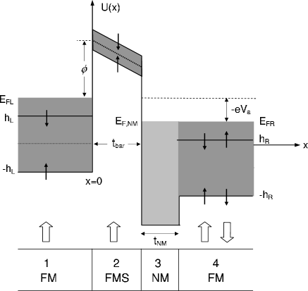
Consider a MTJ composed of two semi-infinite FM electrodes separated by a FMS layer and a NM metallic spacer, in the presence of an applied bias , as shown in Fig. 1. In the FM/FMS/NM/FM structure, the FMS layer acts as a spin filter and the NM layer as a quantum well. For simplicity, we assume the two FM electrodes are made of the same material. In the absence of any kind of scattering center for electrons, the motion along the -axis is decoupled from that of the - plane. Therefore, in the framework of the effective mass approximation, the longitudinal part of the one-electron Hamiltonian can be written as
| (1) |
where (=1-4) is the electron effective mass in the th layer, and
| (2) |
where is the Fermi energy in the left electrode. is the internal exchange energy where is the molecular field in the th FM electrode and is the conventional Pauli spin operator. The last term in Eq. (1) is a spin-dependent potential and denotes the exchange coupling between the spin of tunneling electrons and the localized spins in the FMS layer. Within the mean-field approximation, is proportional to the thermal average of the spins, (a 7/2 Brillouin function), and can be written as . Here, is the exchange constant in the magnetic barrier, and (“+” for spin-up electron and “-” for spin down one).
In order to investigate the spin transport properties in the present structure, we calculate the spin-dependent transmission coefficients, using the transfer matrix method Shok . We should note that, the transmission coefficients depend on the energy , the applied bias , the temperature , the alignment of magnetizations in magnetic layers as well as spin orientation. Therefore, the temperature and voltage dependence of current density for spin electron, in the parallel (antiparallel) alignment, can be determined as Duke :
| (3) |
where is the equilibrium Fermi-Dirac distribution at temperature . The degree of spin polarization is defined as the difference between the spin-up and spin-down current densities:
| (4) |
On the other hand, using the current densities in the parallel and antiparallel configurations, the TMR can be described quantitatively by the relative current change as
| (5) |
In our considered system, the magnetization direction of the left FM electrode and the FMS layer stays fixed, but the right FM electrode is free and may be switched back and forth by an external magnetic field, as shown in Fig. 1. Thus, the spin transport is modulated by the magnetic alignment of the right FM electrode.
III Numerical results and discussion
Numerical calculations have been carried out to investigate the effects of temperature and applied voltage on spin transport in Fe/EuS/Au/Fe structure as a typical MTJ. We have chosen Fe and EuS because they have cubic structures and the lattice mismatch is very small Dem . The relevant parameters for the Fermi energy and the internal exchange energy in the FM electrodes are chosen as =2.62 eV and =1.96 eV, which correspond to itinerant electrons in Fe Stearns . The suitable parameters for EuS as a magnetic barrier are =16.5 K Baum , =7/2, =0.1 eV Nolt , =1.94 eV Saffar2 as a symmetric barrier height, and =1.3788 nm which corresponds to four monolayer (ML) thicknesses of EuS Maug . This thickness is constant in all calculations. The Fermi energy in the Au layer is eV Kittel , and the thickness of this layer, , will be determined in terms of the interlayer distance of Au which is equal to 1ML=0.2355 nm. The effective mass of all electrons for the structure are taken as the free electron mass .
In Figs. 2 and 3, we have shown the tunneling current densities and the TMR as a function of the applied voltage at different temperatures, when . At low voltages the current densities vary linearly, whereas, with increasing the applied voltage, the effective width of the magnetic barrier becomes narrower and a nearly parabolic dependence of current on the voltage appears. These curves are typical of what is expected from Brinkman model Brink describing the tunneling free electrons. At high temperatures , there is no spin splitting of the FMS conduction band, so the magnetic barrier acts as a nonmagnetic insulator. In this case, the difference between current densities in both parallel and antiparallel configurations, and hence, the TMR effect is only due to the FM electrodes. Thus, in such temperatures the TMR has low values; see Fig. 3 at =1.2 . As the temperature decreases from , the barrier height for spin-up electrons is lowered, while it is raised for spin-down ones; thus, for a fixed applied voltage, with decreasing the temperature, the difference between current densities in the parallel and antiparallel configurations and then the TMR, increases. Both figures confirm that when the current densities in both configurations cross each other, the sign of TMR be reversed. Fig. 3 also shows that the highest value of TMR (about 270) is obtained in reverse bias and at zero temperature. This value reduces to nearly 25 in forward bias and at .
In the previous work, we showed that, with continuous variation of the NM layer thickness, the TMR oscillates with a short period equal to nm, where is the Fermi wave vector in the Au layer. In the present study, we have investigated the dependence of TMR on the NM spacer thickness at different temperatures, when changes in monolayer steps (), as it is shown in Fig. 4. It is interesting to note that, at all temperatures the TMR first increases in the first three monolayers and after that, it becomes less and starts to oscillate with a long period of approximately 2.5 nm. The value of this modification of oscillation period can be obtained from (with an integer), which is called aliasing or Vernier effect. This effect is well understood from the theory of Fourier analysis by taking into account the discrete variation of the NM spacer thickness Bruno91 ; Coe91 .
With decreasing the temperature from , the amplitude of oscillations increases, whereas, with increasing the NM layer thickness, the amplitude decreases. The origin of TMR oscillations is related to the quantum well states, formed in the NM spacer Shok .
In Fig. 5 we have displayed the spin polarization of tunneling electrons as a function of normalized temperature , for several monolayer thicknesses . At the temperatures that the FMS layer acts as a nonmagnetic insulator, the spin filtering effect in the tunnel currents is only due to the FM electrodes. Therefore, the electron spin polarization is not very high. However, at very low temperatures, the FMS layer strongly affects the TMR and spin polarization. The highest value of the spin polarization can reach 97% at zero temperature, when 3ML are used for the NM layer. With increasing the temperature, this value reduces to 60%, at . The thickness dependence of spin polarization has also shown in the inset of Fig. 5. It is obvious that, by variation of the spacer thickness, the spin polarization oscillates with a period which is equal to the oscillation period of the TMR.
It is necessary to point out that, the magnetization of FM electrodes generally depends on the temperature Mood4 . For this reason, we studied the effect of temperature on the magnetization of FM electrodes, by considering a term proportional to for this quantity. This term which has been experimentally confirmed, is applicable for surface magnetization. Since tunneling phenomenon is a surface-sensitive process, one can consider such temperature dependence for magnetization of FM electrodes. Owing to the proportionality between exchange field and the surface magnetization of the FM electrodes, we can write . The obtained results showed that, the effect of temperature variation on the magnetization of electrodes, in comparison with this effect in the FMS layer at , is very negligible, so we assumed that the FM electrodes are in completely ferromagnetic case.
Therefore, the calculated results show that, the temperature dependent spin transport is a result of the ferromagnetic phase of the FMS tunnel barrier and by adjusting the temperature, applied voltage and the thickness of NM layer, one can reach high values for the tunneling spin-polarization and TMR.
IV Concluding remarks
The temperature and voltage dependence of TMR and the spin polarization were theoretically investigated, in a new type of MTJ based on the nearly free-electron model and the transfer matrix method. Numerical results indicate that in the Fe/EuS/Au/Fe structure, due to the quantum well states and the magnetic barrier, there exist more than 260% TMR effect and about 97% spin polarization for tunneling electrons. At fixed temperature and voltage, the TMR has an oscillatory behavior as a function of the NM layer thickness. Because of the strong filtering effect of the magnetic barrier, the oscillations persist up to very large thicknesses and the period of these oscillations at all temperatures, along a fixed direction inside the Au layer, is equal.
In this study, we used of a low temperature FMS as a magnetic barrier. However, due to the recent predictions of the room-temperature FMSs Dietl , the present results may have potential utility for designing new spin electronic devices such as resonant-tunneling spin transistor and digital storage technology Yuasa .
References
- (1) D.J. Monsma, R. Vlutters, J.C. Lodder, Science 281, 407 (1998).
- (2) J.S. Moodera, L.R. Kinder, J. Nowak, P.R. LeClair, R. Meservey, Appl. Phys. Lett. 69, 708 (1996).
- (3) S.S.P. Parkin, K.P. Roche, M.G. Samant, P.M. Rice, R.B. Beyers, R.E. Scheuerlein, E.J. O’Sullivan, S.L. Brown, J. Bucchigano, D.W. Abraham, Yu Lu, M. Rooks, P.L. Trouilloud, R.A. Wanner, W.J. Gallagher, J. Appl. Phys. 85, 5828 (1999).
- (4) J.J. Sun, P.P. Freitas, J. Appl. Phys. 85, 5264 (1999).
- (5) P. LeClair, H.J.M. Swagten, J.T. Kohlhepp, R.J.M. van de Veerdonk, W.J.M. de Jonge, Phys. Rev. Lett. 84, 2933 (2000).
- (6) P. LeClair, J.T. Kohlhepp, H.J.M. Swagten, W.J.M. de Jonge, Phys. Rev. Lett. 86, 1066 (2001).
- (7) P. LeClair, B. Hoex, H. Wieldraaijer, J.T. Kohlhepp, H.J.M. Swagten, W.J.M. de Jonge, Phys. Rev. B 64, 100406 (2001).
- (8) S. Zhang, P.M. Levy, Phys. Rev. Lett. 81, 5660 (1998).
- (9) J.S. Moodera, J. Nowak, L.R. Kinder, P.M. Tedrow, R.J.M. van de Veerdonk, B.A. Smith, M. van Kampen, H.J.M. Swagten, W.J.M de Jonge, Phys. Rev. Lett. 83, 3029 (1999).
- (10) S. Yuasa, T. Nagahama, Y. Susuki, Science 297, 234 (2002).
- (11) P. LeClair, J.K. Ha, H.J.M. Swagten, C.H. van de Vin, J.T. Kohlhepp, W.J.M. de Jonge, Appl. Phys. Lett. 80, 625 (2002).
- (12) A.T. Filip, P. LeClair, C.J.P. Smits, J.T. Kohlhepp, H.J.M Swagten. B. Koopmans, W.J.M. de Jonge, Appl. Phys. Lett. 81, 1815 (2002).
- (13) D.C. Worledge, T.H. Geballe, J. Appl. Phys. 88, 5277 (2000).
- (14) M. Wilczyński, J. Barnaś, R. Świrkowicz, J. Magn. Magn. Mater. 267, 391 (2003).
- (15) A. Saffarzadeh, J. Phys.: Condense Matter 15, 3041 (2003).
- (16) A. Saffarzadeh, J. Magn. Magn. Mater. 269, 327 (2004).
- (17) A.A. Shokri, A. Saffarzadeh, J. Phys.: Condens. Matter 16, 4455 (2004).
- (18) J.S. Moodera, X. Hao, G.A. Gibson, R. Meservey, Phys. Rev. Lett. 61, 637 (1988).
- (19) X. Hao, J.S. Moodera, R. Meservey, Phys. Rev. B 42, 8235 (1990).
- (20) C.B. Duke, in Tunneling Phenomena in Solids edited by E. Burstein, S. Lundquist (Plenum, New York, 1969).
- (21) U. Rücker, S. Demokritov, R.R. Arons, P. Grünberg, J. Magn. Magn. Mater. 269-270, 156 (1996).
- (22) M.B. Stearns, J. Magn. Magn. Mater. 5, 167 (1977).
- (23) G. Baum, E. Kisker, A. H. Mahan, W. Raith and, B. Reihl, Appl. Phys. 14, 149 (1977).
- (24) W. Nolting, U. Dubil, and M. Matlak, J. Phys. C: Solid State Phys. 18, 3687 (1985).
- (25) A. Mauger, C Godart, Phys. Rep. 141, 51 (1986).
- (26) C. Kittel, in Introduction to Solid State Physics 6th ed. (John Wiley & Sons, New York, 1986).
- (27) W.F. Brinkman, R.C. Dynes, J.M. Rowell, J. Appl. Phys. 41, 1915 (1970).
- (28) P. Bruno, C. Chappert, Phys. Rev. Lett. 67, 1602 (1991); Phys. Rev. B 46, 261 (1992).
- (29) R. Coehoorn, Phys. Rev. B 44, 9331 (1991).
- (30) C.H. Shang, J. Nowak, R. Jansen, J.S. Moodera, Phys. Rev. B 58, R2917 (1998).
- (31) T. Dietl, H. Ohno, F. Matsukara, J. Cibert, D. Ferrand, Science 287, 1019 (2000).