Detection of Single Electron Charging in an Individual InAs Quantum Dot by Noncontact Atomic Force Microscopy
Abstract
Single electron charging in an individual InAs quantum dot was observed by electrostatic force measurements with an atomic force microscope (AFM). The resonant frequency shift and the dissipated energy of an oscillating AFM cantilever were measured as a function of the tip-back electrode voltage and the resulting spectra show distinct jumps when the tip was positioned above the dot. The observed jumps in the frequency shift, with corresponding peaks in dissipation, are attributed to a single electron tunneling between the dot and the back electrode governed by Coulomb blockade effect, and are consistent with a model based on the free energy of the system. The observed phenomenon may be regarded as the “force version” of the Coulomb blockade effect.
pacs:
68.37.Ps, 73.21.La, 73.22.-fSelf-assembled semiconductor quantum dots (SAQDs) grown by lattice mismatched heteroepitaxy have attracted much attention as a promising system for many applications such as lasers, information storage devices and quantum computation. There have been a considerable number of studies on the single electron charging effects on SAQDs located in field-effect structures because they enable the control of the charging state in the QDs by external electric fields. These states can be probed by capacitance spectroscopy Drexler et al. (1994) which provides information on the energy level structure as well as the charging energy of the QDs Miller et al. (1997). However, capacitance spectroscopy probes an ensemble of dots and cannot be applied to an individual QD. Access to individual QDs is considered to be a key technique not only for the further understanding of the physics of QDs, but also for some practical applications such as information storage and qubit read-out in quantum computation.
Scanning tunneling spectroscopy (STS) has been employed to investigate a single QD Banin et al. (1999); Maltezopoulos et al. (2003). However, application of STS is limited to uncapped QDs on conducting substrates since a tunneling current greater than 1 pA is usually required. Electrostatic force measurement by atomic force microscopy (AFM) is known to have single electron sensitivity Schonenberger and Alvarado (1990); Klein and Williams (2001, 2002). In these experiments, the observation of single electrons is based on the observation of quantized jumps in the force signal. Recently spectacular results on a QD incorporated in a carbon nanotube (CNT) were reported Woodside and McEuen (2002). To determine single charging effects in these experiments, corroborating transport measurement through the QD via the CNT leads were necessary. This is unfortunately limiting for many interesting systems such as SAQDs or suspected charge traps leading to noise in mesoscopic devices, as contact leads cannot easily be attached. In this Letter, we report the observation of single electron charging events of a single SAQD by electrostatic force measurement and present a simple theoretical model which explains the main features of the experimental results. As a consequence, optimal sample geometries can be designed and expected signal levels predicted for the experimental detection of single charging events. In addition we observe strong variations in the AFM force sensor damping, which demonstrate the potential of this technique to investigate the fascinating interactions between micromechanical oscillators and single electron systems Schoelkopf et al. (1998); Knobel and Cleland (2003); Clerk et al. (2002).
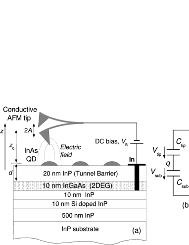
The samples were prepared on a semi-insulating InP wafer by chemical beam epitaxy Poole et al. (2001). The schematic of the sample structure is depicted in Fig. 1. The SAQDs spontaneously form due to lattice mismatched heteroepitaxy. A two dimensional electron gas (2DEG) formed in the InGaAs quantum well was used as a back electrode located 20 nm underneath the InAs SAQDs layer. The electrical contact to the 2DEG was made by indium diffusion and low resistance Ohmic characteristics were confirmed between two such contacts at 4.2 K. The sample used in this experiment has a single layer of uncapped InAs SAQDs with a small dot density (5 ). The typical dot is nm in diameter and 12 nm in height. In order to probe individual QD, we used an AFM in the frequency modulation mode Albrecht et al. (1991).
In this technique, the AFM cantilever is self-oscillated at its mechanical resonance frequency by a positive feedback circuit with a phase shifter and the resonance frequency shift caused by the tip-sample interaction is measured by a phase locked loop Nan . The oscillation amplitude, , of the tip is held constant at 5 nm with an automatic gain controller (AGC). This enables the measurement of dissipation in the cantilever oscillation simultaneously to . Our home-made cryogenic AFM Roseman and Grutter (2000) uses a fiber-interferometric deflection sensor and has been previously used for successful imaging of vortices on Nb Roseman et al. (2001). The experiments were performed at 4.2 K in high vacuum of . The cantilever used in our experiment had a resonance frequency, , of 150 kHz with a spring constant, , of 15 N/m. The tip was coated with a 10 nm Ti/ 20 nm Pt to ensure good electrical conductivity at 4.2 K. After identifying a single QD by AFM by noncontact imaging, we performed series of electrostatic force spectroscopy (EFS) over the QD as a function of tip-sample separation. This spectroscopy records the change in the resonance frequency of the cantilever, , caused by the tip-sample interaction as a function of the bias voltage between the tip and the back electrode while the distance regulation is turned off. The average tip-QD distance is typically more than 10 nm so that the tunneling between the tip and the QD is negligible and the electrostatic force is the dominant interaction.
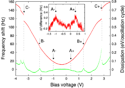
Figure 2 shows a typical EFS spectrum and the dissipation signal. The overall shape of the spectrum is characterized by a parabola which reflects the capacitive force between the tip and the back electrode. Since this force is attractive, the resonant frequency shift is negative. For clarity, the negative frequency shift is plotted in all the following figures. The minimum frequency shift at non-zero bias accounts for the contact potential difference between the tip and the sample. In addition to the parabolic background, some jumps are found in the frequency shift at various bias voltages. We attribute them to the discrete change in the electrostatic force due to sequential charging of a single QD by a single electron tunneling between the QD and the back electrode (Coulomb blockade). These Coulomb blockade (CB) jumps are also observed in the dissipation signal as peaks at the same bias voltages. The increase in dissipation is obviously related to the dissipated energy in the electron tunneling process. This correspondence is helpful to identify the CB jumps at a lower bias voltage whose frequency shift counterpart tends to be identified with difficulty. No structure like those mentioned above were observed on the sample without the QD.
We consider a simple model based on the free energy of the system as depicted in Fig. 1(b) to calculate the force acting on the AFM tip. The free energy consists of the electrostatic charging energy and the work done by the voltage source and can be expressed as Waser (2003):
| (1) |
Here is the charge residing in the QD. and are the QD-substrate, the tip-QD capacitance and , respectively. The force acting on the tip can be obtained by where is the tip-QD distance. Then we get
| (2a) | |||||
| (2b) | |||||
where . The first term accounts for the interaction between the charge in the QD and its image charge in the tip but it is negligibly small under our experimental conditions. The third term shows the parabolic background and accounts for the interaction between the polarized charges in the tip and the back electrode. The interaction between the charge in the QD and the polarized charge in the tip is actually included in the second term and is responsible for the detection of the charge in the QD. It should be noticed from Eq. (2b) that the expression reduces to a simple parabola when is independent of .
In this system, unlike the double tunneling junction which has been investigated by STS, only an electron tunneling between the back electrode and the QD is possible because of the large tip-QD distance. For this tunneling to be possible, the final state must be energetically favorable. This requires for an electron to tunnel onto the QD with electrons, and for an electron to tunnel off the QD with electrons. This determines the bias range (Coulomb blockade) in which the electron tunneling is forbidden:
| (3) |
This translates into the condition, which relates the charging energy of the QD, , to the applied voltage to the QD through the relation, . Eq. 3 leads to
| (4) |
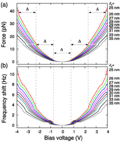
where the function gives the nearest integer to the argument. By combining Eq. (2a) and Eq. (4), the force can be obtained as a function of the bias voltage. The calculated - curves are shown in Fig. 3(a) for various . Step-like structures are found on the parabolic background. The distance between two neighbouring jumps is constant and given by . The step height increases at higher bias voltages because it is proportional to the as can be seen in the second term of Eq. (2a). This means that the structure nearer the zero bias is harder to observe. A closer look at Eq. (2a) shows that decreasing (increasing the distance between the QD and the back electrode) enhances the jumps and reduces the parabolic background. Note that increasing the QD-back electrode separation decreases the tunneling rate.
The resonant frequency shift of the cantilever measured in EFS is related to the force through the relationship Giessibl (2001):
| (5) |
The frequency shift is a weighted average of the force over one oscillation period. The calculated - curves are shown in Fig. 3(b). Although the step in - curve translates into broader increase in because of the averaging, the onset of the increase still corresponds to the step in - curve at the closest distance in one oscillation period. This allows us to determine from - curves using Eq. (3).
When we look at Fig. 2 carefully, the spacings between two neighboring jumps are not exactly the same. One reason is that the oscillation amplitude decreases around the jumps due to feedback errors of the AGC. The decrease in the amplitude leads to an increase in the closest tip-QD distance which results in the shift of the jumps to higher bias voltage. The significant decrease in amplitude was actually observed at jump B and C, respectively. The sharper increase at jump C is also due to the smaller amplitude. The shift of the jump due to this effect should be corrected in order to investigate the detail of the spectra, such as internal energy levels of the QD where the separations between neighboring jumps are of serious concern. Regardless, we focus on the tip-QD distance dependence of the jump B to demonstrate that the observed feature is consistent with the theory discussed above.
Figure 4(a) shows a series of EFS spectra taken over a QD at various tip-QD distances.
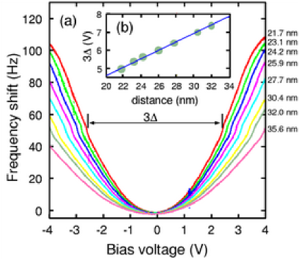
As expected from the theory, the jump shifts to the lower bias voltage as the distance becomes smaller because of the larger . Assuming that the spacing between B+ and B- is equal to , is found to range from 0.064 to 0.094 aF. This is one order of magnitude smaller than that in the STS experiment. In STS such a small value is not permissible because of associated low tunneling rate which is far less than that equivalent to a current of 1 pA. In other words, the electrostatic force detection is sensitive to even a single electron charging event unlike STS measurements which statistically average a large number of such events. Larger in the experiment than the calculated one is attributed to the electrostatic force between the tip and the substrate around the QD which is not taken into account in the calculation. It also accounts for less sharp jumps in the experimental spectra.
As is shown in Fig. 4(b), the spacing between the jumps B+ and B-, is linearly dependent on the tip-QD distance. This indicates and it implies that the parallel plate capacitor model is valid in this distance range. Using a linear fitting of versus distance plot, the absolute tip-QD distance and the effective area of the QD can be determined. The resulting distance ranges from 22 to 42 nm and the effective QD diameter is 17 nm. The discrepancy between the effective and the measured diameter is due to the parallel plate approximation of the lens shape QD as well as a depletion layer likely formed on the QD surface by surface oxidation which affects the effective size of the QD. These jumps and the corresponding peaks were also observed in - curves and in the dissipation- curves at a fixed bias voltage (data not shown here). This can be understood by considering the change in along with Eq. (4) and it provides additional evidence for the observation of single electron effects. The correlation of the peak in the dissipation with the jumps in the EFS spectra is also a good indication of the electron hopping on and off the QD with the oscillating tip. Joule dissipation of moving charges has been reported previously Denk and Pohl (1991); Stowe et al. (1999), but a quantitative calculation of the theoretically expected dissipation is more than an order magnitude off. We are presently investigating if the backaction of single electron charging events on the micromechanical oscillator can account for the observed dissipation.
In conclusion, we detected a single electron charging of an individual InAs QD by electrostatic force measurement. The observed features could be explained by a simple theory based on consideration of the free energy of the tip-QD-back electrode system. This theoretical understanding allows the optimization of sample geometries (in particular the back electrode to QD spacing). This will enable experimental investigation of single charging events in diverse systems such as SAQDs and charge traps in mesoscopic systems. In contrast to STS, this technique can be used to investigating a QD only weakly coupled to an external electrode. Finally, we have observed strong contrast in dissipation, which cannot be explained by classical Joule dissipation. We currently only speculate that this is due to back action effects of single electron charging events on the micromechanical AFM oscillator.
This research was supported by the Natural Science and Engineering Research Council of Canada, the Canadian Institute of Advanced Research, and NanoQuébec.
References
- Drexler et al. (1994) H. Drexler, D. Leonard, W. Hansen, J. P. Kotthaus, and P. M. Petroff, Phys. Rev. Lett. 73, 2252 (1994).
- Miller et al. (1997) B. T. Miller, W. Hansen, S. Manus, R. J. Luyken, A. Lorke, J. P. Kotthaus, S. Huant, G. Medeiros-Ribeiro, and P. M. Petroff, Phys. Rev. B. 56, 6764 (1997).
- Banin et al. (1999) U. Banin, Y. Cao, D. Katz, and O. Millo, Nature 400, 542 (1999).
- Maltezopoulos et al. (2003) T. Maltezopoulos, A. Bolz, C. Meyer, C. Heyn, W. Hansen, M. Morgenstern, and R. Wiesendanger, Phys. Rev. Lett. 91, 196804 (2003).
- Schonenberger and Alvarado (1990) C. Schonenberger and S. F. Alvarado, Phys. Rev. Lett. 65, 3162 (1990).
- Klein and Williams (2001) L. Klein and C. Williams, Appl. Phys. Lett. 79, 1828 (2001).
- Klein and Williams (2002) L. Klein and C. Williams, Appl. Phys. Lett. 81, 4589 (2002).
- Woodside and McEuen (2002) M. Woodside and P. McEuen, Science 296, 1098 (2002).
- Schoelkopf et al. (1998) R. J. Schoelkopf, P. Wahlgren, A. A. Kozhevnikov, P. Delsing, and D. Prober, Science 280, 1238 (1998).
- Knobel and Cleland (2003) R. G. Knobel and A. N. Cleland, Nature 424, 291 (2003).
- Clerk et al. (2002) A. A. Clerk, S. M. Girvin, A. K. Nguyen, and A. D. Stone, Phys. Rev. Lett. 89, 176804 (2002).
- Poole et al. (2001) P. Poole, J. McCaffrey, R. L. Williams, J. Lefebvre, and D. Chitrani, J. Vac. Sci. Technol. B19, 1467 (2001).
- Albrecht et al. (1991) T. R. Albrecht, P. Grutter, D. Horne, and D. Ruger, J. Appl. Phys. 69, 668 (1991).
- (14) Nanosurf AG, Liestal, Switzerland.
- Roseman and Grutter (2000) M. Roseman and P. Grutter, Rev. Sci. Inst. 71, 3782 (2000).
- Roseman et al. (2001) M. Roseman, P. Grutter, A. Badia, and V. Metlushko, J. Appl. Phys. 89, 6787 (2001).
- Waser (2003) R. Waser, ed., Nanoelectronics and information technology: Advanced electronic materials and novel devices (John Wiley & Sons, 2003), chap. Single-electron devices for logic applications.
- Giessibl (2001) F. J. Giessibl, Appl. Phys. Lett. 78, 123 (2001).
- Denk and Pohl (1991) W. Denk and D. W. Pohl, Appl. Phys. Lett. 59, 2171 (1991).
- Stowe et al. (1999) T. D. Stowe, T. W. Kenny, D. J. Thomson, and D. Rugar, Appl. Phys. Lett. 75, 2785 (1999).