Total Angular Momentum Conservation During Tunnelling through Semiconductor Barriers
Abstract
We have investigated the electrical transport through strained double-barrier resonant tunnelling diodes. The confinement shift for diodes with different well width, the shift due to a central potential spike in a well, and magnetotunnelling spectroscopy demonstrate that the first two resonances are due to tunnelling through heavy hole levels, whereas there is no sign of tunnelling through the first light hole state. This demonstrates for the first time the conservation of the total angular momentum in valence band resonant tunnelling. It is also shown that conduction through light hole states is possible in many structures due to tunnelling of carriers from bulk emitter states.
pacs:
72.25.Dc, 73.40.GkThe challenge of introducing spin as an additional degree of freedom in semiconductor devices has lately attracted great attention.Prinz ; Wolf One approach to couple the spin to the carrier motion is through the spin-orbit interaction; one suggestion is to use it in conjunction with resonant tunnelling devices (RTDs) for injection and detection of spin currents.Hall ; Glasov Whereas the spin-orbit coupling in the conduction band, mediated by the Dresselhaus mechanism Dresselhaus ; Malcher or the Rashba mechanism,Bychkov is generally rather weak, the interaction is strong in the valence band. Since this band is made up from p-orbitals, the interaction term is non-zero, and there is a strong coupling between the orbital angular momentum and the spin , so that the total angular momentum is a proper eigenvalue at the band edge. luttinger In order to examine the feasibility of such devices for spintronics applications, one may therefore already consider spin (or ) detection in p-RTDs. It is then rather disconcerting to find, that in all previous investigations, tunnelling has been observed from heavy hole states (HH; with at ) to light hole states (LH; ) or split-off states (SO, ).Mendez ; Liu ; Lewis ; Hayden ; Gennser1 It has been proposed that this non-conservation of the total angular momentum in resonant tunnelling is due to either the band mixing at finite in-plane momentum , or because of interface roughness scattering. However, especially in strained quantum wells, the non-parabolicity and band mixing for the lowest states is quite small. This suggests that scattering plays a large role even in systems with interfaces known for their good quality. In our present study, we show the absence of resonances in the characteristics from heavy holes tunnelling through the first light-hole state in a double barrier p-type quantum well. This demonstrates conclusively that there is conservation during resonant tunnelling. Furthermore, by investigating specially designed RTDs, we are able to show that the emitter structure away from the barrier interface may explain an apparent mixing of in the tunnelling process.
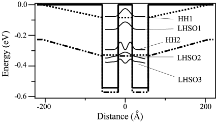
The samples were grown by molecular beam epitaxy on fully relaxed Si0.5Ge0.5 pseudosubstrates, of which the top 2 m is p-doped, . The active part of the initial structures consist of Å barriers surrounding a single Si0.2Ge0.8 quantum well (QW) of width (, , or Å for three different samples). Symmetrically on either side of the active structure are Å thick SiGe emitter layers that are linearly graded, from % Ge closest to the barriers to % Ge away from the barriers. These emitter layers consists of an undoped spacer (Å, closest to the barriers) and a doped part (Å, ). A Å, Si0.5Ge0.5 top contact layer terminates the structure. The corresponding structure for the Å QW is schematically shown in Fig. 1. For clarity, the graded emitter region is also shown, and the lowest energy levels in the quantum well at are indicated. Due to the strain splitting, only HH states will be populated in the emitter closest to the barrier. Since the LH and SO bands are coupled even for zero in-plane momentum , we have denoted these states as LHSO; however, the LHSO1 level is in fact predominately LH.
The diodes were processed into mesas with diameters varying between and . All measurements were performed at K, using separate voltage and current leads connected to both diode contacts, unless otherwise stated. However, we found that the resonance voltages changed by less than % between 4K and 77K.
In Fig. 2a the 77K current versus voltage characteristics of the three different RTDs are plotted. They show up to three resonances, with a maximum peak-to-valley current ratio of at K. These characteristics are comparable to the best p-type RTDs in any material system, and indicate a good interface quality minimizing interface-roughness assisted tunnelling. In the following we will focus on the two lowest resonances.
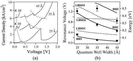
The first evidence for assigning the resonances comes from the confinement shift clearly evident in the characteristics. The shift, obtained from measurements of the smallest diodes, is unaffected by the contact layer resistance from the substrate, as verified by the dependence of the current on the mesa size. In Fig. 2b the resonance voltages vs. well width are plotted. On the right hand scale, these are compared with the calculated energies. The scales can be directly compared by assuming a linear voltage drop across the double barriers, the quantum well and the undoped part of the structure. Including the Stark changes the energies much less than the measurement uncertainties. Because of the graded nature of the emitter, the zero bias emitter states lie 30 meV higher then than the quantum well edge. This is included as an energy offset between the two scales. The so-called ’lever arm’ - i.e. the ratio between the energy drop between the emitter and the centre of the quantum well and the applied voltage - is in good agreement with what can be expected from geometrical considerations, and the energies are consistent with those obtained from intersubband absorption measurements.Diehl A good agreement between theory and experiment is found if the first two resonances correspond to tunnelling through the HH1 and HH2 states, respectively. Moreover, the difference between the first two resonances increases with decreasing well width. This effect is only obtained for states with different index, such as HH1 and HH2.
In view of the simplicity of the model - e.g. neither depletion width nor carrier accumulation in the structure is taken into account - this result alone can only be taken as an indication of the nature of the resonances. However, support for the model is found through magnetocurrent oscillations. For low, fixed and with a magnetic field applied parallel to the current, it is possible to observe weak oscillations periodic in (period ). They are due to Landau levels passing through the quasi-Fermi energy in the emitter accumulation layer, the two-dimensional charge density of which is . Unlike similar oscillations in GaAs/AlAs p-type RTDs Hayden2 , no decrease in is found as passes through the resonances, from which we conclude that the charge density in the quantum wells is negligible. Furthermore, the electric field over the QW structure is in reasonable agreement with the simple lever arm model.
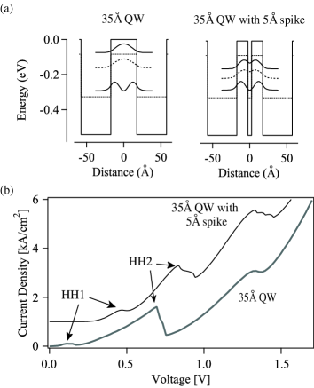
Further, conclusive evidence that the above assignment of the resonances is correct can be found in experiments where the resonances are shifted by a central potential spike. Even symmetry states (HH1, LHSO1), with a wave function maximum in the middle of the quantum well, are much more affected by a central, repulsive potential spike than odd symmetry states (HH2, LHSO2).JYM In our samples, the spike has been approximated by a thin Si layer; a Å QW with a Å spike in the middle was investigated and compared to the initial Å structure (Fig. 3a). The plotted wavefunctions in the figure give a clear picture of the described effect. An example of the characteristics measured at 77K is displayed in Fig. 3b) and clearly demonstrate the predicted behaviour for the HH1 and HH2 states. We find shifts for the first and second resonances equal to and , respectively, where the uncertainty is due to the natural scatter of the measured resonances for different diodes of the same structure. The values compares well with the calculated values (using the model described above, including Stark shifts) of and for the HH1 and HH2 resonance respectively.HH1 In contrast, assuming a lever arm compatible with the second resonance due to LHSO1 tunnelling, the expected shift would be .
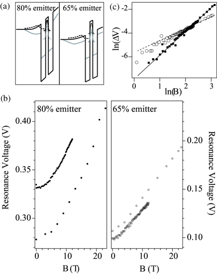
Having shown that it is possible to observe -conservation in these tunnelling experiments, we now try to understand the difference between the present samples and those of previous studies, where tunnelling through LHSO states was observed. One important contrast is the higher strain used in the present study. For example, in previous studies of Si/SiGe RTDs on Si substrates, the Ge content was around . Liu ; Gennser1 One consequence is that the HH and LHSO states in the emitter were less decoupled in these samples, with a separation between the HH and LH potentials meV, whereas for the present samples it is meV. To study the role of the emitter, a structure with a Å QW and an emitter region with a grading from % to % was investigated (See Fig. 4(a)). Two resonances, at 100 mV and 470 mV, are observed in this ’emitter ramp’ sample. The second resonance voltage is compatible with the estimated resonance voltage of the tunneling through HH2 but the first resonance is likely due to the tunneling through LHSO1: the tunneling through HH1 is prohibited by design. Also the 370 mV separation between the two resonances is more than a factor of 2 smaller than the separation between the HH 1 and the HH2 resonances of % emitter sample (Fig.2).
To further compare these resonances, we use magnetotunnelling spectroscopy with up to 23 T. A magnetic field applied perpendicular to the current accelerates the carriers in the direction perpendicular to both and , so that they tunnel through the quantum well levels at a non-zero in-plane momentum, centered around where is the tunnelling distance.Hayden The in-plane dispersion relations can then be mapped out and compared with the calculated dispersion .Hayden ; Hayden2 ; Gennser1 ; Gassot All the HH1 resonances of the three regular structures show a parabolic behaviour. The corresponding effective masses (0.04 , 0.15 , and 0.13 for the Å, Å and Å wells, respectively) are in reasonable agreement with the calculated dispersions (0.17 , 0.155 , and 0.144 ) though quantitative comparisons are difficult to make. Hayden2
In Fig. 4(b) we compare the shift for the first resonance of the sample with a Å QW and an 80 emitter and of the emitter ramp sample. In contrast to the 80 emitter resonance, the first resonance of the emitter ramp sample shows a very distinct linear behaviour. A log plot clearly demonstrates these dependences (Fig. 4c). This indicates that it is the first resonance rather than the second that is not due to tunnelling through one of the HH states. Furthermore, a magnetic field cannot lead to a linear energy shift of the valence band QW states or the emitter states next to the barrier. The Zeeman effect is given by (plus a small term proportional to ) Luttinger , which is only a small perturbation since the direction of is frozen in the direction of the confinement and the strain. Since the well thickness is much smaller than the cyclotron orbit even for the highest fields, Landau level formation can also be excluded. Neither can the linear shift in Fig. 4 be explained by the acceleration in k-space, since the levels are quite parabolic, and never linear in . In fact, we find that only an unstrained valence band bulk state can give rise to the observed linear shift. We propose that there are two reservoires of holes in the emitter: states confined close to the Si barrier and states in the unstrained ’bulk’ part of the emitter. The latter, tunnelling through the LHSO1 state, are responsible for the first resonance of the ramp emitter sample. In the bulk the vector is free to turn along the B-field axis, and with perpendicular to the growth axis, the quantum well state will ’see’ a mixed HH-LHSO state coming from the emitter. Because of the lower Ge content in this emitter, the barrier for the holes from the bulk is smaller, making it possible for them either to tunnel directly into the quantum well states, or to form hybrid states with the emitter states in the HH emitter well. The Landau level separation in the Si0.5Ge0.5 bulk is 0.6 meV/T, and the Zeeman energy a factor of 2-10 smaller.Winkler This compares reasonably well with the measured slope of 4.1 mV/T 1.4 meV/T. It seems plausible that the apparent tunnelling from HH to LHSO states in other p-type RTDs may be due to the inevitable bulk part of the emitter, as well as band mixing in the well states. A similar linear behaviour has indeed been observed in a Si/Si0.75Ge0.25 RTD with the strain fully in the SiGe layer. Gassot
Concerning the third resonance of the Å and Å sample, the fit with the energy levels in Fig. 2 indicates that it corresponds to tunnelling through the second LH-like state (LHSO3 in the figure), and this also agrees with the observed shift in the sample with a central Si spike. This state is much less parabolic than the three lower states, and one would therefore expect a larger amount of band mixing. However, further experiments are necessary to confirm this.
We have demonstrated that the total angular momentum is conserved during resonant tunnelling in a system with strong spin-orbit coupling. This does not necessarily imply that the same holds true for the case of weakly coupled spin, but is certainly an encouraging sign. However, it may also have direct implications for the field of spintronics, since in order to inject spin in a semiconductor, a possible path is through the growth of magnetic semiconductors as electrodes. Much of the work has been focused on GaMnAs alloys, where the Mn not only provides the ferromagnetic properties, but also is a p-dopant.Dietl ; Mattana Finally, it should also be noted that these results may have an additional relevance for the development of a Si/SiGe based quantum cascade laser, in they exclude one of the possible non-radiative conduction paths for the HH carriers in these structures.Gennser2
Acknowledgements.
We would like to thank J. Faist for help with this work. It has been partly financially supported by the Swiss National Science Foundation, the EC Contract Si-GeNET, ”Région Ile de France”, ”Conseil Général de l’Essonne” and the program Nano2008.References
- (1) G. Prinz, Science 282, 1660 (1998).
- (2) S. A. Wolf, Science , 294, 1488 (2001).
- (3) K. C. Hall, , Appl. Phys. Lett. 83, 2973 (2003).
- (4) M. M. Glasov, , cond-mat 0406191 (2004).
- (5) G. Dresselhaus, Phys. Rev. 100. 580 (1955).
- (6) F. Malcher, G. Lommer, and U. Rœssler, Superlatt. Microstr. 2, 267 (1986).
- (7) Y. Bychkov and E. Rashba, JETP Lett. 39, 78 (1984).
- (8) J. M. Luttinger and W. Kohn, Phys. Rev. 97, 869 (1965).
- (9) E. E. Mendez, W. I. Wang, B. Ricco, and L. Esaki, Appl. Phys. Lett. 47, 415 (1985).
- (10) H. C. Liu, D. Landheer, M. Buchanan, and D. C. Houghton, Appl. Phys. Lett. 52, 1809 (1988).
- (11) R. M. Lewis, H. P. Wei, S. Y. Lin, and J. F. Klem, Appl. Phys. Lett. 77, 2722 (2000).
- (12) R.K. Hayden, , Phys. Rev. Lett. 66, 1749 (1991).
- (13) U. Gennser, , Phys. Rev. Lett. 67, 3828 (1991).
- (14) L. Diehl, , Appl. Phys. Lett. 80, 3274 (2002).
- (15) R.K. Hayden, , Semicond. Sci. Technol. 7, B413 (1992).
- (16) J.-Y. Marzin and J.-M. Gérard, Phys. Rev. Lett. 62, 2172 (1989).
- (17) The larger discrepancy for the HH1 is expected since it is more sensitive to the exact thickness of the Si spike.
- (18) P. Gassot, , Physica E 2, 758 (1998).
- (19) J. M. Luttinger, Phys. Rev. 102, 1030 (1956).
- (20) The value depends on the interpolation used between Si and Ge. See R. Winkler, M. Merkler, T. Darnhofer, and U. Rœssler, Phys. Rev. B 53, 10858 (1996).
- (21) T. Dietl, , Science 287, 1019 (2000).
- (22) R. Mattana, , Phys. Rev. Lett. 90, 166601 (2003).
- (23) U. Gennser, , in ’Future Trends in Microelectronics’, Ed. S. Lyuri, J. Xu, and A. Zaslavsky (Wiley-IEEE Press, 2004).