Growth of Tellurium on As-exposed Si(211)
Abstract
Electronic structure calculations are performed to obtain the As-exposed Si(211) and the Te adsorbed As-exposed Si(211) surface. Arsenic-exposed Si(211) may be obtained by adsorbing As on Si(211) or by replacing surface Si atoms by As. First, we carry out systematic investigations to obtain stable As-exposed Si(211) due to As adsorption at various coverages. We find that at 1/2 monolayer (ML) coverage of As, the highly terraced Si(211) surface becomes flat decorated with parallel As chains extending along the [] direction. At 1 ML coverage the Si surface essentially retains its ideal structure with an added layer of As. Motivated by the adsorption sequence in the HgCdTe (MCT) growth on Si, Te adsorption on such an As-exposed Si(211) is studied and 1/2 ML of Te coverage is found to be energetically feasible. Next, we explore a stable As-exposed Si(211) upon replacement of surface Si atoms by As. An energetic comparison reveals that the As-exposed Si(211) obtained by replacing surface Si atoms with As is more favorable compared to that obtained by adsorbing As on Si(211). In line with the adsorption sequence in the MCT growth on Si, Te is then adsorbed on the most favorable As-exposed Si(211) and in contrast to earlier situation, Te coverage here is found to be 1/4 of ML which agrees with the experiment.
pacs:
71.15Mb,68.43Bc, 68.43FgI Introduction
As technological devices are often developed on Si substrates, Si surfaces continue to be a subject of intense theoretical and experimental studies. Extensive investigations have been done on the low index Si surfaces, for example, Si(001) and Si(111). book1 ; book2 Most of the theoretical investigations have been confined to low index surfaces due to the ‘simplicity’ of the surface. However, the high index surfaces, Si(211), Si(311), Si(331), Si(557), and Si(553), have attracted some attention recently chadi ; olshanetsky ; nibir0 ; rujirawat ; yang ; smith ; thesis ; baski0 ; baski ; baski1 ; baski2 ; himpsel1 ; WKI ; berghaus ; wang ; kaplan ; sen . High index surfaces play technologically important role as substrates for the fabrication of long wavelength infra-red detectors rujirawat ; yang ; smith ; thesis and as substrates for the formation of metallic nanowires baski1 ; baski2 ; himpsel1 .
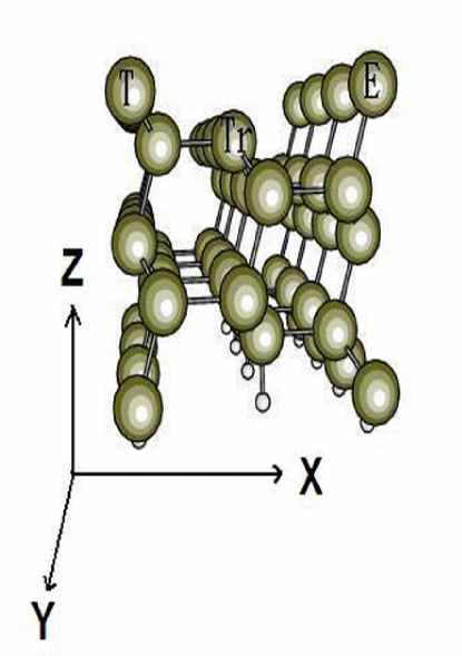
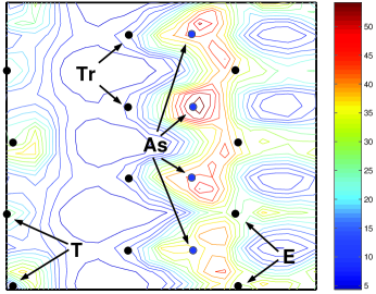
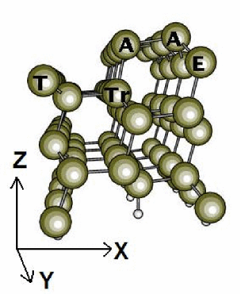
Many of the high index Si surfaces are complicated in structure due to the existence of terraces and steps. The surface of interest here is Si(211) which can be looked upon as stepped arrangement of narrow (111) terraces. A three dimensional view of a small portion of the ideal Si(211) surface is shown in Fig. 1. The atoms marked T (called the terrace atoms) on the terrace are three-fold coordinated and thus have one dangling bond each; those on the step edge, marked E (called the edge atoms) are two-fold coordinated and have two dangling bonds each. Atoms in the second layer and closest to the edge atoms are denoted as Tr (called the trench atoms) have one dangling bond each. The Si(211) surface consists of two-atom wide terraces between terrace and edge atoms along the [] direction. Two consecutive terraces are separated by steps and are 9.4 Å apart in the [] direction, while they extend infinitely along [].
The Si(211) surface is now one of the surfaces of choice for epitaxial growth of polar (both III-V and II-VI) semiconductors on Si. It has been shown earlier WKI that the Si(211) surface leads to a better quality epitaxial growth of GaP as compared to Si(001) because it satisfies both the requirements of interface neutrality and offering inequivalent favorable binding sites for Ga and P. The Si(211) surface has atoms with both one and two dangling bonds. The atoms with two dangling bonds can accommodate P, whereas Ga binds with Si(211) that has a single dangling bond. Large area high quality CdTe layers have also been grown on the Si(211) surface for subsequent growth of HgCdTe. rujirawat ; yang ; smith In particular, our motivation for studying Si(211) is due to emerging experimental interest in epitaxial growth of HgCdTe after a successive growth of ZnTe and CdTe on the As-exposed surfaces aiming at the development of large area focal plane arrays for the fabrication of detectors. thesis
As far as the reconstruction of Si(211) is concerned there have been several studies.berghaus ; wang ; kaplan ; sen However, a recent study by Baski et al. baski0 ; baski was conclusive where the authors showed in their STM images that the clean Si(211) is unstable and it consists of nanofacets with (111) and (337) orientations. As there are evidences baski1 that the (211) orientation is regained due to metal adsorption on Si(211), we will use the bulk terminated surface to study the the As adsorption on Si(211). In addition, we will extend our study to understand the atomic configurations of Te on the As-exposed Si(211).
It has been established in recent experiments thesis ; romano that the epitaxial growth of II-IV materials on an As terminated Si surface gives a better quality film compared to that on a bare Si surface. For example, high quality interface and better ZnS films were obtained romano with As-exposed Si(001). A better quality MCT growth is possible after a successive growth of ZnTe and CdTe on the As-exposed Si(111) and Si(211) surfaces. thesis ; chad So far, we do not have a comprehensive understanding of the interaction and atomic configuration of As on the Si(211) surface. We therefore, carry out extensive electronic structure calculations for As adsorption on the Si(211) surface at various coverages. Here we note that an earlier study sen to understand the interaction of As on Si(211) revealed important results but was incomplete. There are speculations brill based on the analysis by Bringans bringans that As atoms may replace surface Si atoms instead of being adsorbed on Si(211). So, we perform further calculations by replacing the terrace, trench and edge Si atoms by As. Comparing all the results and also based on physical grounds we provide the energetically favorable surface structures and As positions on the Si(211) surface at various coverages.
Recently nibir , Auger-electron spectroscopy was used to determine the Te coverage on an As-exposed Si(211) surface and it was found that only approximately 20-30 % of a monolayer (ML) of Te is bonded to the Si(211) surface. This experimental result encouraged us to further carry out energetic calculations for the Te adsorption on the As-exposed Si(211). Our total energy calculations reveal that Te coverage on the As-exposed Si(211) is preferably 25% of 1 ML which agrees with the experimental result.nibir To the best of our knowledge, no such calculations exist in the literature.
The paper is organized as follows. In Section II we present the parameters used in the pseudopotential density functional calculations. The results and discussions are presented in Section III. The results for the As adsorption on the Si(211) are presented in subsection III.1. Subsection III.2 gives the results for the Te adsorption on the As adsorbed Si(211), III.3 contains the results for Si replacement by As and III.4 give results for Te adsorption on Si(211) surfaces with all the terrace and trench Si atoms being replaced by As. And finally, in section IV, we summarize our principal results.
II Method
Total energy minimization calculations are carried out within the density functional theory (DFT) in conjunction with the pseudopotential approximation. The Si(211) surface is represented in a repeated slab geometry. Each slab contains seven Si(211) layers with a vacuum region of 12 Å. Each layer contains 8 Si atoms–2 along [] and 4 along []. The top layer contains 4 edge and 4 terrace Si atoms as shown in Fig. 1. It is noted that in an ideal Si(211) surface each layer consists of two distinct atoms. The Si atoms in the bottom layer have their dangling bonds saturated by H atoms (see Fig. 1). Since the edge atoms have 2 dangling bonds each, the trench atoms have 1 dangling bond each and the terrace atoms have 1 dangling bond each, we require 16 H atoms to saturate all the dangling bonds at the bottom of the slab. The top five Si layers are relaxed for geometry optimization while the two lower-most Si and the H layers are held fixed to simulate the bulk-like termination. The wave functions are expanded in a plane wave basis set with a cutoff energy eV. The Brillouin zone (BZ) integration is performed within a Monkhorst-Pack (MP) mankefors scheme using 4 inequivalent k-points. It has been established earlier sen that this energy cutoff and k-points give sufficiently converged values for the binding energies. Ionic potentials are represented by Vanderbilt-type ultra-soft pseudopotentials ultrasoftpp and results are obtained using generalized gradient approximation (GGA) pw91 for the exchange-correlation potential. Preconditioned conjugate gradient is used for wave function optimization and a conjugate gradient for ionic relaxations. The Z axis is taken perpendicular to the Si(211) surface, while X and Y axis are along [] and [] respectively. The VASP code vasp is used for our calculations.
III Results and Discussions
The results for the adsorption of As on Si(211) at 1/8, 1/4, 1/2 and 1 ML coverages are discussed followed by the results for Te adsorption on As adsorbed Si(211). We then discuss the probable replacement of surface Si atoms by As and finally the results for the Te adsorption on the most favorable As-exposed Si(211) is discussed. Note that one monolayer corresponds to one atom per surface Si atom and the calculations presented here are obtained by using the bulk terminated Si(211) as the starting structure prior to As adsorption.
III.1 Adsorption of As on Si(211)
III.1.1 1/8 ML As adsorption on Si(211)
Here we consider As adsorption at 1/8 ML coverage and hence, we need to place one As atom on the surface of super-cell. The Si(211) surface offers various kinds of symmetric sites for As adsorption. The different kinds of adsorption sites are shown in Fig. 2 and they are designated as B, D, G, V, M, F and H sites respectively. We will use numerals 1, 2, 3 and 4 to label identical sites displaced along the direction in the super-cell. For example, G1, G2, G3 and G4 (G sites) are identical sites displaced by 3.84 Å along the direction in the super-cell. The binding energy (BE) and height (from the top layer of the Si surface) of the As atom at different kinds of sites are given in Table 1. The binding energy of the As atom is defined as BE = E(As+Si) - E(Si) - where E(As+Si), E(Si) and are total energy of As adsorbed super-cell, total energy of the super-cell without As and atomic energy of As respectively. From Table 1, we notice that a G site (BE=5.64 eV) is most favorable for As adsorption followed by a F site (BE=5.43 eV), and a V site (BE=5.28 eV) respectively. Binding energy of As at a V site is close to that at a F site while a B site is less favorable. It is reasonable that the As atom favors to bind at a G sites because it can satisfy itself by sharing charges with three neighboring Si atoms (two edge Si and one trench Si atom) as shown in Fig. 3. Moreover, the distance of the As atom (at a G site) from the nearest edge Si atoms are 2.45 Å and that from the nearest trench Si atom is 2.6 Å. Though the As atom at F or M sites can share its charge with three Si neighbors, the As-Si bonds at those sites are not as strong as that at a G site. For example, the distances of the As atom at a F site from its neighboring Si atoms are 2.57 Å , 2.51 Å and 2.62 Å respectively which are larger compared to those for As at a G site. We note that an attempt was made earlier to find the most favorable site for As at 1/8 ML coverage. However, the G, F, and M sites were not considered and therefore, their conclusion that a V site is most favorable was based on the comparison among binding energies of As atom at B, V, D, and H sites. Here we find that a V site is the third favorable site for As. In our calculations, we let the As atom (except at B, D and V sites) relax in all directions so as to reach the local energy minima. For B and D sites, the As atom is allowed to move only along the Z axis while that at a V site is allowed to relax both along Y and Z directions. Here we conclude that at 1/8 ML coverage, the As atom binds at a G site by sharing its charge with two edge Si atoms and one trench Si atom. The charge density plot in Fig. 3 clearly shows that the As atom at a G site (G1 site is considered here) makes strong bond with the neighboring trench Si atom along with the neighboring edge Si atoms by pulling the trench atom by 0.4 Å along the positive X direction. We also notice that the edge Si atoms form dimers and thus reduces the total energy of the system. A net energy gain in this process is the difference between the binding energy of As and its chemical potential, E = (BE - ) = 0.97 eV, where eV is the bulk chemical potential for Arsenic. In other words, if an As atom is taken out of the As source and put at any of the G sites on the Si(211) surface, an energy of 0.97 eV is gained.

III.1.2 1/4 ML As adsorption on Si(211)
Here we consider As adsorption at 1/4 ML coverage, i.e., two As atoms are adsorbed on the bulk terminated Si(211) surface of the super-cell. Based on the results at 1/8 ML coverage and on physical grounds, we can chose all the reasonable combinations of a couple of sites where As atoms may prefer to bind. The composite sites that we consider are G1G3 (one As atom is placed at G1 site and the other is placed at G3 site on the surface of the super-cell), B1B2 (one As atom is adsorbed at B1 site and the other is adsorbed at B2 site), G1F3 (one As atoms is adsorbed at G1 site and the other is adsorbed at F3 site), G1M3 (one As atom is adsorbed at G1 site and the other is adsorbed at M3 site), F1F3 (one atom is adsorbed at F1 site and the other is adsorbed at F3 site) respectively. Without doing any calculations and just based on the results at 1/8 ML coverage, one may conclude that the composite site, G1G3 should be preferable for As. However, in the presence of two As atoms the surface may undergo further reconstructions due to the interaction with the surface Si atoms and hence, G1G3 may not be the most favorable composite site. We therefore, perform extensive calculations for As adsorption at all the composite sites. The average binding energies per As atom and the height of the As layer from the topmost Si layer are given in Table 2. By examining Table 2, it turns out that G1G3 configuration is indeed the most favorable one. The total charge distribution on a plane just below the As layer for the G1G3 configuration is shown in Fig. 4. We observe that the As atoms at G1 and G3 sites form strong bonds with their neighbor Si atoms. In addition, the edge Si atoms form dimers to reduce the total energy of the system. The charge distribution for each As is qualitatively similar to that shown in Fig. 3. However, we interestingly note that the average binding energy per As atom is higher (by 0.18 eV) compared to that at 1/8 ML coverage. Generally, the average binding energy per adsorbent atom increases when the bond formation takes place among the adsorbent atoms. Here the distance between two adsorbed As atoms is 7.68 Å which rules out any significant direct interaction between As atoms. Thus, the increase of the average binding energy per As atom is due to an overall reconstruction of the surface in terms of bond lengths and charge sharing. From the symmetry of the system one would expect that the alternative trench atoms should behave similarly. However, from Fig. 4 we note that the alternative trench atoms (trench Si atoms not bonding with the As atoms) do behave differently; one of them (top most trench atom in Fig. 4) is pushed down by 0.6 Å and also shifts towards negative X direction by a small amount ( 0.4 Å). So, two As atoms induce a reconstruction of the whole super-cell. From this interesting result we conclude that the 1/4 ML coverage of As is more favorable compared to 1/8 ML coverage. In other words, if the Si(211) is exposed to As, the As coverage will readily approach 1/4 ML. The net energy gain per As atom in the process of bringing two As atoms from the source and putting them at G1 and G3 sites on the super-cell is 1.15 eV.
III.1.3 1/2 ML As adsorption on Si(211)
Here we increase the As coverage to 1/2 ML. Based on previous results at low coverages and the dangling bonds available on the surface we consider three reasonable combinations of four sites on the surface. They are designated as B1B2B3B4 (four As atoms are adsorbed at B1, B2, B3 and B4 sites available on the surface of the super-cell), G1G3M2M4 (four As atoms are adsorbed at G1, G3, M2 and M4 sites available on the surface of the super-cell) and G1G2G3G4 (four As atoms are adsorbed at G1, G2, G3 and G4 sites available on the surface of the super-cell) respectively. The average binding energy per As atom and the height of the As plane from the top Si layer for all the configurations are given in Table 3. We note that average energy gain per As atom for the configurations G1G3M2M4 (BE 5.72 eV) and G1G2G3G4 (BE 5.80 eV) are very close to each other. The charge density plot for the G1G3M2M4 configuration is shown in Fig. 5. We note from Fig. 5 that all the four As atoms make strong bonds with their neighboring Si atoms. All the As atoms essentially remain on the same plane and saturates all the surface dangling bonds. Therefore, for the G1G3M2M4 configuration the highly terraced Si(211) surface becomes flat decorated with parallel zigzag As chains separated by 9.4 Å and extended along the Y direction. However, for the most favorable configuration, G1G2G3G4, the terrace Si atoms remain unsaturated, all the As atoms remain on the same plane and make strong bonds with the neighboring trench and edge Si atoms. Thus, at 1/2 ML As coverage, the Si(211) surface becomes a flat surface decorated with straight parallel As chains separated by 9.4 Å and running along the Y direction (see charge density plot in Fig. 6). The average energy gain per As atom in the process of bringing four As atom from the source and putting them at G1,G2,G3, and G4 sites is 1.14 eV which is substantial. The finding of stable and straight As chains may be very useful in the context of nanowire formation on the Si substrates. It is worth mentioning that Ga adsorbed Si(211) surface has experimentally been observed baski1 to be flat decorated with straight Ga chains extending along the Y direction on Si(211). A comparison of the configurations G1G3M2M4 and G1G2G3G4 also suggests that complete saturation of surface dangling bonds does not always lead to the most favorable structure. The least favorable configuration is B1B2B3B4. In this configuration two As atoms at two nearby B sites form a bond. In this B1B2B3B4 configuration, the As atoms reside on a plane at 2.1 Å above the top Si layer and consequently, the surface roughness increases to some extent and the dangling bonds of trench atoms remain unsaturated. If As in dimer form is adsorbed, B1B2B3B4 configuration is the favorable one. Here we note that in an earlier work sen the B1B2B3B4 configuration was studied and the average binding energy per As atom was found to be 5.28 eV which is slightly less ( 0.1 eV) compared to our result.
III.1.4 1 ML As adsorption on Si(211)
Here we consider 1ML coverage of As on the Si(211) surface. At 1 ML coverage, we have limited number of choices for As configurations on the Si(211). Based on physical grounds, i.e., the symmetry of the surface and the available dangling bonds on the Si(211) surface, we consider two possible configurations on the bulk terminated Si(211). The first configuration is represented as G1G2G3G4M1M2M3M4 where eight As atoms occupy four different G sites and four different M sites available on the surface. In the second configuration eight As atoms occupy just the next layer to the top Si layer of the slab (the second Si layer from the bottom of the slab is repeated on the top of the slab with As atoms). Our calculations reveal that the second configuration is energetically more stable than the first one. Average binding energy per As atom in this case is 5.46 eV. Therefore, the energy gain per As atom in the process of bringing eight As atoms from the source and placing them on the Si(211) surface is 0.8 eV.
The most favorable structure of the Si(211) with 1 ML of As adsorption is shown in Fig. 7. It is clear from the figure that the bulk terminated Si(211) structure is retained with an added layer of As (As atoms are denoted as A in Fig. 7). For this 1 ML As adsorbed surface, the terrace atoms have one dangling bond each and the As atoms nearer to the terrace atoms have one free electron each while the dangling bonds of the edge atoms are eliminated.
III.2 Te on As adsorbed Si(211)
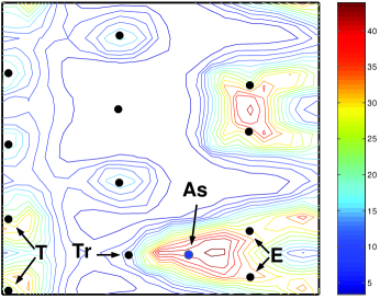
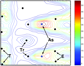
At this stage we have sound knowledge about the As adsorbed Si(211) surface at various coverages. In MCT growth experiments, better quality surfaces are obtained by adsorbing Te on the As-exposed Si(211) for the essential growth of MCT. Thus, it is important to investigate the atomic configuration of Te which forms the second layer on the Si(211). As-exposed Si(211) surfaces that we consider here are obtained by adsorbing As on Si(211). We consider only 1 ML As adsorbed Si(211) surface because recent X-Ray photoemission spectroscopy (XPS) data chad indicated that the As coverage on the Si(211) to be about 1 ML.
The 1 ML As adsorbed Si(211) surface (see Fig. 7) offers two distinct binding sites for Te. One is between two As atoms sitting on the trench Si atoms (denote as S1 site) and the other one is between the two terrace Si atoms (denote as S2 site). It is found that the energy gain in bringing a single Te atom from source and putting it at S1 is eV while that for S2 site is eV. Therefore, S1 site is more favorable at 1/8 ML coverage of Te. When a second Te atom is placed at another S1 site available on the surface in the presence of the first Te, the average energy gain for each Te is eV. Similarly when third and fourth Te atoms are placed at S2 sites available on the surface, the average energy gains are eV and eV respectively. Here we note that the energy gains are calculated by using the value of -3.16 eV for the bulk chemical potential of Te. Thus one would normally expect the Te coverage to be no less than 50% of 1 ML. However, in experiment, the Te coverage on the As-exposed Si(211) was found to be 20% - 30%. nibir . The discrepancy in the Te coverage suggests that the As adsorbed Si(211) may not be the most favorable surface. In other word, Te may not be adsorbing on the As-exposed Si(211) substrate that we have considered so far.
III.3 As Replaces Si on Si(211)
We have so far considered Te adsorption on As-exposed Si(211) surfaces that were obtained by adsorbing As on the bulk terminated Si(211). However, the Te coverage on such an As-exposed Si(211) with 1 ML of As does not agree with the experimental finding. nibir Borrowing from important results for Si(111) surface, bringans we investigate the possibility that Si atoms on the Si(211) surface may be replaced by As atoms. brill Here we report the results of total energy calculations for the possible replacement of Si(211) surface Si atoms by As. We consider an ideal Si(211) super-cell. As mentioned earlier, there are three kinds of atoms on the Si(211) which are named as terrace, trench and edge atoms. Replacement of one, two, four, and eight surface Si atoms by As atoms correspond to 1/8, 1/4, 1/2 and 1 ML coverage of As respectively. Separate calculations are carried out for the replacement of one, two and four terrace Si atoms by As. Similar calculations are done to replace trench and edge Si atoms by As respectively. Finally four terrace Si atoms along with four trench Si atoms are replaced to have 1 ML coverage of As on Si(211). The results are given below.
The net energy gain in the process of replacing one terrace Si atom by As is eV, one trench Si atom by As is eV and an edge Si atom by As is eV respectively. We notice that the replacement of a single trench Si atom by an As atom is the most favorable while replacement of terrace and edge atoms are equally less favorable. Comparing the energy gain due to the 1/8 ML of As adsorption on Si(211) with the energy gains in the replacement processes at 1/8 ML As coverage, we find that the replacement of any surface Si atom by As is energetically more favorable relative to the As adsorption.
The energy gain per As atom when two terrace Si atoms are replaced by two As atoms, two trench Si atoms are replaced by two As atoms and two edge Si atoms are replaced by two As atoms are 1 eV, 1.3 eV and 0.95 eV respectively. Here the replacement of trench Si atoms are most favorable while replacement of edge atoms are least favorable. When comparing with the adsorption of As at 1/4 ML coverage, we find that only the replacement of trench atoms are energetically more favorable.
We next replace four terrace Si atoms by As, four Si trench atoms by As and four edge Si atoms by As and corresponding energy gains per As atom are 1.01 eV, 1.3 eV and 0.92 eV respectively. Here also we find that the replacement of trench atoms are more favorable compared to the adsorption of As at 1/2 ML coverage.
An interesting and useful case is the replacement of eight Si atoms by eight As atoms which corresponds to 1 ML coverage of As because recent experimental data indicates chad that the As coverage on Si(211) is about 1 ML. Based upon the previous results, we replace four trench Si atoms along with four terrace Si atoms and we find that the average energy gain per Si replacement is 1.17 eV which is larger by 0.38 eV when compared with the adsorption of 1ML As on Si(211). We therefore, conclude that the replacement of Si atoms by As atoms are energetically more favorable compared to the adsorption. In other words, irrespective of As coverage, the As-exposed Si(211) surface obtained by replacing Si atoms with As is more favorable compared to that obtained by adsorbing As on Si(211). Thus, our results support the prevailing view brill that the Si atoms on Si(211) may be replaced by As atoms.
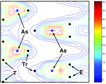
III.4 Te on As replaced Si(211)
It was mentioned earlier that Te is adsorbed on As-exposed Si(211) in the MCT growth experiment. The As-exposed Si(211) surface obtained by replacing all terrace and trench Si atoms of the bulk terminated Si(211) by As (corresponding to 1 ML As coverage) is considered here to study the Te adsorption. The As-exposed surface will have sites like G1, G2, G3 and G4 as discussed earlier. Based on our earlier results for the As adsorption on the bulk terminated Si(211) and also available dangling bonds on the As-exposed Si(211) surface, we conclude that a Te atom will prefer to bind at any of the four G sites available on the surface. An energy of 1.32 eV is gained when one Te atom is placed at G1 site. In presence of the first Te atom, the second Te is placed at the G3 site available on the surface of the super-cell (which corresponds to 1/4 ML coverage) and an average energy of 1.34 eV is gained for each Te atom. At this situation, two Te atoms at G1 and G3 sites make strong bonds with neighboring edge Si atoms and the edge Si atoms form dimers to lower the energy of the system. When the third Te is placed at G2 site in the presence of two Te atoms at G1 and G3 sites (which corresponds to 3/8 ML coverage) an average energy of 0.6 eV is gained for each Te. We see that the average energy gain for each Te atom is drastically reduced at 3/8 ML coverage of Te. This drastic drop in the average energy gain for each Te indicates that a transition takes place above 1/4 ML coverage. Though the average energy gain per Te indicates a kind of transition at 3/8 ML coverage of Te, it may not be give us a quantitative picture about the Te coverage on the As-exposed Si(211) because G1, G2, and G3 sites on the surface are no more identical in the presence of two Te atoms at G1 and G3 sites. We therefore, need to consider the energy gain for individual Te atoms as long as all bonding sites are not identical. First Te atom occupies the G1 site, bonds with two edge Si atoms and gain an energy of 1.3 eV. In presence of the first Te, the second Te occupies the G3 site, bonds with two other edge Si atoms and gains an energy 1.3 eV. The individual energy gains for first and second Te atoms are roughly same because Te atoms at G1 and G3 sites have similar surroundings. Note that at 1/4 ML coverage of Te (G1 and G3 sites in the super-cell are occupied by two Te atoms) dangling bonds of the edge Si atoms are completely saturated. This implies that the third Te atom can not bind to the surface unless it is capable of breaking the Si dimers that are formed at 1/4 ML coverage of Te. In fact our calculation reveals that the third Te atom placed at G2 site can not break the Si dimers. Furthermore, an energy comparison shows that we need to supply 0.8 eV of energy to bind the third Te atom on the As-exposed surface. This is the reason behind a drastic drop in average energy gain for each Te at 3/8 ML coverage of Te. Thus, 3/8 ML coverage of Te on the As-exposed surface is highly improbable. However, when two Te atoms are placed at G2 and G4 sites in presence of two Te atoms at G1 and G3 sites (which corresponds to 1/2 ML coverage), the Si(211) the edge Si dimers break to accommodate all four Te atoms. Under such circumstances, all four Te atoms bond equally strongly with the edge Si atoms. An average energy of 1.30 eV per Te atom is gained. Thus, it appears that Te coverage between 1/4 ML and 1/2 ML is improbable on the As-exposed Si(211). However, to have 1/2 ML coverage one has to go through coverages between 1/4 and 1/2 ML. Therefore, Te coverage beyond 1/4 ML (25 % of ML) is improbable and this result is in agreement with the experimental finding for the Te coverage nibir on the As-exposed Si(211).
IV Summary
Electronic structure calculations are performed to study the Te coverage on the As-exposed Si(211) surfaces. The As adsorption on Si(211) at 1/8, 1/4, 1/2 and 1 ML coverages are systematically studied. Then the Te adsorption study on the 1 ML As adsorbed Si(211) is done and it is found that 1/2 ML of Te adsorption is energetically feasible on the one ML As adsorbed Si(211) surface.
We have done another set of calculations to verify the prevailing idea that terrace and trench Si atoms on the Si(211) surface may be replaced by As. We found that replacement of any surface Si atoms by As atoms is energetically more favorable when compared with the adsorption of As on the Si(211) at 1/8 ML coverage. At 1/4 and 1/2 ML coverages the replacement of trench Si atoms by As are more favorable compared to the As adsorption on Si(211) while the replacement of edge atoms are least favorable. The As-exposed Si(211) with 1 ML of As is obtained by replacing all the trench and terrace atoms by As and it is found to be more favorable compared to that obtained by adsorbing 1 ML As on Si(211). The Te adsorption on such a favorable As-exposed Si(211) is investigated. A drastic drop in average energy gain per Te is noted at 3/8 ML coverage of Te. The drastic drop in the average energy gain suggests that the probable Te coverage on the As-exposed Si(211) is 25% of a ML which is confirmed by further analysis. This result agrees with the experimental finding. nibir
In conclusion, our results reveal that the replacement of surface Si atoms on Si(211) by As is energetically more favorable when compared with the As adsorption on Si(211). Thus our calculations support the prevailing view that the terrace and trench Si atoms on the Si(211) surface are replaced by As. The Te coverage on the As adsorbed Si(211) may be more than 50% of 1 ML which is way above the experimentally found value. However, the Te coverage on the energetically most favorable As-exposed Si(211)surface (surface terrace and trench Si atoms replaced by As) is found to be 25% of 1 ML and this is in agreement with the experimental finding. nibir
Acknowledgements.
This work was supported under the research agreement subcontract #S03-16 from the Electro-Optics Center (EOC), funded by the Marine Crops, monitored by Ray Balcerak and Kenneth Freyvogel under the direction of Karl Harris.References
- (1) Sillicon Surfaces and Formation of Interfaces by J. Dabrowski and H. -J. M ssig, World Scientific, Singapore (2000).
- (2) Introduction to Surface Thin Film Processes by J. A. Venables, Cambridge University Press (2000).
- (3) D. J. Chadi, Phys. Rev. B 29, 785 (1984).
- (4) B. Z. Olshanetsky and V. I. Mashanov, Surf. Sci. 111, 414 (1981).
- (5) N. K. Dhar, N. Goldsman, and C. E. C. Wood, Phys. Rev. B 61, 8256, (2000).
- (6) S. Rujirawat, L. A. Almeida, Y. P. Chen, S. Sivananthan and D. J. Smith, Appl. Phys. Lett. 71, 1810 (1997).
- (7) B. Yang, Y. Xin, S. Rujirawat, N. D. Browning and S. Sivananthan, J. Appl. Phys. 88, 115 (2000).
- (8) D. Smith, S. -C. Y. Tsen, D. Chandrasekhar, P. A. Crozier, S. Rujirawat, G. Brill, Y. P. Chen, R. Srorken, and S. Sivananthan, Materials Science & Engineering B 77 93 (2000).
- (9) Ph D thesis entitled The CdTe/Si(111):As interface by S. Rujirawat, University of Illinois at Chicago, USA (2000).
- (10) A. A. Baski and L. J. Whitman, Phys. Rev. Lett. 74 956 (1995).
- (11) A. A. Baski, S. C. Erwin, and L. J. Whitman, Surf. Sci., 392 69 (1997).
- (12) A. A. Baski, S. C. Erwin, and L. J. Whitman, Surf. Sci. Letters, 423 L265 (1999).
- (13) S. C. Erwin, A. A. Baski, L. J. Whitman and R. E. Rudd, Phys. Rev. Lett. 83, 1818 (1999).
- (14) J. N. Crain, J. L. McChesney, Fan Zheng, M. C. Gallagher, P. C. Snijders, M. Bissen, C. Gundelach, S. C. Erwin, and F. J. Himpsel, Phys. Rev B 69 125401 (2004).
- (15) S. L. Wright, H. Kroemer and M. Inada, J. Appl. Phys. 55, 2916 (1984).
- (16) T. Berghaus, A. Brodee, H. Neddermeyer and S. Tosch, Surf. Sci. 184, 273 (1987).
- (17) X. Wang and W. H. Weinberg, Surf. Sci. 314, 71 (1994).
- (18) R. Kaplan, Surf. Sci. 116, 104 (1982).
- (19) P. Sen, I. P. Batra, S. Sivananthan, C. H. Grein, N. K. Dhar and S. Ciraci, Phys. Rev. B 68 045314 (2003).
- (20) L. T. Romano, R. D. Bringans, X. Zhou, and W. P. Krik, Phys. Rev. B 52 11201 (1995).
- (21) C. Fulk et al. (Private Communication).
- (22) G. Brill, Y. Chen, N. K. Dhar and R. Singh, J. Electron. Mater., 32 717 (2003).
- (23) R. D. Bringans, Crit. Rev. Solid State Mater. Sci. 17 353 (1992).
- (24) N. K. Dhar, P. R. Boyd, M. Martinka, J. H. Dinan, L. A. Almeida, and N. Goldsman, J. Electron. mater., 29 748 (2000).
- (25) S. Mankefors, Surf. Sci. 443, 99 (1999).
- (26) D. Vanderbilt, Phys. Rev. B41, 7892 (1990); G. Kresse and J. Hafner, J. Phys.: Condens. Matter 6, 8245 (1994).
- (27) J. P. Perdew and Y. Wang, Phys. Rev. B46, 6671 (1992).
- (28) G. Kresse and J. Hafner, Phys. Rev. B47, R558 (1993); G. Kresse and J. Furtmüller. Phys. Rev. B54, 11169 (1996).
| Site: | B1 | D1 | G1 | V1 | M1 | F1 | H1 |
| BE (eV): | 4.66 | 4.35 | 5.64 | 5.28 | 5.12 | 5.43 | 4.04 |
| h (Å): | 1.86 | 1.69 | 0.73 | 0.58 | 0.84 | 0.61 | 1.60 |
| Site: | B1B2 | G1G3 | G1F3 | G1M3 | F1F3 |
|---|---|---|---|---|---|
| BE (eV): | 5.34 | 5.82 | 5.66 | 5.11 | 5.00 |
| h (Å): | 1.77 | 1.06 | 0.58 | 0.62 | 0.57 |
| Site: | B1B2B3B4 | G1G3M1M4 | G1G2G3G4 |
|---|---|---|---|
| BE (eV): | 5.35 | 5.72 | 5.80 |
| h (Å): | 2.10 | 0.96 | 0.32 |