Fabrication and characterization of scanning tunneling microscopy superconducting Nb tips having highly enhanced critical fields
Abstract
We report a simple method for the fabrication of Niobium superconducting (SC) tips for scanning tunnelling microscopy which allow atomic resolution. The tips, formed in-situ by the mechanical breaking of a niobium wire, reveal a clear SC gap of 1.5 meV and a critical temperature Tc = 9.20.3 K, as deduced from Superconductor Insulator Normal metal (NIS) and Superconductor Insulator Superconductor (SIS) spectra. These match the values of bulk Nb samples. We systematically find an enhanced value of the critical magnetic field in which superconductivity in the tip is destroyed (around 1 T for some tips) up to five times larger than the critical field of bulk Nb (0.21 T). Such enhancement is attributed to a size effect at the tip apex.
keywords:
Scanning tunnelling microscopy , superconducting tip , critical fieldPACS:
68.37.Ef , 74.25.Op , 74.50+r , 74.78.Nd, , , , , and
1 Introduction
Among the variety of surface techniques, Scanning tunneling microscopy and spectroscopy (STM STS) has a special role in the investigation of surface topography and local electronic properties on the atomic scale [1]. The device is based on the precise measurement of the vacuum tunneling current between an atomically sharp tip and a sample as a function of the applied voltage. The magnitude of the current depends on the tip sample distance and on the density of electronic states of both the tip and the sample. Usually the STM tip is made of a normal metal in which the density of electronic states (DOS) near the Fermi level can be considered, in a first approximation, constant. Thus the measured current as a function of tip position reflects changes in either the sample DOS or the topography.
Meservey[2] had suggested the use of an SC material for the fabrication of the STM tip. One advantage of an SC tip is the enhanced spectroscopic resolution due to the singularity in the SC DOS at the gap edge. This reduces significantly the thermal smearing, due to the Fermi-Dirac distribution, in comparison to the case of a normal metal tip. Of major interest, an SC tip with an SC sample allows, in principle, direct cooper pair tunneling (Josephson current[3]), which is well known in point contact and planar SIS junctions[4]. In the investigation of local electronic properties of superconductors, the STM is almost exclusively used with a normal tip, thus exploiting single electron processes, resulting in the well known BCS tunneling DOS. The gap function is inferred from the spectrum but does not indicate directly the existence of a condensate. With an SC tip on the other hand the appearance of a Josephson current is a definite signature of a coherent state.
In general a proper STM tip has to be sharp enough to allow for good spatial resolution (in the best case atomic resolution). From a theoretical point of view it was questioned whether an atomically sharp tip would still show SC properties. One certainly expects that the geometry and dimensions of the tip could have an effect on it’s properties as, for example, in the case of an applied magnetic field. Additionally, one must avoid the oxidation of the surface layer of the tip, which for normal metals is easily achieved, for example, by mechanically cutting a PtIr wire in air. For an SC tip this is not so trivial: SC elements from which tips can be formed like Al, Nb and Pb oxidize rapidly. Other materials, such as high temperature superconductors, suffer from surface degradation and the difficulty in controlling the geometry, due to their complex structure and composition.
Pan and Hudson[5] have shown that atomic resolution and superconductivity can be obtained at the same time. They have used a mechanically cut Nb wire to obtain a sharp tip and further apply a voltage pulse between the tip and an Au target inside the STM vacuum chamber. This removes the oxide and further sharpens the tip. The tips were indeed superconducting and allowed for atomic resolution; however, the measured gap values varied from one tip to the other, ranging from a few tenths of a meV and up to 1.5 meV. The authors suggest that the superconductivity measured at the end of the tip is in fact due to a proximity effect induced by the bulk. In such a scenario, the amplitude of the measured gap can vary due to changes in tip apex geometry and composition. The latter are claimed to be a result of the voltage pulse application.
Naaman et al.[6]have used a two layer deposition method in which a Å layer of Pb is deposited on a mechanically cut PtIr tip and then covered by a Å layer of Ag. In this method, the Ag layer serves as a protection against the oxidation of the lead. The superconductivity of the tip is based on the proximity effect and a gap is induced in the Ag layer. Finally Suderow et al.[7] have used a method in which the STM tip is successively driven into and pulled out of a Pb layer and results in the formation of a Pb tip. As the process is done inside a vacuum chamber and at a temperature of K, the resulting tip is mechanically stable and does not oxidize.
The last two methods are inferior to the first one, as they use Pb which has a lower critical temperature and gap value ( K ; meV) in comparison to Nb, being the element with the highest critical temperature (K; meV). This limits the temperature range in which the tip can be used and enlarges the effect of thermal fluctuations on the measured Josephson current [15]. Giubileo et al.[8] have used a MgB2 grain glued to a PtIr tip as a STM tip, this technique allowed obtaining atomic resolution and has the advantage of a high critical temperature ( 39K) and a relatively large SC gap ( meV). However spatial resolution is not easily reproduced in tips of this kind and the non trivial two band effects in MgB2[8] hinder the interpretation of the measured conductance spectra.
Here we propose a new and simple method for the preparation of SC Nb STM tips which does not require a voltage pulse application. The method is based on mechanically cutting an Nb wire inside the STM’s vacuum chamber (a similar method was used to create a ferromagnetic tip by Koltun et al.[9]). The resulting Nb tips allow obtaining atomic resolution topographic images and have a reproducibly measured gap value of meV which matches the value obtained for bulk Nb samples. By following the temperature dependence of the conductance spectra measured using an Nb tip and an Au sample we found the SC gap to close at a temperature of K which coincides with the critical temperature of bulk Nb samples. A clear deviation from the bulk properties is observed under the application of magnetic field. All tips exhibit a strongly enhanced value of the critical field with a maximum measured value of T, times larger than the bulk value of T. We explain this enhancement as a result of the confinement of the superconducting phase by the magnetic field to a nano-metric region at the tip apex.
2 Tip preparation and Samples
The tips are made from a niobium wire of mm diameter from which we cut a cm piece. Using a surgical knife we then create a thin groove around the wire thus creating a weak point. Following, one end of the wire is glued using an ultra high vacuum compatible conducting silver epoxy to a tip holder and the other end is tied to create a loop as shown in figure 1a. The tip and tip holder are then put into an autoclave oven for a 1 hour baking of the glue at a temperature of C. The final cutting of the tip is done inside the vacuum chamber which contains the home-made low temperature (4.2K) STM at a vacuum of mbar and at ambient temperature. The cutting process is done using a mechanical manipulator which allows us to first place the loop around a metallic pin and subsequently to pull the tip holder. This stretches the Nb wire until it breaks at the designated weak point thus creating the tip (see fig 1b). We then install the tip in the STM head, perform the coarse approach and lower the microscope to the bottom of a cold finger where, owing to cryo-pumping, the vacuum is much better than in the upper part of the chamber. This entire process from the moment the tip is cut lasts around minutes and is short enough to avoid the creation of an oxide layer on the tip apex. Longer preparation times, or poorer vacuum conditions, increase the number of tips showing insulating behavior at low temperature, indicating the formation of an oxide layer at the tip apex. Under proper conditions, roughly percent of the tips show superconducting properties at low temperatures.

To characterize the tip properties we have used three kinds of samples: Au samples of Å in thicknesses deposited on Mica substrates by thermal evaporation (for preparation conditions see[10]), NbSe2 cleaved in the vacuum chamber and a thermally evaporated Nb/Pd sandwich sample deposited on a Si substrate covered by a Å SiO buffer layer. In the last sample, a thick Nb layer (400 Å) was covered by a thin Pd ( Å) layer to protect the Nb from oxidizing and to allow a proximity induced gap with an amplitude close to that of bulk Nb to appear in the Pd layer.
3 Experimental Results
In order to check the spatial resolution of our Nb tip, we made topographic scans of an in-situ cleaved NbSe2 sample. A current image scan of 165 Å 165Å measured at a temperature of K is shown in Figure 2 which clearly shows the atomic lattice of the surface. This confirms that indeed the Nb tip is atomically sharp.

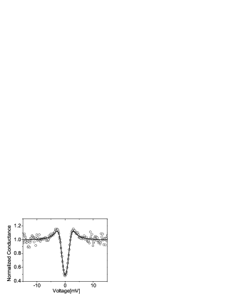
Figure 3 shows a typical NIS conductance curve measured using an Nb tip and an Au sample at a temperature of K. The conductance spectra were obtained by numerically differentiating the measured I,V curves which were obtained by applying a digital voltage ramp and measuring the current. In general the spectra are symmetric with respect to zero bias representing the symmetry of the BCS DOS with respect to energy. The depression in the conductance near zero voltage due to the SC gap is clearly visible and is followed, at higher voltage, by clear peaks as expected for the BCS DOS. The additional oscillations visible at even higher voltages are not symmetric with respect to zero voltage and are due to experimental noise. The measured spectrum is fitted using the BCS DOS with an addition of a life-time broadening parameter [11]. The best fit is given using a gap value of meV which matches the value measured for bulk Nb and a broadening parameter meV. The broadening parameter accounts for both experimental broadening, resulting from bias jitter, and inelastic scattering or pair breaking processes.
We find the gap value to be reproducible in different positions on the same sample and using several Nb tips and Au samples, while the value of the broadening parameter changes between meV.
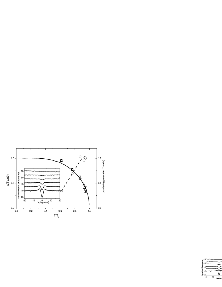
Figure 4 shows the values of the BCS fit parameters, the normalized order parameter and the life-time broadening parameter as a function of the normalized temperature, , where we have used meV and K. The solid line depicts the theoretical temperature dependence according to the BCS theory and is in agreement with the values extracted from the experimentally measured spectra. The inset shows the measured conductance spectra and the theoretical fit in the range of 5.8 K to 9.5 K. One clearly observes the closing of the SC gap as the temperature is increased. At K a gap is still visible while at K a flat conductance curve is measured, indicating a transition of the tip to the normal state at K. This temperature is in agreement with the one measured for bulk Nb samples, K and with the value used for creating the normalized temperature curve ( K). The life-time broadening parameter is found to increase with temperature (circles in fig 4), starting from 0.34 meV at T=5.8K and saturating at around 1meV as we approach . Naaman et al. [6] reported on an increase in the broadening parameter for their Pb tips with meV at 2 K and rising up to meV at T=6 K. As our pre-amplifier is located on the microscope, and thus is subject to roughly the same temperature changes as the junction, we expect our bias jitter to increase with temperature due to increased fluctuations in the amplifier’s virtual ground. Therefore it is impossible at this stage to determine if the increase in the value of has also an intrinsic source, such as a rise in the pair breaking rate near the tip apex as a function of temperature.
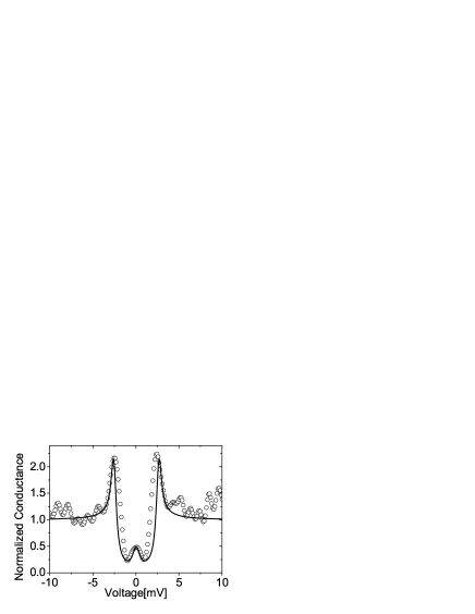
In order to verify that indeed the use of a SC tip enhances the spectral features measured on a SC sample we have used an Nb/Pd (2000 Å/50 Å) sandwich type sample, in which superconductivity is induced in the thin Pd layer by the thick Nb layer due to the proximity effect. The covering Pd layer protects the Nb layer from oxidizing which is necessary since the sample was grown in a different vacuum system than the one used for the STM measurements. Figure 5 shows the spectra measured at a temperature of 6.6K. At this temperature, a zero-bias peak in the conductance is clearly observed. This peak is typical for SIS junctions at finite temperature and is the result of the enhanced tunnelling probability of thermally excited quasi particles. Additionally, the amplitude of the gap-edge peaks is considerably enhanced in comparison to the NIS case (fig 3) and the normalized conductance value reaches a minimum value of much lower than the one obtained for the NIS case . The oscillations observed at voltages above the gap are due to experimental noise. The best fit of the data is shown in the figure (solid line) and the fit parameters ( meV, meV) confirm that indeed both electrodes are SC. The reduced gap value in Nb/Pd in comparison to that of the Nb tip is reasonable as it is induced by the proximity effect while the Nb gap for the tip fits the value expected at T=6.6K.
4 Magnetic Field
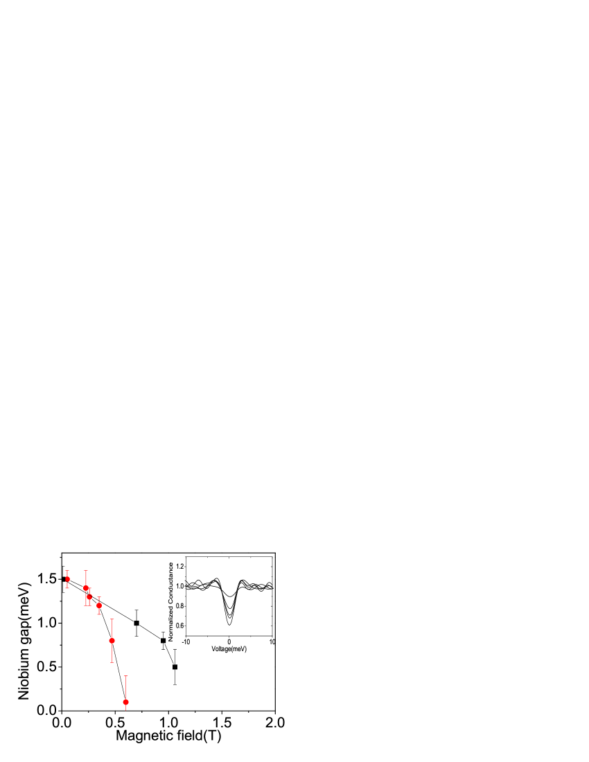
In order to check the magnetic field response of our Nb tip we have studied the NIS configuration using an Nb tip and an Au sample. We then applied a magnetic field parallel to the Nb wire whose apex forms the tip. Starting from zero field we have measured the tunneling conductance as a function of field up to 1.5 T. A typical result is shown in the inset of figure 6. The data shown is Fourier filtered to remove the high frequency noise appearing in our system due to the effect of the magnetic field on the pre-amplifier. As the field was increased we observed a closing of the gap, however even at fields higher than the second critical field of bulk Nb ( T at K) a non-zero gap could be clearly observed. We note the lowest field in which we found no evidence for a gap in the spectra as Hctip. The values of Hctip, all obtained at K, varied from one tip to the other in the range of T to T, but were always considerably enhanced in comparison to the value measured in bulk samples. As our measurements were made at K, the actual values of the critical field at zero temperature should be even higher.
The enhancement of the critical field is clearly seen in figure 6 where we present the value of the SC order parameter as a function of magnetic field, obtained by fitting the measured curves using the BCS formula, for two of our tips. We consider this enhancement to be a result of the special geometry of the tip. Far from its apex the tip has the properties of a bulk sample thus becoming normal when the applied field exceeds the value of the bulk one. However as the tip narrows towards its apex the mean free path and consequently the effective coherence length become limited and are reduced in comparison to their bulk values, thus an enhancement of the critical field similar to that calculated for thin films in the dirty limit [12] is expected. We note that in such a case the field dependence of the gap is expected to be quadratic, in agreement with our experimental results. Misko et al. have theoretically studied the field dependence of a superconductor with a multi conoid geometry by solving the Ginzburg Landau equations [13]. Indeed they have found an enhancement of towards the apex of the cone. The model was solved numerically for the case of Pb, taking nm and nm (set by the width of the bridge) and showed an enhancement of by a factor of . Experimentally this enhancement was observed in a Pb nano-bridge formed between an STM tip an a Pb sample by Rodrigo et al.[14] The predicted enhancement fits well with our maximal measured value of T. The results should be applicable also to Nb as nm and the difference in coherence length ( nm, nm) becomes irrelevant as the width of the confinement region is much smaller than both.
Within the above model one can account for the different values of found experimentally in different tips as a result of variations in the tips geometries. Moreover, the zero field spectra of the two tips are almost identical in contrast to their field dependencies, as indicated in fig.6, which exhibit values differing by at least percent. This perfectly fits with the model, since the zero field conductance should not be effected by the tip geometry.
5 Conclusions
To conclude we have developed a simple method for the fabrication of superconducting Nb tips suitable for atomic resolution STM. The tunneling spectra show a gap value and a critical temperature matching the values found in bulk Nb samples but a highly enhanced value of the critical field, up to 5 times larger. The tips exhibit the expected enhancement of the STM spectroscopic resolution in the SIS configuration. Future prospects could include measurements of Josephson currents as a function of position, i.e. a Josephson STM. Using the theoretical condition for the measurement of Josephson currents, [15], where is the quantum resistance, yields for Nb : , which at this point could not be obtained due to limitations in our present experimental setup.
6 Acknowledgements
The authors would like to thank Tristan Cren for fruitful discussions. One of the authors, A.K. would like to thank R.B. Beck and O. Naamam for their advice.
References
- [1] G. Binning, H. Rohrer Phys. Rev. Lett 49, 57 (1982)
- [2] R. Meservey Phys. Scr. 38 272 (1988)
- [3] B.D. Josephson Phys. Lett. 1, 251 (1962)
- [4] R.C. Jaklevic, J. Lambe, J.E. Mercereau, A.H. Silver Phys. Rev. 140, A 1628 (1965)
- [5] S. H. Pan, E. W. Hudson and J. C. Davis, Appl. Phys. Lett., 73, 2992 (1998)
- [6] O. Naaman,W. Teizer, and R. C. Dynes, Rev. Sci. Instrum. 72, 1688 (2001)
- [7] H. Suderow, M. Crespo, P. Martinez-Samper, J. G. Rodrigo, G. Rubio-Bollinger, S. Vieira, N. Luchier, J.P. Brison, P.C. Canfield, Physica C 369, 106, (2002)
- [8] F. Giubileo et al. Phys. Rev Lett. 87 177008 (2001)
- [9] R. Koltun, M. Herrmann, G. Güntherodt, V.A.M. Brabers., Appl. Phys. A 73, 49 (2001)
- [10] J.A. De Rose, T. Thundat, LA Nagahara, SM Lindsay Surf. Sci. 256, 102 (1991)
- [11] R. C. Dynes, V. Narayanamurti and J. P. Garno Phys. Rev. Lett. 41, 1509 (1978) (1966)
- [12] M. Tinkham, Introduction to Superconductivity McGraw-Hill, Inc(1996)
- [13] V.R. Misko, V.M. Fomin and J.T. Devreese Phys. Rev. B. 64 014517 (2001)
- [14] J. G. Rodrigo, H. Suderow, and S. Vieira Phys. Stat. Sol. 237 386 (2003)
- [15] J. Smakov, I. Martin and A. V. Balatsky Phys. Rev. B. 64, 212506 (2001)