Time-resolved broadband analysis of slow-light propagation and superluminal transmission of electromagnetic waves in three-dimensional photonic crystals
Abstract
A time-resolved analysis of the amplitude and phase of THz pulses propagating through three-dimensional photonic crystals is presented. Single-cycle pulses of THz radiation allow measurements over a wide frequency range, spanning more than an octave below, at and above the bandgap of strongly dispersive photonic crystals. Transmission data provide evidence for slow group velocities at the photonic band edges and for superluminal transmission at frequencies in the gap. Our experimental results are in good agreement with finite-difference-time-domain simulations.
pacs:
42.70.Qs, 78.47.+p, 41.20.Jb, 42.30.RxI Introduction
Electromagnetic waves propagate in straight trajectories in homogeneous materials. This simple propagation changes when the wave encounters inhomogeneities and is scattered. Interference of the scattered waves can modify significantly their propagation. The careful engineering of the inhomogeneities may lead to the inhibition of the propagation in certain directions and to the enhancement in others. It is also possible to speed-up Steinber:93 ; Spielmann:94 ; Longhi:01 ; Hache:02 ; Munday:02 ; Solli:03 ; Galli:04 or slow-down Tarhan:95 ; Imhof:99 ; Vlasov:99 ; Bayindir:00 ; Notomi:01 ; Galli:04 the propagation of the wave and even to localize it Wiersma:97 . The full control of the propagation of electromagnetic waves is intensively pursued since this control will lead to new concepts in numerous fields such as information processing Noda:03 , laser physics Painter:99 , bio-sensing Alivisatos:04 and quantum optics Lodahl:04 .
One of the most prominent candidates for the control of the propagation of electromagnetic waves are photonic crystals. Photonic crystals are periodic structures of two or more materials with different refractive indices Yablonovitch:87 ; John:87 . Interference of waves scattered at different lattice planes of the crystal determine its optical properties. Depending on the structure and if the scattering is strong enough a photonic band gap (PBG) might be created. A PBG is a frequency range in which no optical modes are allowed and, consequently, the propagation of waves in this range is forbidden. Particulary attractive is the extraordinary optical dispersion that photonic crystals exhibit, which leads to a pronounced variation of the wave’s group velocity. The resonant scattering at the band edges of the gap gives rises to a strong reduction of the group velocity and a significant group velocity dispersion Imhof:99 . This slow propagation, which increases the interaction time between the wave and the crystal, constitutes the basis for the development of sensors for gases and bio-molecules Alivisatos:04 and more sensitive non-linear components Soljacic:04 . A wave with a frequency in the PBG incident on a photonic crystal is reflected. However, if the crystal has a finite thickness, a fraction of the wave’s intensity is transmitted. While the transmitted intensity decreases exponentially with the crystal thickness, the transmission time is independent of this thickness, which may lead to superluminal transmission. Tunneling processes through photonic structures are of great scientific and technological interest Chiao:97 ; Nimtz:03 ; Stenner:03 ; Nimtz:04 . Among the reasons driving this interest are the similarities with the tunneling of quantum particles and the ongoing intense discussions on the propagation in the superluminal regime Stenner:03 ; Nimtz:04 .
In spite of the fundamental and technological relevance of dynamic properties of electromagnetic waves in photonic crystals most of the investigations so far focus only on stationary measurements. This focus is mainly imposed by the complexity of phase sensitive techniques at high frequencies. Reports on the group velocity of waves in optical photonic crystals are thus seldom and limited to narrow frequency ranges Munday:02 , to weakly scattering photonic crystals Tarhan:95 ; Imhof:99 ; Vlasov:99 ; Longhi:01 , or to low dimensional photonic structures Steinber:93 ; Spielmann:94 ; Longhi:01 ; Hache:02 ; Solli:03 ; Galli:04 .
In this article we present a broadband time domain investigation of the propagation of electromagnetic waves in strongly-scattering-three-dimensional photonic crystals of variable size. In our investigation we use terahertz time-domain spectroscopy, a technique capable to generate ultrashort broadband pulses of THz radiation and to detect the amplitude and the phase of these pulses. Through the direct access of amplitude and phase an unprecedented precision in the analysis of the propagation of electromagnetic waves in photonic crystals is achieved. The extinction coefficient is obtained from the exponential decrease of the transmitted amplitude with the thickness of the crystal. From the phase analysis of the transmitted wave the wave number, the effective refractive index and the group velocity are derived. Very strong dispersion at the edges of the gap and anomalous dispersion at frequencies in the gap are observed. Even in a photonic crystal with a thickness of only four unit cells the group velocity is dramatically reduced at the band edges by almost a factor 15 with respect to the speed of light in vacuum, while anomalous dispersion in the gap gives rise to superluminal transmission.
II Samples
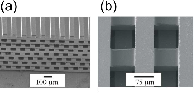
The photonic crystals investigated are formed by intrinsic silicon and air. Intrinsic silicon has a very large refractive index , and virtually no absorption at terahertz frequencies. Photonic crystals are fabricated by micromachining thin wafers of silicon, and piling them to form a layer-by-layer structure Chelnokov:97 ; Gonzalo:02 . Such a structure consists of a transverse stacking of arrays of dielectric rods with a face-centered-tetragonal lattice symmetry Ho:94 ; Sozuer:94 . This type of crystal structure exhibits a very large photonic band gap Ho:94 . The micromachining of our crystal was done with a programmable dicing saw, as described in more detail in Ref. Gonzalo:02 : parallel grooves spaced by were diced on one side of a wafer with a thickness of . The thickness of the grooves is and the depth one half of the thickness of the wafer, i.e., . Perpendicular grooves to these with the same thickness and depth were diced in the opposite side. This method produces a square grid of apertures. To form the photonic crystal structure several of these grids are piled. Consecutive grids are shifted by one half of the period and two of them form a single unit cell in the stacking direction. The dimension of this unit cell is thus . The calculation of the band structure of this specific photonic crystal predicts a PBG centered at 0.5 THz. Figures 1(a) and (b) are scanning electron microscope images of a layer-by-layer structure with a thickness of 4 unit cells. Figure 1(a) is a side view of the structure along the stacking direction, while (b) is a top view of the same photonic crystal.
III Terahertz transmission through photonic crystals
III.1 experimental setup
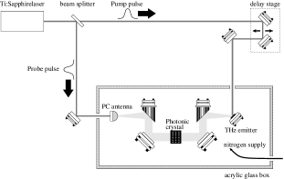
For the experiments we use a THz time-domain spectrometer Exter:90 . This setup is schematically depicted in Fig. 2. A train of femtosecond pulses from a Ti:sapphire laser is split to generate and detect single-cycle terahertz pulses. One beam, the so-called pump beam, is incident on an InGaAs surface field emitter, generating THz radiation. The THz pulses are collected and collimated by a parabolic mirror placed at the focal distance to the emitter. This THz beam is incident normal to the surface of the crystal, and the transmitted amplitude is focused with a parabolic mirror onto a photoconductive antenna. The antenna is gated with the pulses from the second beam of the Ti:sapphire laser. By means of a computer controlled delay stage, the length difference between the generation and detection optical paths is varied and the THz field amplitude is detected as a function of time with sub-picosecond time resolution. Water vapor absorbs THz radiation, therefore, the THz setup is enclosed in a box which is continuously fluxed with nitrogen gas.
Even though the measurements were done at only one direction, it has been demonstrated by Imhof et al. that 1D models are not able to explain the measurements of the group velocity near the band edges of 3D photonic crystals Imhof:99 .
III.2 Transmission measurements
We have measured the transmission of THz pulses through photonic crystals with different thickness ranging from 1 to 4 unit cells. The experimental transients of the transmitted field amplitude are plotted in Fig. 3(a). The reference pulse, i.e., the setup response, is also plotted in the same figure.
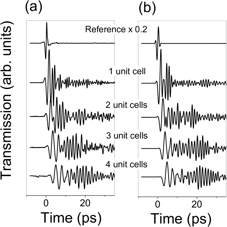
The measurements are compared with numerical simulations using the finite-difference-time-domain FDTD method. These simulations are plotted in Fig. 3(b), and were performed with a commercial software (FullWave by RSoft). The spatial resolution of the simulations is 3 and the temporal resolution is 5 fs. The incident field was approximated to a plane wave by using a Gaussian field distribution with a width much larger than the size of the simulation region. The temporal shape of the input THz field was a single-cycle pulse, with a center wavelength of 500 . The transmitted field was calculated at a distance of 2.3 mm from the source.
As can be seen in Fig. 3, the transmitted pulse experiences a significant dispersion growing with the thickness of the crystal. Signatures of the PBG formation become directly visible in the time domain data. Particulary in the thickest crystals, low frequencies, belonging to the lower photonic crystal band, and high frequencies, associated to higher bands, are separated in time domain.
To analyze the transmission we calculate the complex Fourier transform of the time-domain transmission through the crystal and normalized it by the reference measured without the sample. This transformation leads to a transmission of the form
| (1) |
The modulus is the spectrally resolved field transmission coefficient, and the argument is the phase difference between the transmission through the crystal and the reference. Equation (1) can be written as
| (2) |
where is an effective propagation constant for the transmission through the crystal and is the thickness of the crystal. The effective propagation constant is given by
| (3) |
where is the effective refractive index and the extinction coefficient of the crystal. The transmission is thus proportional to
| (4) |
The amplitude transmitted through the crystal decreases exponentially with the crystal thickness
| (5) |
while the phase difference is given by
| (6) |
It is important to mention that the transmission is measured outside the photonic crystal. Therefore the propagation constant has a real component or wave number even at frequencies within the gap. In section III.3 the analysis of the phase and the dispersion of the photonic crystals are discussed in detail.
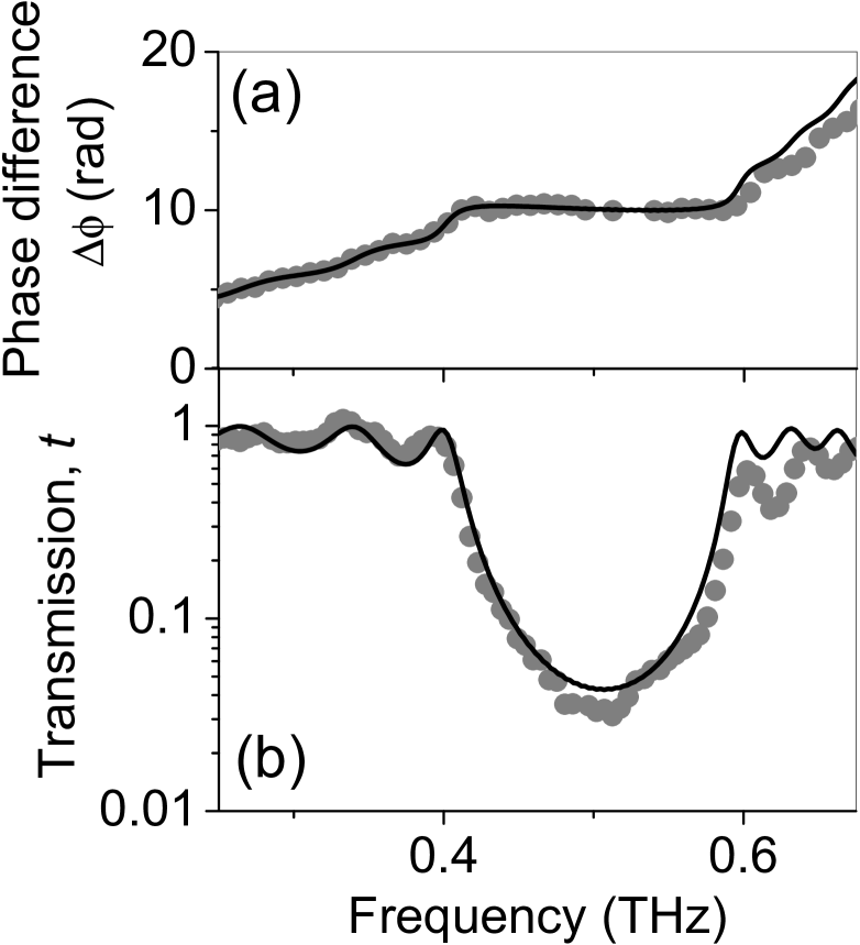
The amplitude transmission coefficient and the phase difference of a photonic crystal with a thickness of 3 unit cells are plotted in Fig. 4. The circles in this figure correspond to the measurements and the solid lines are results of the FDTD simulation. All the crystal parameters in the simulation, i.e., structure, dimensions and refractive index, are known, and the remarkably good agreement between simulation and measurement is obtained without adjusting any parameter. The transmission (Fig. 4(b)) drops strongly in the frequency range defined by the gap, i.e., 0.4-0.6 THz. At these frequencies the phase difference (Fig. 4(a)) is nearly constant. The interference pattern that is apparent by the oscillations in the transmission at low and high frequencies are Fabry-Perot resonances due to multiple reflections at the crystal interfaces.
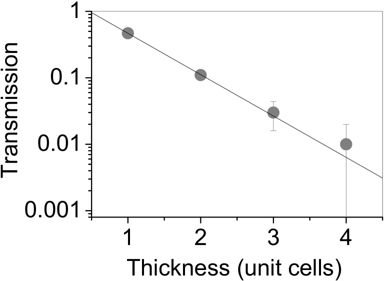
The extinction coefficient describes the attenuation of the wave amplitude as it propagates through the medium. In photonic crystals made of non-absorbing constituents, such as those investigated here, the extinction of the transmitted amplitude at frequencies within the gap is due to destructive interference of multiply scattered waves. At these frequencies the wave is Bragg reflected and only a small fraction is transmitted through the crystal. According to Eq.(5) the amplitude decreases exponentially with the crystal thickness and with an attenuation length . This attenuation length is a direct measure of the photonic strength of the crystal. Weakly scattering photonic crystals have attenuation lengths of the order of tens of unit cells, while in strongly scattering crystals is on the order of a few unit cells.
Figure 5 depicts the minimum transmission centered at the gap frequency of 0.5 THz as a function of the thickness of the crystal. The line in Fig. 5 is an exponential fit to the measurements from which we obtain an amplitude attenuation length of . This attenuation length is even smaller than one unit cell ( times the lattice constant), indicating an extraordinarily strong scattering in Si layer-by-layer structures Ozbay:96 ; Lin:98 .
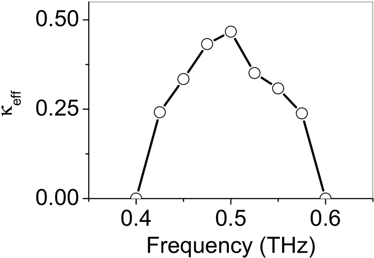
The extinction coefficient is represented in Fig. 6 for different frequencies. Radiation with a frequency outside the gap can propagate through the crystal being only weakly reflected at the interfaces. For these frequencies we have . At frequencies within the gap the transmitted amplitude decreases exponentially with leading to a positive . The largest value of , or equivalently the smallest , is at the central frequency of the gap.
III.3 Phase analysis
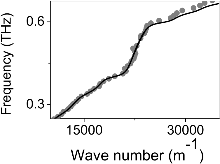
The dispersion properties of the electromagnetic wave propagating through the crystal were obtained as described in Refs. Robertson:92 ; Ozbay:94 and in the previous section. The measured phase difference between the transmission through the photonic crystal and the reference was used to calculate the wave number
| (7) |
where is the thickness of the photonic crystal, is the speed of light in vacuum and the angular frequency. The measured wave number of a layer-by-layer structure of 3 unit cells is shown in Fig. 7 with circles. The solid line in this figure represents the data from the FDTD simulations. The difference between measurement and simulation at high frequencies can be ascribed to small imperfections and misalignments in the structure.
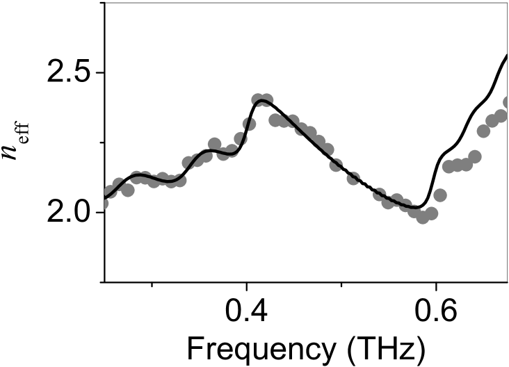
The effective refractive index of the crystal , defined as , is plotted in Fig. 8 versus the frequency. The FDTD simulation is represented in the same figure with a solid line. There is a distinct increase of at the low frequency band edge, i.e., 0.4 THz, followed by a remarkable decrease in the gap. At the high frequency band edge, i.e., 0.6 THz, rises again. As we are going to see, the increase of the effective refractive index at the band edges gives rise to a strong reduction of the group velocity, while the anomalous dispersion in the gap leads to superluminal transmission.
To calculate the group velocity , we use the standard definition , where is the group time delay. With the expressions of and , the effective group velocity can be written in the familiar form Jackson
| (8) |
The dispersion in introduced by the photonic crystal is described by the second term of the denominator, i.e., the derivative of with respect to the frequency.
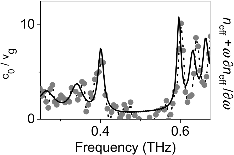
The inverse of the group velocity multiplied by , i.e., the denominator of Eq. 8, is plotted in Fig. 9 with circles, and the corresponding FDTD simulation with a solid line. The large dispersion at the band edges due to the resonant scattering gives rise to a strong reduction of the group velocity. The oscillations of the group velocity at low and high frequencies that are clearly visible in the simulation are due to the multiple reflections at the crystal interfaces. The anomalous dispersion at frequencies in the gap, which is characterized by the negative value of , increases the group velocity as defined by Eq. 8. If the crystal is thick enough this group velocity may be larger than the speed of light in vacuum. This result can be appreciated in Fig. 9, where the average value of in the gap of a crystal with a thickness of only 3 unit cells is .
Although the analysis presented above is the most accurate for the study of the dispersion characteristics of photonic structures, time-frequency representation methods are more intuitive and might be useful in this study Capus:03 . As an example of these methods, we plot in Fig. 10 the short time Fourier transform STFT Gamble:99 of the transmission through the photonic crystal with a thickness of 2 unit cells. The STFT is calculated by applying a window or a band pass filter to the time domain signal and Fourier transforming the signal within this window to obtain the spectral contain for a certain time delay. The process is repeated by shifting the time window over the entire time interval of the measurement. In this way temporal and spectral information are simultaneously retrieved. The contour plot of Fig. 10(a) is the transmitted amplitude through the photonic crystal, where the blue stands for no transmission and red for high transmission, as a function of time and frequency, calculated with a Hanning time window 8 ps wide. The THz transients are plotted in Fig. 10(b), where the red curve is the transmission through the crystal and the blue line corresponds to the reference. The amplitude transmission coefficient is plotted in Fig. 10(c). Consistently with the phase analysis, the time delay is the largest at the band edges, where the group velocity reaches its minimum value. At frequencies within the gap the transmission decreases significantly and the time delay becomes smaller.
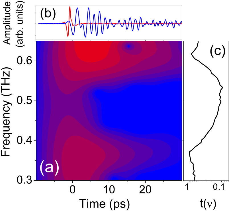
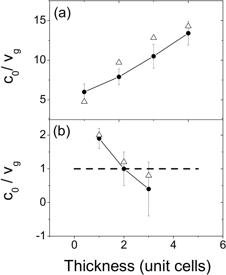
Figure 11 summarizes the salient features of the group velocity and presents its dependence on the thickness of the crystal. Fig. 11 (a) displays the inverse of multiplied by at the high frequency band edge, and (b) represents the average value of in the gap. The circles in these figures correspond to the measurements, while the open triangles to the FDTD simulations. The group velocity at the band edge is rapidly reduced as the thickness of the crystal increases. With only four unit cells this group velocity is almost a factor 15 slower than the speed of light in vacuum. On the other hand, the group velocity in the gap rapidly increases as the thickness of the crystal is augmented. For a photonic crystal of 3 unit cells the group velocity is roughly two times larger than the speed of light in vacuum. The transmission at gap frequencies of the thickest photonic crystal was lower than the noise level of our setup. For an infinite and defect-free photonic crystal one should expect a zero group velocity at the band edges and a no transmission in the gap.
IV summary
Through the direct access of amplitude and phase, terahertz time-domain spectroscopy offers unprecedented possibilities for the fundamental study of the propagation of electromagnetic waves in photonic structures. We have investigated the propagation of single-cycle THz pulses through strongly scattering photonic crystals with different thickness over a large bandwidth covering more than an octave below, at and above the bandgap. At frequencies within the gap we observe an attenuation length smaller than one unit cell and anomalous dispersion. The strong dispersion introduced by the crystal gives rise to extremely low group velocities at the band edges and to superluminal transmission in the gap.
acknowledgements
We gratefully acknowledge the assistance of C. Schotsch and K. Berdel with the fabrication and characterization of the photonic crystals. We are indebted with A. Stahl for fruitful discussions and with F. Merget and O. Winkler for the scanning electron microscope photographs. We acknowledge financial support by the European Commission under the project Interaction.
References
- (1) A.M. Steinberg, P.G. Kwiat, and R.Y. Chiao, Phys. Rev. Lett. 71, 708 (1993).
- (2) Ch. Spielmann, R. Szipöcs, A. Stingl, and F. Krausz, Phys. Rev. Lett. 73, 2308 (1994).
- (3) S. Longhi, M. Marano, P. Laporta, and M. Belmonte, Phys. Rev. E 64, 055602(R) (2001).
- (4) A. Haché and L. Poirier, Appl. Phys. Lett. 80, 518 (2002).
- (5) J.N. Munday and W.M. Robertson, Appl. Phys. Lett. 81, 2127 (2002).
- (6) D.R. Solli, C.F. McCormick, C. Ropers, J.J. Morehead, R.Y. Chiao, and J.M. Hickmann, Phys. Rev. Lett. 91, 143906 (2003).
- (7) M. Galli, B. Bajoni, F. Marabelli, L.C. Andreadi, L. Pavesi, and G. Pucker, Phys. Rev. B 69, 115107 (2004).
- (8) İ.İ. Tarhan, M.P. Zinkin, and G.H. Watson, Opt. Lett. 20, 1571 (1995).
- (9) A. Imhof, W.L. Vos, R. Sprik, and A. Lagendijk, Phys. Rev. Lett. 83, 2942 (1999).
- (10) Y.A. Vlasov, S. Petit, G. Klein, B. Hönerlage, and Ch. Hirlimann, Phys. Rev. B 60, 1030 (1999).
- (11) M. Bayindir, B. Temelkuran, and E. Ozbay, Phys. Rev. B 61, R11855 (2000).
- (12) M. Notomi, K. Yamada, A. Shinya, J. Takahashi, C. Takahashi, and I. Yokohama, Phys. Rev. Lett. 87, 253902 (2001).
- (13) D. S. Wiersma, P. Bartolini, A. Lagendijk, and R. Righini, Nature 390, 671 (1994).
- (14) B.-S. Song, S. Noda, and T. Asano, Science 300, 1537 (2003).
- (15) O. Painter, R.K. Lee, A. Scherer, A. Yariv, J.D. O’Brien, P.D. Dapkus, and I. Kim, Science 284, 1819 (1999).
- (16) P. Alivisatos, Nature biotechnology 22, 47 (2004).
- (17) P. Lodahl, A.F. van Driel, I.S. Nikolaev, A. Irman, K. Overgaag, D. Vanmaekelberg, and W.L. Vos, Nature 430, 654 (2004).
- (18) E. Yablonovitch, Phys. Rev. Lett. 58, 2059 (1987).
- (19) S. John, Phys. Rev. Lett. 58, 2486 (1987).
- (20) M. Soljačić and J.D. Joannopoulos, Nature Materials 3, 211 (2004).
- (21) R.Y. Chiao and A.M. Steinberg in Progress in Optics XXXVII, pp. 345-405, edited by E. Wolf (Elsevier Science B.V., 1997).
- (22) G. Nimtz, Prog. Quant. Elec. 27, 417 (2003).
- (23) M.D. Stenner, D.J. Gauthier, and M.A. Niefeld, Nature 425, 695 (2003).
- (24) G. Nimtz, Nature doi:10.1038/nature02586 (2004).
- (25) A. Chelnokov, S. Rowson, J.-M. Lourtioz, L. Duvillaret, and J.-L. Coutaz, Electron. Lett. 33, (1997).
- (26) R. Gonzalo, B. Martinez, C.M. Mann, Harm Pellemans, P. Haring Bolivar, and P. de Maagt IEEE trans. Microwave Theory and Techn. 50, 2384 (2002).
- (27) K.M. Ho, C.T. Chan, C.M. Soukoulis, R. Biswas, and M. Sigalas, Solid St. Comm. 89, 413 (1994).
- (28) H.S. Sozuer and J.P. Dowling, J. Mod. Opt. 41, 231 (1994).
- (29) M. van Exter and D. Grischkowsky, Appl. Phys. Lett. 56, 1694 (1990).
- (30) E. Özbay, J. Opt. Soc. Am. B. 13, 1945 (1996).
- (31) S.Y. Lin, J. G. Fleming, D. L. Hetherington, B. K. Smith, R. Biswas, K. M. Ho, M. M. Sigalas, W. Zubrzycki, S. R. Kurtz, and Jim Bur, Nature 394, 251 (1998).
- (32) W.M. Robertson, G. Arjavalingam, R.D. Meade, K.D. Brommer, A.M. Rappe, and J.D. Joannopoulos, Phys. Rev. Lett. 68, 2023 (1992).
- (33) E. Özbay, E. Michel, G. Tuttle, R. Biswas, K.M. Ho, J. Bostak and D.M. Bloom, Opt. Lett. 19, 1155 (1994).
- (34) J.D. Jackson, Classical electrodinamics, chap. 7 (John Wiley & Sons, Inc., New York, 1999).
- (35) C. Capus and K. Brown, J. Acoust. Soc. Am. 113, 3253 (2003).
- (36) L.J. Gamble, W.M. Diffey, S.T. Cole, R.L. Fork, D.K. Jones, T.R. Nelson, J.P. Loehr, and J.E. Ehret, Opt. Express 5, 267 (1999).