Modulating the growth conditions: Si as an acceptor in (110) GaAs for high mobility p-type heterostructures
Abstract
We implement metallic layers of Si-doped (110) GaAs as modulation doping in high mobility p-type heterostructures, changing to p-growth conditions for the doping layer alone. The strongly auto-compensated doping is first characterized in bulk samples, identifying the metal-insulator transition density and confirming classic hopping conduction in the insulating regime. To overcome the poor morphology inherent to Si p-type (110) growth, heterostructures are fabricated with only the modulation doping layer grown under p-type conditions. Such heterostructures show a hole mobility of at density . We identify the zero field spin-splitting characteristic of p-type heterostructures, but observe a remarkably isotropic mobility and a persistent photoconductivity unusual for p-heterojunctions grown using other doping techniques. This new modulated growth technique is particularly relevant for p-type cleaved-edge overgrowth and for III-V growth chambers where Si is the only dopant.
pacs:
81.10.-hHigh mobility two-dimensional (2D) holes in GaAs are of research interest both for their strong spin-orbit coupling and for their heavy mass.
Studies of spin effects may have implications for the field of spintronics, since a large Rashba term splits the spin subbands even at zero external magnetic field, Winkler (2003).
The large mass has lead to studies of a new kind of metal insulator transition and evidence of a Wigner crystal Papadakis et al. (2000).
Previously 2D hole gas (2DHG) systems
have been grown on different facets of GaAs substrates using Be Stormer and Tsang (1980) or C Wieck and Reuter (2000) as an acceptor. Si was used as an acceptor either
on substrate where the highest 2DHG hole mobilities have been achieved.
The disadvantage of Be is that
its high vapor pressure and diffusivity causes it to contaminate the growth chamber, and introducing it into a high mobility III-V growth chamber leads to a general degradation of sample quality.
In this Letter, we present a new p-type modulation doping method for (110) GaAs whereby the growth conditions for the Si modulation doping alone are adjusted to induce incorporation as an acceptor.
We first confirm the bulk metal-insulator transition (MIT) under high autocompensation, complemented with a study of the activated hopping in the insulating state, and then we use the metallic layers as modulation doping for a high mobility p-type heterojunction.
We begin with
studies of the MIT
in bulk p-type doped samples.
To calibrate the Si doping density and efficiency for p-type growth on GaAs, we grew
several bulk doped thick, non-degenerately and degenerately p-doped samples with different doping densities.
Si is amphoteric in GaAs
and can act as both donor and acceptor during growth depending on its incorporation on the Ga or As lattice site.
Especially at morphology optimized growth conditions on the GaAs surface, labeled Type I (Table I), Si acts
predominantly as donor.
| GaAs | |||||
| T | growth rate | morphology | |||
| I | n-type | excellent | |||
| II | p-type | poor |
However, when the substrate temperature is increased and the As pressure lowered,
labelled Type II (Table I), the number of Si-acceptors outweighs the Si-donors leading to a net p-doping.
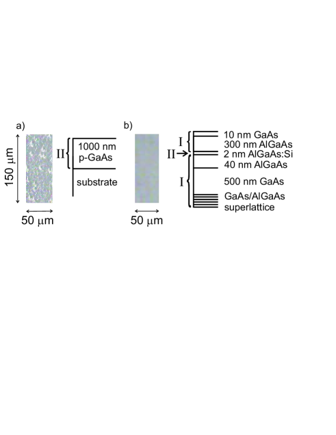
Growing a thick p-doped layer under such conditions, resulted in a surface covered with large, triangular-shaped defects (Fig. 2a) as observed
previously
Tok et al. (1998).
We define the acceptor efficiency as the ratio of Si-acceptors to the total number of incorporated silicon atoms and the compensation ratio as the ratio of Si-acceptors to Si donors . We calibrate assuming a
Si-acceptor doping efficiency of
for n-type GaAs on a oriented substrate.
Samples with an acceptor density increased to exhibit a metallic behavior down to 4.2 K.
The hole density is with for .
The low density sample has at . With at room temperature one deduces
at a Si density of at .
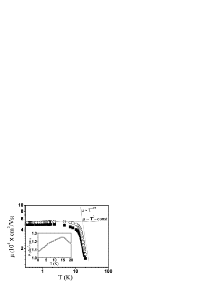
Transport in the heavily auto-compensated insulating sample is well-described by hopping conduction in a parallel impurity band. The temperature dependence of the Hall coefficient of this sample (Fig. 1)
is expected to show the following functional form (following the notation of Shklovskii and Efros (1984)):
with the longitudinal resistance (inset Fig. 1)
for and for .
This is typical for lightly bulk-doped semiconductors with conduction in the valence band and in an impurity band, with the activated behavior characterizing the nearest neighbor hopping gap Shklovskii and Efros (1984).
The deduced acceptor activation energy
is about a factor of smaller than the activation energy of isolated Si-acceptors in GaAs obtained by Hall-effect measurements Sze (1981). Taking into account that the activation energy in doped semiconductors decreases according to Schubert (1993), the measured is lower than the expected one
and may be due to an impurity band strongly broadened towards the valence band.
From the value of in the saturation regime for low temperatures where the valance band holes are frozen out, one can deduce the number of hopping conductors involved in transport,
leading to
A discrepancy between and has been also observed
previously Arushanov et al. (1994)
with the former being relevant for low-temperature applications.

Now we can compare the experimental results with the theoretical expectations for the MIT.
The metal-insulator transition is defined by the Mott criterion , with the effective Bohr radius and the critical transition density Schubert (1993) which can be estimated to for acceptors in p-type GaAs. The deduced acceptor concentration
showing insulating behavior is well below the critical density of the MIT. In
agreement with the theory the density
showing metallic behavior is above the critical density of the MIT.
The rest of the article discusses the two-dimensional hole gas, which was fabricated by using a thin layer of the metallic p-type material as a modulation doping.
To overcome the problem of the poor surface morphology and the consequent bad mobility, we grew the modulation doped heterostructure by using two different growth conditions.
We used type I growth conditions up to the doping layer. Then we changed to type II for the doping and switched back to type I conditions (Fig. 2b).
This resulted in a very good surface morphology for the 2DHG growth (Fig. 2b), comparable to 2DEG heterostructures grown on GaAs Fischer et al. (2004).
We studied the sample quality with measurements of the longitudinal and
transverse resistance with a special focus on the low B-field Shubnikov-de Haas oscillations (SdH).
The highest observed hole mobility is at a density of indicating the excellent quality of the samples despite the doping layer with the poor morphology. An ungated sample shows very well developed quantum Hall plateaus and minima of the longitudinal resistance at (Fig. 3). In the low B-Field regime one can observe a beating of the SdH (Fig. 3) which is known from literature for 2DHGs Stormer et al. (1983)
to arise from zero-field spin splitting because of inversion asymmetry Winkler (2003). By plotting against and Fourier transforming it Habib et al. (2004) in the low B-Field region (inset Fig. 3) one can directly deduce the density of of the lower spin subband and the density of the upper subband which add up to the total density evident at high B-fields .

We studied persistent photoconductivity (PPC) which is a common technique to increase the carrier density in two-dimensional electron systems (2DES)
though it is uncommon in 2DHGs Störmer et al. (1983).
We find a pronounced PPC effect in our samples.
The unilluminated, dark density of the 2DHG at is with a mobility of
. By illuminating a Hall-bar sample with a LED we were able to tune the density up to the maximum density of with a mobility
at .
By using an L-shaped Hall-bar we investigate the mobility anisotropy of the two principal in-plane directions
and .
A considerable mobility anisotropy has been reported in literature for
2DHGs in GaAs Henini et al. (1995a). Up to a factor of 4 anisotropy has been observed in Si-doped systems and different Be-doped facets and is partially due to anisotropic interface roughness scattering Heremans et al. (1994) and the anisotropic effective mass.
Henini, et al. Henini et al. (1995b) found that in Be-doped 2DHGs the mobility along is about a factor of 3 larger than the mobility along at a density of . In contrast, in our samples we observed only a very weak anisotropy
mostly pronounced at low temperatures where it is within
a factor of to .
Fig. 4 shows that the mobility is nearly constant for in both directions and that for , .
From anisotropies in the bulk mass alone, one would expect a mobility anisotropy of a factor of 0.5, leaving open the possibility that anisotropic roughness may be counteracting the mass anisotropy.
In summary we
characterized heavily autocompensated Si-doped bulk (110) GaAs, and observed an insulating impurity band for a non-degenerate bulk p-type sample below the MIT, and metallic conduction for a degeneratly doped sample. We were able to grow the first high mobility 2DHG on oriented GaAs using Si as a dopant. We observed an unusual PPC and a weak anisotropy.
High mobility MBE systems, equipped with Si as the only dopant source can take advantage of this new technique to grow 2DHGs on oriented GaAs. Since the orientation is the natural cleavage plane of GaAs, it should also be possible to grow 2DHGs by cleaved edge overgrowth (CEO) Pfeiffer et al. (1997) without introducing additional dopant sources. This enables new devices like atomically precise hole wires and orthogonal 2D-2D tunnel-junctions, for probing the quantum Hall edges of a 2DHG analogous to previous studies in electron systems Huber et al. (2004). It also permits bipolar n-p heterostructures to be prepared in standard III-V growth chambers.
Acknowledgements.
This work was supported financially by Deutsche Forschungsgemeinschaft via Schwerpunktprogramm Quantum-Hall-Systeme and in the framework of the COLLECT EC-Research Training Network HPRN-CT-2002-00291.References
- Winkler (2003) R. Winkler, Spin-orbit Coupling Effects in Two-Dimensional Electron and Hole Systems (Springer Verlag, 2003).
- Papadakis et al. (2000) S. J. Papadakis, E. P. D. Poortere, M. Shayegan, and R. Winkler, Phys. Rev. Lett. 84, 5592 (2000).
- Stormer and Tsang (1980) H. L. Stormer and W.-T. Tsang, Appl. Phys. Lett. 36, 685 (1980).
- Wieck and Reuter (2000) A. Wieck and D. Reuter, Inst. Phys. Conf. Ser. 166, 51 (2000).
- Tok et al. (1998) E. S. Tok, J. H. Neave, M. J. Ashwin, B. A. Joyce, and T. S. Jones, J. of Appl. Phys. 83, 4160 (1998).
- Shklovskii and Efros (1984) B. Shklovskii and A. Efros, Electronic Properties of Doped Semiconductors (Springer Verlag, 1984).
- Sze (1981) S. Sze, Physics of Semiconductor Devices (Wiley, 1981).
- Schubert (1993) E. Schubert, Doping in III-V semiconductors (Cambridge University Press, 1993).
- Arushanov et al. (1994) E. Arushanov, C. Kloc, and E. Bucher, Phys. Rev. B 50, 2653 (1994).
- Fischer et al. (2004) F. Fischer, M. Grayson, E. Schuberth, D. Schuh, M. Bichler, and G. Abstreiter, Physica E 22, 108 (2004).
- Stormer et al. (1983) H. L. Stormer, Z. Schlesinger, A. Chang, D. C. Tsui, A. C. Gossard, and W. Wiegmann, Phys. Rev. Lett. 51, 126 (1983).
- Habib et al. (2004) B. Habib, E. Tutuc, S. Melinte, M. Shayegan, D. Wasserman, S. A. Lyon, and R. Winkler, Phys. Rev. B 69, 113311 (pages 4) (2004).
- Störmer et al. (1983) H. Störmer, A. Gossard, W. Wiegmann, R. Blondel, and K. Baldwin, Appl. Phys. Lett. 44, 139 (1983).
- Henini et al. (1995a) M. Henini, P. Rodgers, P. Crump, B. Gallagher, and G. Hill, J. Cryst. Growth 150, 451 (1995a).
- Heremans et al. (1994) J. J. Heremans, M. B. Santos, K. Hirakawa, and M. Shayegan, J. of Appl. Phys. 76, 1980 (1994).
- Henini et al. (1995b) M. Henini, P. Crump, P. Rodgers, B. Gallagher, A. Vickers, and G. Hill, J. Cryst. Growth 150, 446 (1995b).
- Pfeiffer et al. (1997) L. Pfeiffer, K. West, H. Stormer, J. Eisenstein, K. Baldwin, and D. Gershoni, Appl. Phys. Lett. 56, 1697 (1997).
- Huber et al. (2004) M. Huber, M. Grayson, D. Schuh, M. Bichler, W. Biberacher, W. Wegscheider, and G. Abstreiter, Physica E 22, 164 (2004).