Defective transport properties of three-terminal carbon nanotube junctions
Abstract
We investigate the transport properties of three terminal carbon based nanojunctions within the scattering matrix approach. The stability of such junctions is subordinated to the presence of nonhexagonal arrangements in the molecular network. Such “defective” arrangements do influence the resulting quantum transport observables, as a consequence of the possibility of acting as pinning centers of the correspondent wavefunction. By investigating a fairly wide class of junctions we have found regular mutual dependencies between such localized states at the carbon network and a strikingly behavior of the conductance. In particular, we have shown that Fano resonances emerge as a natural result of the interference between defective states and the extended continuum background. As a consequence, the currents through the junctions hitting these resonant states might experience variations on a relevant scale with current modulations of up to 75%.
pacs:
73.22.-f, 73.40.Sx, 73.63.-Fg, 81.07.De, 85.35.KtI Introduction
Molecular electronics is a promising candidate in our way towards smaller electronic devices and a lot of effort has been put, in the last decades since the first proposal in this direction,Aviram and Ratner (1974) into making it a feasible goal for the near future. Nevertheless, there is still a lot of work to be done in order to understand the behavior of nanodevices and fully exploit their nontrivial quantum effects dominating the physical and chemical properties at the nanometer level.Cuniberti et al. (2005)
Our interest will focus on carbon nanotubes (CNTs), which are
basically rolled up graphitic sheets.
CNTs have been
proposed as leads and bridge molecules, since they possess a great versatility,
allowing for metallic as well as semiconducting behavior,Saito et al. (1998); Yi et al. (2004)
depending on their diameter and chirality, that
is, their degree of helicity. Nanotubes can be easily modified by
introducing pentagons, heptagons or octagons into their hexagonal network, as
was already shownIijima et al. (1992); Ihara et al. (1993) soon after their
discovery.Iijima (1991)
By joining a metallic nanotube with a semiconducting one, a
heterojunction is formed showing a transport behavior corresponding to
that of a rectifying diode, as already seen experimentally;Yao et al. (1999)
actually several applications of CNTs in
nanoscale devices have been already
described.Postma et al. (2001); Javey et al. (2003); Misewich et al. (2003); Rueckes et al. (2000); Heinze et al.
Yet, for making efficient molecular electronic circuits
multi-probe junctions are also needed and their transport
characteristics must be understood.Yi and Cuniberti (2003) Three-terminal
junctions are especially appropriate for these studies, as they
can be taken as building blocks of multi-terminal junctions. The
understanding of the transport properties of these three-terminal
systems is the goal of this work.
The first experimental observation of three-terminal CNTs were as
branches in L-, T-, and Y-patterns occurring during the growth of
carbon nanotubes produced in an arc-discharge
method,Zhou and Seraphin (1995) but the formation of these junctions was
totally random. Since then, new growth methods have been developed
to obtain these multi-terminal junctions in a more controlled and
high-yield production way: a template-based pyrolytic technique
which yields large numbers of well-aligned Y-junctions of
multi-walled CNTs (MWCNTs, a coaxial arrangement of
CNTs),Li et al. (1999); Sui et al. (2001) a hot filament chemical vapor
deposition (CVD) system where uniformly Y-shaped junctions are
obtained as by-product, with structures that match those of
topological models where only heptagons are included as defects in
the hexagonal network,Gan et al. (2000a) or pyrolysis of
nickelocene in the presence of thiophene,Satishkumar et al. (2000)
or of ferrocene and cobaltocene.Deepak et al. (2001) Also a simple
thermal catalyst CVD method without templates yields a production
of H- and Y-junctions as well as
3D-CNT-webs.Ting and Chang (2002); Zhu et al. (2002) All these last methods are
characterized by growth temperatures just moderately high
(-) or even quite low (room temperature).
But also the high-temperature arc-discharge technique has been improved
to produce Y-junctions in a reasonable
proportion.Klusek et al. (2002); Osváth et al. (2002)
Nearly at the same time, the first observations of three-terminal
single-walled CNTs (SWCNTs) were made where the junctions were
produced by thermal decomposition of fullerenesNagy et al. (2000) or
by more sophisticated methods including electron irradiation on
welded nanotubes to finally tailor the transformation of the
junction geometry with the formation of heptagonal and octagonal
defects.Terrones et al. (2002)
By now, it has been made clear that Y-junctions are not any more a rare phenomenon. Actually taking into account all the different methods which yield similar CNT Y-junctions, these have to be accepted as regular members of the carbon nanostructure family. Although less experimental data is available, transport measurements have been carried out on nanotube junctions, by overlaying one individual SWCNT over another with four electrical contacts where a good tunnel contact at the junction is observed,Fuhrer et al. (2000) or measuring the - characteristics of truly Y-junction MWCNTs which behave as intrinsic nonlinear and asymmetric devices, displaying a clear rectifying behavior.Satishkumar et al. (2000); Papadopoulos et al. (2000) Moreover the transport properties of three-terminal junctions obtained by merging together SWNTs via molecular linkers have also been studied.Chiu et al. (2004)
From the theoretical point of view, much work has been done to clarify the structure of these junctions as well as their intrinsic transport properties. To provide an accurate description of quantum transport in CNT-junctions one cannot neglect their electronic structure via an atomistic model. Theoretical predictions are then based on hypothesized atomic configurations, which try to match the experimental observations on branching angles and tube diameters. But especially the latter have always a wide uncertainty. Most of the experiments on Y-junctions are nevertheless dealing with MWCNTs and even with a fish-bone like structure as some growth methods do not achieve a complete graphitization of the tubes. There is therefore still a need for a better experimental characterization of the junctions. Different approaches have been followed to come up with different proposed structures, like considering the junction as evolved from two bend tubesGan et al. (2000b) or by considering that three carbon nanotubes join via two triangular central spacers.Treboux et al. (1999) But no matter how this structure is reached, non-hexagonal elements must be included in the honeycomb-like lattice, following the generalized Euler rule,Crespi (1998) which predicts a bond surplus of six for three-terminal junctions. These pentagons, heptagons or octagons are playing an important role in the transport properties characterizing these junctions, with an electronic structure which differs considerably from that of the nanotube “bulk” region. Thus several groupsScuseria (1992); Chernozatonskii (1992); Menon and Srivastava (1997); Treboux et al. (1999); Pérez-Garrido and Urbina (2002) have analyzed the geometry of multi-terminal junctions and its stability using topological arguments, molecular dynamics techniques or first-principle methods. The role of the symmetry of the junctions and of the chirality of the arms is also addressed by many authorsAndriotis et al. (2001, 2002); Meunier et al. (2002); Menon et al. (2003) as well as the electronic interaction.Chen et al. (2002) However, the controversy remains over the origin of the rectifying behavior, with some studies claiming it to be a characteristic intrinsic to the symmetry of the junction,Andriotis et al. (2002) and other works tracing it back to the interfaces with contacts.Meunier et al. (2002)
Until now Fano resonances have not been exploited as an interesting feature in the transport through this kind of CNT junctions. This phenomenon emerges from the coherent interaction of a discrete state and a continuum and was first discovered by studying the asymmetric peaks of the helium spectrum.Fano (1961) Recently the occurrence of this effect and its applications have been studied in numerous mesoscopic devices, including MWCNTsKim et al. (2003); Zhang et al. (2003) and MWCNT bundlesYi et al. (2003) or SWNT bundles,Babic and Schönenberger (2004) and most recently in multiply-connected CNTs.Kim et al. (2004) As we will see the conductance through multi-terminal CNT junctions exhibits Fano resonances and these may be used in transport allowing for major changes of the current intensity in short intervals.
The aim of this work is the calculation of transmissions and conductances for different types of three-terminal CNTs, keeping in mind the properties of semi-infinite CNTs considered as partial components of our system analyzed before.Del Valle et al.
The paper is organized as follows: we will firstly explain the method used in our calculations and introduce the different junctions which will focus our attention in this paper. The presentation and a brief discussion of the results for the different transport properties will follow in Sec. III and will be concluded in Sec. IV.
II System and Method
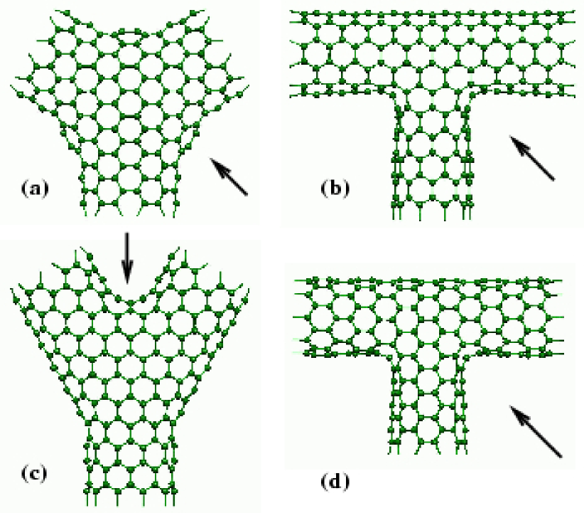
Fig. 1 shows four archetypical three-terminal CNT devices. These devices have a much greater versatility than two-terminal junctions as the third terminal can be used to apply a gate voltage and thus control the current flow in the channel built by the two other arms, using the gate as a current probe or as a voltage probe. Out of the many possibilities of building three-terminal junctions, we have chosen these four as to have within a few junctions different elements of comparison: different symmetries, different geometries, different chiralities. These junctions have nevertheless common properties, from which in conjunction with their disparities we may draw some general conclusions. As a model for nanoelectrodes, we will use semi-infinite carbon nanotubes and try to gain insight in the quantum transport through these junctions. We calculate the quantum conductance within the well-known Landauer-Büttiker formalismLandauer (1987); Büttiker (1988) by making use of equilibrium Green functions for tight-binding Hamiltonians.Cuniberti et al. (2002) Our structures have been optimized by a relaxation algorithm following a density-functional based nonorthogonal tight-binding scheme (DFTB)Elstner et al. (1998) in order to deal with stable structures. This method is an extension of the tight-binding formalism, based on a second-order expansion of the Kohn-Sham total energy in density-functional theory with respect to charge density fluctuations. Besides the usual short-range repulsive terms the final approximate Kohn-Sham energy additionally includes a Coulomb interaction between charge fluctuations. The basis set used is minimal but conveniently optimized for carbon atoms.
The semi-infinite leads are treated with a decimation technique, an application of the renormalization-group method which allows us to calculate the electronic properties of extended systems with a low computational cost. We follow the iterative procedure to decimate the individual layersdec and operate in the space of localized orbitals. As principal layers for our system, we take slices of the CNT and for convenience we choose the CNT unit cell as unit slice. In this way, we renormalized out slices after iteration steps, and this exponential behavior allows us to quickly achieve convergence.
The systems considered are all-carbon devices for which a orbital description level has been proved to yield very satisfactory quantitative results,Saito et al. (1998) since the properties of carbon nanotubes are basically determined by orbitals.
The Hamiltonian describing our system can be written in a very compact form:
| (1) |
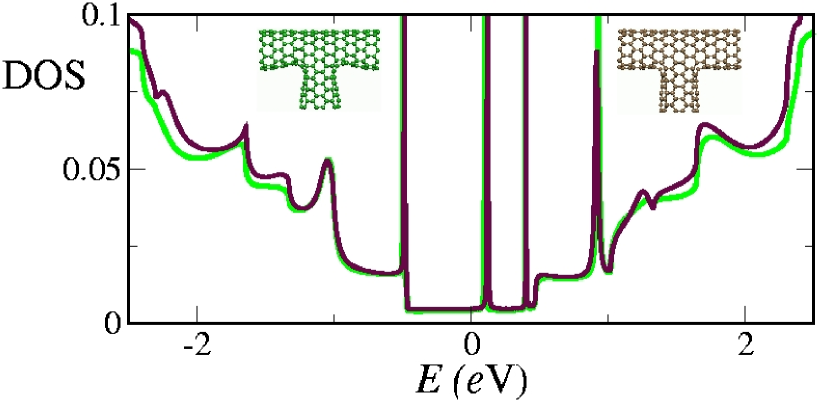
where is the coupling or hopping parameter. This transfer integral is only non-zero between nearest-neighbors and takes the value of V. We have also made this parameter distance-dependent, but no significant changes are observed. This can be seen in Fig. 2, where the DOS is plotted for one of the T-junctions for which another relaxation was available, making a comparison possible. The DOS calculated with distance-dependent hopping parameters for two differently relaxed structures show an almost identical behavior at low energies.
For calculating the conductance, we divide the system into a central region or scatterer (S) and the three leads (, , ). The Green function for our system, , can be written in terms of block matrices
| (6) | |||
| (11) |
where the different leads are independent as we restrict our calculations to nearest-neighbor interaction throughout the whole system. Note that and are infinite-dimensional matrices. It is straightforward now to obtain via a Dyson equation an explicit expression for , which has now only finite matrices:
| (12) |
where we define as the self-energy terms containing the contribution of the semi-infinite leads
| (13) |
being , or and the lead Green functions. And these functions are calculated using the decimation technique mentioned above:
| (14) |
where is the number of steps necessary to achieve convergence in the iteration process given by
| (15) | |||||
| (16) | |||||
| (17) | |||||
| (18) |
for which we have defined
| (19) | |||||
| (20) | |||||
| (21) |
where is the Hamiltonian describing any of the principal layers or slices in which we have divided up the lead, i.e. the projection of onto the space of this slice. These slices are coupled to their nearest-neighbor layers in the lead through the interactions described by .
With the lead Green functions we can easily calculate the strength of the coupling of the scatterer to the leads
| (22) |
Using all these definitions, we can write the conductance function in a very compact form:
| (23) |
where the factor two accounts for the spin degeneracy. The Landauer-Büttiker formula relates the conductance in a multi-terminal conductor to its scattering properties. For the three terminal case, if we take one of the leads to be a voltage probe (say for instance lead ), we constrain the chemical potential in this arm to beBüttiker (1988)
| (24) |
Although this constriction assures a zero current at terminal , this probe is dissipative as the carriers in it loose their phase memory, accounting for a phase-incoherent contribution to the coherent current of carriers reaching directly probe from . The total conductance can then be written as , where
| (25) |
For our systems the inelastic contribution to the conductance is very small at energies around the Fermi level.
The current measured in this way is then
| (26) |
where is the Fermi function in the lead , , , and is the total transmission between lead and such that . The voltage drop is small enough to validate the linear-response regime, and we restrict our calculations to the zero temperature limit.
III Transport properties
We have studied different types of SWCNT junctions, from which four are now presented in Fig. 1, chosen in such a way that a variety of heterojunction combinations and a variety of shapes are covered. In these junctions the following groups of three semiinfinite CNTs welded together: in a Y-shape, , both Y- and T-shaped, and with a T shape. Two types of CNT leads have been adopted: armchair tubes and zigzag tubes. As known CNTs, where are the indexes unambiguously determining the characteristics of the CNT, are metallic if is a multiple of three, neglecting the hybridization. We thus have a metallic tube, the CNT and a semiconducting one, the exhibiting a gap of V. Then by using just these two different CNTs we are able to make M-M and M-S heterojunctions (where M stands for metallic and S for semiconducting).

In the chosen configurations, one of the terminals is taken to be either a voltage probe or a current probe. This gate voltage is controlled in our model by changing the onsite energies of this arm, which are fixed at a far end of the terminal and gradually change in the central region to meet the value set for the other two arms and the junction.
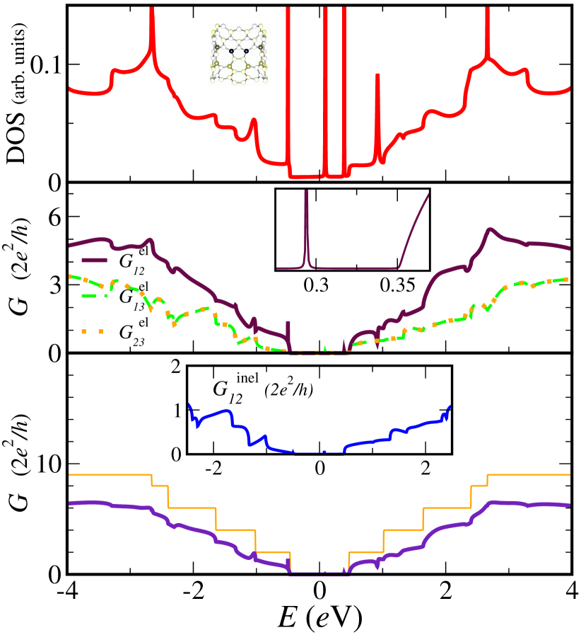
We will now proceed to describe the obtained results for the DOS and conductance of these junctions, which are given in Figs. 3, 4, 5 and 6.
Let us consider the electronic structure of the first Y-junction (Fig. 1.a), a highly symmetric junction where three metallic armchair nanotubes intersect at . This structure has mirror symmetry with respect to four planes, being thus the most symmetrical of all four studied junctions, as the other three are characterized by two mirror planes. The necessary negative curvature is provided by the introduction of heptagonal defects, in a number of six to meet the topological constraints imposed by Euler theorem, and distributed symmetrically, two at each saddle region.
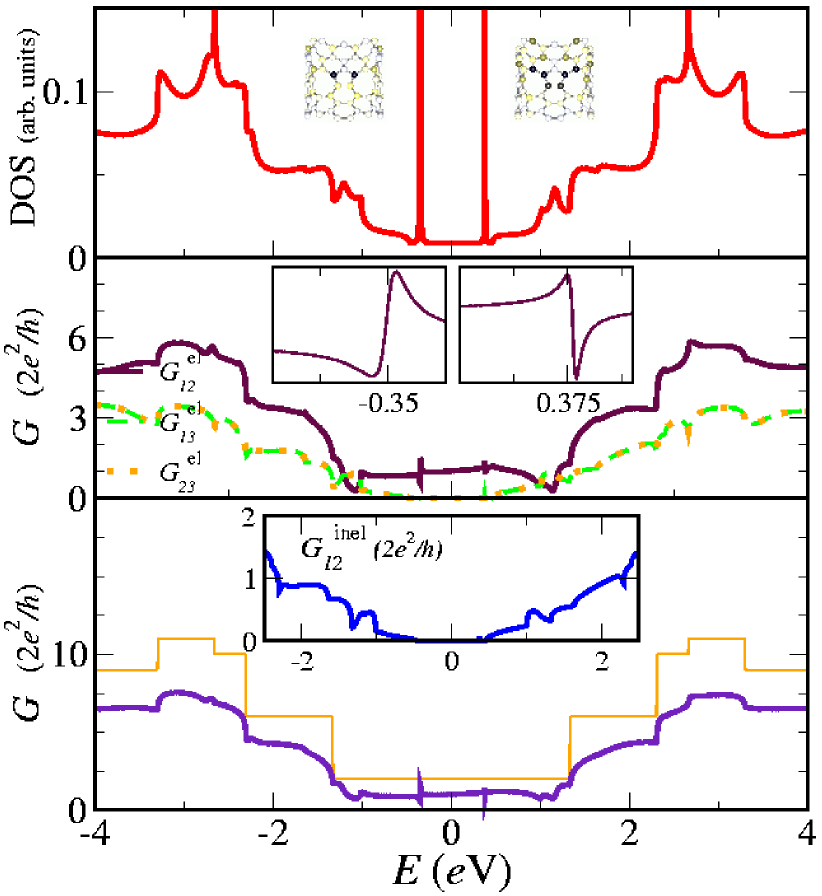
This junction shows a metallic behavior, but the transmission probability around the Fermi level is small as seen in the lower panel of Fig. 3. The localization of the states at the Fermi energy is schematically seen in the inset of this figure, showing that this is an extended state but also pinned by the defects. This is an effect we see along all the different junctions. It is known that heptagons and pentagons can induce additional electronic states close to the Fermi energy,Menon and Srivastava (1997); Klusek et al. (2002) which are seen here (upper panel of Fig. 3) between the subbands.
The first T-junction (Fig. 1.b) is made up of two metallic armchair nanotubes and a semiconducting zigzag nanotube. This is achieved by introducing two octagons and one pentagon at each bending point. This junction also shows a metallic behavior (upper panel of Fig. 4) although one of its branches has a semiconducting character. Remarkable are the two sharp peaks located symmetrically around the Fermi level (approximately at V below and above it). The distribution of these states in the area of the non-hexagonal defects is seen in the upper insets of Fig. 4. These are states which do not extend at all to the upper part of the junction and are mainly localized at the defects. To corroborate this thesis, we have checked the behavior of the local density of states (LDOS) at the resonant energies. The presence of both extended states and localized defective states in the junction creates the conditions for the Fano resonance to be observed.Fano (1961)
The resonance-like structure in the transmission exhibits indeed asymmetric line shapes resembling those of Fano resonances. These line shapes result from the interaction of a discrete state with a continuum of metallic states. The degree of asymmetry of these curves is determined by the so-called Fano parameter, which changes here its sign. Therefore at the resonances we have that where is the Fano parameter and is the undressed Green function for the continuum. Due to the analyticity properties of the Green functions (causality), the real and imaginary parts of are related by a Kramers-Kronig (Hilbert) transformation:
| (27) |
where means principal value. From these equations, we see that for an asymmetric DOS with most of its weight situated at frequencies below the energy in a small window around this energy, it is likely to obtain , whereas for asymmetric DOS with more weight at , is likely negative. The shape of the DOS of the continuum of states of this metallic junction decreases rapidly before the left peak, and increases just after the one to the right. This accounts for the different signs of as observed in the plot. Though the states around are the most significant for determining the sign of , it is necessary to take into account the whole range of energy of the band.

These characteristics are then observed in the - curves (Fig. 7.b), though its effect is not that of a switch-off of the current, as the transmission background of the continuum is too strong. Nevertheless differences in the current amplitude up to 30% are observed.
The second Y-junction, shown in Fig. 1.c, is made up with the same combination of leads as the previous T-junction, but forcing now the armchair tubes to bend, forming a Y-shape. In this case, we have a very different rearrangement of the defects. Four of the heptagons are situated on the upper saddle while the other two are shared by the obtuse angles. The junction is indeed metallic, as shown in Fig. 5, but as in the previous case quickly assumes the electronic character of the corresponding arms. Above the Fermi energy, the necessary conditions for a Fano resonance appear again. The sharp peak of a localized state is seen in the DOS and its corresponding Fano resonance in the conductance. Its behavior all in all resembles that of the junction in Fig. 1.b but anyhow presents remarkable differences, as a greater asymmetry, which are exclusively due to the junction shape and the situation of the defects.
The - characteristics of this junction shown in Fig. 7.c present an interesting profile, as the big change in current makes it interesting for its use as a circuit component.
The last of the presented junctions shown in Fig. 1.d is again a T-shaped one but built up of one metallic and two semiconducting tubes. Like in the other T junction the defects are octagons and pentagons, distributed symmetrically in both bending regions. The transport properties of this junction, given in Fig. 6, are dominated by the semiconducting behavior of the upper branches, whose gap is reflected in the conductance of this junction. A non-equilibrium study of its properties would be necessary to fully explore its possible applications in electronics.
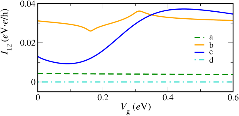
The influence of the gate voltage on the current is shown in Fig. 7. Here the current flowing between the upper branches is calculated under a small bias voltage of the order of a few tens of mV, while we smoothly change a gate voltage which shifts the levels of the orbitals at the third arm of the junction. We should stress at this point that the bias voltages used in this calculation allows us to remain within the linear response regime. As can be seen the current suffers a great modulation in some of the junctions, increasing its amplitude in up to 75%.
Despite the fact that our model is adequate for getting linear response, we apply it to a nonlinear situation for sheer comparison of our results to previous calculations.Andriotis et al. (2002) We calculate the - characteristics of these junctions considering different possible experimental setups. In Fig. 8 we report the current through the third lead in two different situations: first the upper branches are grounded and the third lead is biased with a voltage . That is,
| (28) |
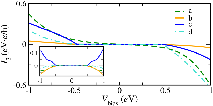
Under these conditions a certain degree of rectification power is present in the setup, but the rectification is not an inherent property of the junctions. This can be seen in a second case where the third lead is grounded while a bias is applied between the first and second lead, i.e. when plotting the current versus the bias voltage for the setup
| (29) |
as shown in the inset of the same figure. The degree of asymmetry in view at the - curves when using the first of the experimental setups disappears for the second setup. In this case the current curves are symmetrical with respect to the bias voltage, both for , plotted in the inset, as for the current flow through the upper arms.
IV Discussion and conclusions
By making use of the Landauer formalism and equilibrium Green functions techniques, we have studied the transport properties of different carbon nanotube junctions, at an atomistic description level, and paid especial attention to bound states. Our analysis of the conductance behavior of several three terminal carbon nanotube junctions allows us to identify common patterns and draw general conclusions. This can be done by sorting out different factors in the qualitative features of the conductance, namely (i) the role of structural defects in the molecular network, (ii) the resulting geometrical symmetry properties, and (iii) the electronic nature of the contacted leads (whether metallic or semiconducting tubes). By opening the energy of the electron incoming in the injecting lead one encounters typical resonant behaviors of the LDOS.mov For such energies most spectral power is associated to the defective atoms at the saddle regions. The presence of background states, mostly contributed by the attached leads, creates the conditions for an interference between localized and extended states, with the appearance of the so-called Fano resonance. Indeed resonant defective states in the DOS are paired by the typical Fano line shape of the form
| (30) |
This feature could be eventually detectable in experiments, as differences in current amplitude up to 75% are observed when using one arm of the three-terminal as a gate electrode. We have thus shown how through the localized states, we can control the current flow through the upper branches which is driven by a bias voltage applied across the first two terminals.
Acknowledgements.
We are indebted to Marieta Gheorghe and Pasquale Pavone for helpful support at different stages of this work, and to Antonio Pérez Garrido for providing us with the coordinates of one of the junctions. MD acknowledges the support from the FPI Program of the Comunidad Autónoma de Madrid. This work was funded by the Volkswagen Foundation (Germany), by the MCYT (Spain) under the contract MAT2002-00139, by the EU within the RTN COLLECT and by the EU-FET program under contract IST-2001-38951.References
- Aviram and Ratner (1974) A. Aviram and M. A. Ratner, Chem. Phy. Lett. 29, 277 (1974).
- Cuniberti et al. (2005) G. Cuniberti, G. Fagas, and K. Richter, eds., Introducing Molecular Electronics (Springer, Berlin, 2005).
- Saito et al. (1998) R. Saito, G. Dresselhaus, and M. S. Dresselhaus, Physical Properties of Carbon Nanotubes (Imperial College Press, London, 1998), ISBN 1-86094-093-5.
- Yi et al. (2004) J. Yi, M. Porto, and G. Cuniberti, Encyclopedia of Nanoscience and Nanotechnology, vol. 5 (American Scientific Publishers, California, 2004), ISBN 1-58883-001-2.
- Iijima et al. (1992) S. Iijima, T. Ichihashi, and Y. Ando, Nature 356, 776 (1992).
- Ihara et al. (1993) S. Ihara, S. Itoh, and J. Kitakami, Phys. Rev. B 48, 5643 (1993).
- Iijima (1991) S. Iijima, Nature 354, 56 (1991).
- Yao et al. (1999) Z. Yao, H. W. C. Postma, L. Balents, and C. Dekker, Nature 402, 273 (1999).
- Postma et al. (2001) H. W. C. Postma, T. Teepen, Z. Yao, M. Grifoni, and C. Dekker, Science 293, 76 (2001).
- Javey et al. (2003) A. Javey, J. Guo, Q. Wang, M. Lundstrom, and H. Dai, Nature 424, 654 (2003).
- Misewich et al. (2003) J. A. Misewich, R. Martel, P. Avouris, J. C. Tsang, S. Heinze, and J. Tersoff, Science 300, 783 (2003).
- Rueckes et al. (2000) T. Rueckes, K. Kim, E. Joselevich, G. Y. Tseng, C.-L. Cheung, and C. M. Lieber, Science 289, 94 (2000).
- (13) S. Heinze, J. Tersoff, and P. Avouris, in Ref. Cuniberti et al., 2005.
- Yi and Cuniberti (2003) J. Yi and G. Cuniberti, Annals of the New York Academy of Sciences 1006, 306 (2003).
- Zhou and Seraphin (1995) D. Zhou and S. Seraphin, Chem. Phy. Lett. 238, 286 (1995).
- Li et al. (1999) J. Li, C. Papadopoulos, and J. Xu, Nature 402, 253 (1999).
- Sui et al. (2001) Y. C. Sui, J. A. González-León, A. Bermúdez, and J. M. Saniger, Carbon 39, 1709 (2001).
- Gan et al. (2000a) B. Gan, J. Ahn, Q. Zhang, S. F. Yoon, Rusli, Q. F. Huang, H. Yang, M. B. Yu, and W. Z. Li, Diamond and Related Materials 9, 897 (2000a).
- Satishkumar et al. (2000) B. C. Satishkumar, P. J. Thomas, A. Govindaraj, and C. N. R. Rao, Appl. Phys. Lett. 77, 2530 (2000).
- Deepak et al. (2001) F. L. Deepak, A. Govindaraj, and C. N. R. Rao, Chem. Phy. Lett. 345, 5 (2001).
- Ting and Chang (2002) J.-M. Ting and C.-C. Chang, Appl. Phys. Lett. 80, 324 (2002).
- Zhu et al. (2002) H. Zhu, L. Ci, C. Xu, J. Liang, and D. Wu, Diamond and Related Materials 11, 1349 (2002).
- Klusek et al. (2002) Z. Klusek, S. Datta, P. Byszewski, P. Kowalczyk, and W. Kozlowski, Surface Science 507-510, 577 (2002).
- Osváth et al. (2002) Z. Osváth, A. A. Koós, Z. E. Horváth, J. Gyulai, A. M. Benito, M. T. Martínez, W. K. Maser, and L. P. Biró, Chem. Phy. Lett. 365, 338 (2002).
- Nagy et al. (2000) P. Nagy, R. Ehlich, L. P. Biró, and J. Gyulai, Appl. Phys. A 70, 481 (2000).
- Terrones et al. (2002) M. Terrones, F. Banhart, N. Grobert, J.-C. Charlier, H. Terrones, and P. M. Ajayan, Phys. Rev. Lett. 89, 075505 (2002).
- Fuhrer et al. (2000) M. S. Fuhrer, J. Nygård, L. Shih, M. Forero, Y.-G. Yoon, M. S. C. Mazzoni, H. J. Choi, J. Ihm, S. G. Louie, A. Zettl, et al., Science 288, 494 (2000).
- Papadopoulos et al. (2000) C. Papadopoulos, A. Rakitin, J. Li, A. S. Vedeneev, and J. M. Xu, Phys. Rev. Lett. 85, 3476 (2000).
- Chiu et al. (2004) P. W. Chiu, M. Kaempgen, and S. Roth, Phys. Rev. Lett. 92, 246802 (2004).
- Gan et al. (2000b) B. Gan, J. Ahn, Q. Zhang, Q. F. Huang, C. Kerlit, S. F. Yoon, Rusli, V. A. Ligachev, X.-B. Zhang, and W.-Z. Li, Materials Letters 45, 315 (2000b).
- Treboux et al. (1999) G. Treboux, P. Lapstun, and K. Silverbrook, Chem. Phy. Lett. 306, 402 (1999).
- Crespi (1998) V. H. Crespi, Phys. Rev. B 58, 12671 (1998).
- Scuseria (1992) G. E. Scuseria, Chem. Phy. Lett. 195, 534 (1992).
- Chernozatonskii (1992) L. A. Chernozatonskii, Phys. Lett. A 172, 173 (1992).
- Menon and Srivastava (1997) M. Menon and D. Srivastava, Phys. Rev. Lett. 79, 4453 (1997).
- Pérez-Garrido and Urbina (2002) A. Pérez-Garrido and A. Urbina, Carbon 40, 1227 (2002).
- Andriotis et al. (2001) A. N. Andriotis, M. Menon, D. Srivastava, and L. Chernozatonskii, Appl. Phys. Lett. 79, 266 (2001).
- Andriotis et al. (2002) A. N. Andriotis, M. Menon, D. Srivastava, and L. Chernozatonskii, Phys. Rev. B 65, 165416 (2002).
- Meunier et al. (2002) V. Meunier, M. B. Nardelli, J. Bernholc, T. Zacharia, and J.-C. Charlier, Appl. Phys. Lett. 81, 5234 (2002).
- Menon et al. (2003) M. Menon, A. N. Andriotis, D. Srivastava, I. Ponomareva, and L. Chernozatonskii, Phys. Rev. Lett. 91, 145501 (2003).
- Chen et al. (2002) S. Chen, B. Trauzettel, and R. Egger, Phys. Rev. Lett. 89, 226404 (2002).
- Fano (1961) U. Fano, Phys. Rev. 124, 1866 (1961).
- Kim et al. (2003) J. Kim, J.-R. Kim, J.-O. Lee, J. W. Park, H. M. So, N. Kim, K. Kang, K.-H. Yoo, and J.-J. Kim, Phys. Rev. Lett. 90, 166403 (2003).
- Zhang et al. (2003) Z. Zhang, V. Chandrasekhar, D. A. Dikin, and R. S. Ruoff, cond-mat/0311360 (2003).
- Yi et al. (2003) W. Yi, L. Lu, H. Hu, Z. W. Pan, and S. S. Xie, Phys. Rev. Lett. 91, 076801 (2003).
- Babic and Schönenberger (2004) B. Babic and C. Schönenberger, Phys. Rev. B (2004).
- Kim et al. (2004) G. Kim, S. B. Lee, T.-S. Kim, and J. Ihm (2004).
- (48) M. Del Valle, C. Tejedor, and G. Cuniberti, in preparation.
- Landauer (1987) R. Landauer, Zeitschrift für Physik B 68, 217 (1987).
- Büttiker (1988) M. Büttiker, IBM J. Res. Develop. 32, 317 (1988).
- Cuniberti et al. (2002) G. Cuniberti, F. Großmann, and R. Gutiérrez, Adv. in Sol. Stat. Phys. 42, 133 (2002).
- Elstner et al. (1998) M. Elstner, D. Porezag, G. Jungnickel, J. Elsner, M. Haugk, T. Frauenheim, S. Suhai, and G. Seifert, Phys. Rev. B 58, 7260 (1998).
- (53) The decimation scheme, outlined in Ref. Guinea et al., 1983, proved to us to meet highest computational accuracy. A similar algorithm has been proposed in Ref. López Sancho et al., 1984 and extensively applied to CNT calculations, see for instance Ref. Buongiorno Nardelli, 1999.
- (54) See http://www-mcg.uni-r.de/downloads/CNTJunctions/.
- Guinea et al. (1983) F. Guinea, C. Tejedor, F. Flores, and E. Louis, Phys. Rev. B 28, 4397 (1983).
- López Sancho et al. (1984) M. P. López Sancho, J. M. López Sancho, and J. Rubio, J. Phys. F: Met. Phys. 14, 1205 (1984).
- Buongiorno Nardelli (1999) M. Buongiorno Nardelli, Phys. Rev. B 60, 7828 (1999).