Design of quasi-lateral - junction for optical spin-detection in low-dimensional systems
Abstract
A technology is reviewed which allows one to produce quasi-lateral 2D electron and hole gas junctions of arbitrary shape. It may be implemented in a variety of semiconductor heterostructures. Here we concentrate on its realization in the GaAs/AlGaAs material system and discuss the possibility to use this structure for optical spin detection in low-dimensional systems.
1 Introduction
The study of electron spin in materials, in order to better understand its behavior, offers the hope of developing an entirely new generation of microelectronic devices. However, direct detection of the electron spin is rather difficult, since the corresponding magnetic moment is too small. Therefore, spin detection can only be achieved by coupling it to more accessible parameters. One possibility is to apply optical methods for the spin detection. Here, the ability to couple the electron spin to optical photons is exploited [1] by studying the degree of circular polarization of the electroluminescence emitted by a spin sensitive light emitting diode (LED). The optical detection of spin is much more accessible than other methods. Several groups have used this technique to determine the degree of polarization of the carriers injected into a non-magnetic semiconductor [2, 3, 4].
However, the combination of the concept of a light emitting diode (LED) and the possibility of low-dimensional transport is relatively complex. It requires the use of planar-geometry schemes, which have recently been developed [5, 6, 7]. Only a few implementations exist of - junctions with lateral geometries and were, until recently, based on crystal plane dependent doping [8]. Using this technique, lateral low-dimensional - junctions were demonstrated by T. Yamamoto [9]. However, the fabrication of such devices require special growing facilities and is relatively complex. Also, the radiative recombination efficiency might be very low since the active layer is Si-delta doped. Here we review an alternative way to produce a lateral junction between a two-dimensional electron gas (2DEG) and hole gas (2DHG) which has recently been realized.
The following sections will first explain the basic idea of the structure, and its limits. A one-dimensional Poisson-solver will be used next to predict the correct structure parameters relevant at low temperatures, where the device is intended to be used. Then a two-dimensional simulation will be presented, showing the potential distribution at K in the cross section. In this way, some information of the lateral dimensions of the junction is provided, which is assumed to be of the same order as for low temperatures.
2 Basic Idea
The way in which confinement was achieved is based on the method of modulation doping, where two materials with almost identical lattice constants but different band gaps are grown on top of each other to form a heterojunction. Here the material GaAs/AlxGa1-xAs will be employed. If the material with the larger bandgap (AlGaAs) is doped with shallow donors or acceptors, a phenomenon called band bending occurs. Due to band bending electrons or holes are confined by an approximately triangular potential barrier near the interface and form a 2DEG or 2DHG. The modulation doping will be explained in the next section.
The structure will be designed so that radiative recombination takes place in GaAs. According to the selection rules [10] in zinc-blende structures, such as GaAs, excited polarized electrons lead to circularly polarized electroluminescence. It therefore satisfies the condition to be used for spin-detection.
The task is now to produce a junction between the two-dimensional (2D) electrons and holes such that under forward bias recombination takes place in a well defined GaAs region. In the case of electrons, the AlGaAs would have to be doped with donors and for holes with acceptors, resulting in carrier transport parallel to the AlGaAs/GaAs interface. This means that a junction can only be formed in a lateral fashion.
When material such as GaAs is grown, for instance by molecular beam epitaxy, only custom designed facilities allow a lateral variation of material to be deposited. Therefore a different approach is used here. The low bandgap material is sandwiched between two high bandgap materials, one acceptor doped and one donor doped. In the as-grown state, the potential electron gas near one of the two interfaces is fully depleted, and only the 2D hole gas is generated near the other interface. By removing the acceptor doped high bandgap material the 2D electron gas can now develop at the interface to the remaining high bandgap material. A junction can thus be generated by removing the high bandgap material only over parts of the wafer.
The narrower one can make the sandwiched low bandgap material, the closer would be the vertical off-set of the electron and hole gas in a possible junction. However, since, as explained later in this chapter, band bending is also caused by the surface exposed to air after removing one of the two high bandgap regions, there is a limit as to how thin one can make the low bandgap region. Therefore, a careful tuning of various structure parameters is needed and will be discussed below.
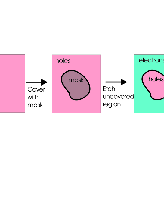
The advantage of this design is that by applying etch masks any shape of electron- and hole-sheets can be defined on the same wafer, as illustrated in Figure 1.
3 Modulation Doping
The main task in the design of the structure is to apply the modulation doping method by tuning parameters, such as bandgap, doping and dimensions. This section reviews modulation doping based on the book by Bastard [10].
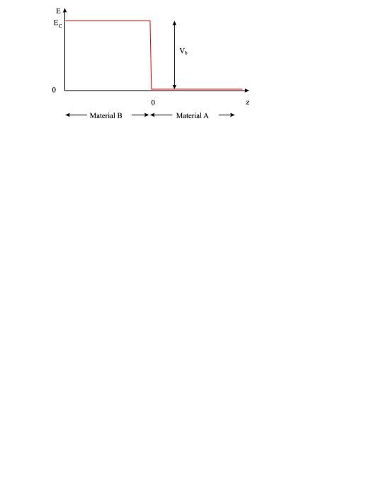
Consider an abrupt heterojunction between the two materials A and B, having different band gaps. A difference in two material bandgaps creates conduction and valence band discontinuities. Under flat-band conditions (unperturbed case) a possible conduction band profile is shown in Figure 2. Suppose material B contains impurities (for simplicity -type) and material A is intrinsic. One may regard an electron in the presence of a donor impurity of charge within the medium of the semiconductor, as a particle of charge and mass . This is precisely the problem of a hydrogen atom, except that the product of the nuclear and electronic charges must be replaced by -, and the free electron mass , by ([11], p.577 onwards). In almost all cases the binding energy of an electron to a donor impurity is small compared with the energy gap of the semiconductor.
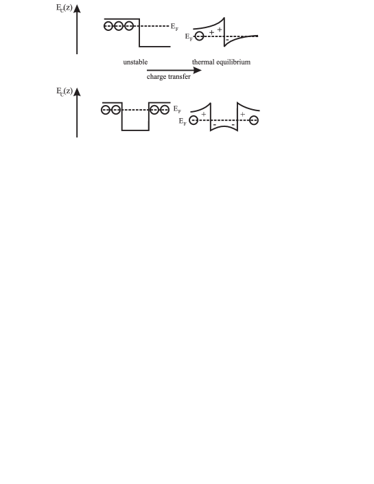
However, the electrons are bound relative to the conduction band edge of the B material. Therefore, their energies are above the onset of the heterojunction continuum. At the electrons would all be frozen on the impurity site but this situation is unstable since it does not ensure the equality of the Fermi level in both sides of the heterojunction. In material B it should lie between the donor levels and the conduction band edge, whereas in material A it should be negative since there are no free carriers.
To relax to thermal equilibrium, some of the carriers, assumed to be trapped at time onto the donor sites, tunnel or are emitted thermionically in the A material. By emitting phonons those electrons relax to (in a time scale of . The reverse process is unlikely, and in fact at impossible since no phonons are available to match the energy difference and tunnelling would correspond to the capture of an electron moving quickly in the layer plane, which is both inefficient and unlikely. Therefore, doping only the barrier acting material B, a spontaneous and irreversible charge transfer to the well acting material A is induced.
The spatial separation of electrons and their parent donors leads to band bending due to dipole formation between positively ionized donors and the electron on the other side of the heterojunction interface. This band bending only depends on , if one averages the donor distribution in the layer plane. This results in a quasi-triangular potential near the interface as shown in Figure 3, leading to bound states for the -motion. If the energy spacings are much larger than the thermal or collisional broadenings, the carrier motion becomes effectively quasi two-dimensional. One can repeat the reasoning with acceptor-doped barrier material: In this case the free carriers in the well-acting material are holes, which are bound and may form a quasi-two dimensional gas.
4 Asymmetric Modulation Doping
It is possible to replace Ga atoms in GaAs with Al to make the ternary material without any significant change in the electronic arrangement of the crystal lattice. At the same time the band gap changes from 1.43 eV (GaAs) up to 2.15 eV (temperature dependent). This material system is therefore suitable for implementing the modulation doping technique.
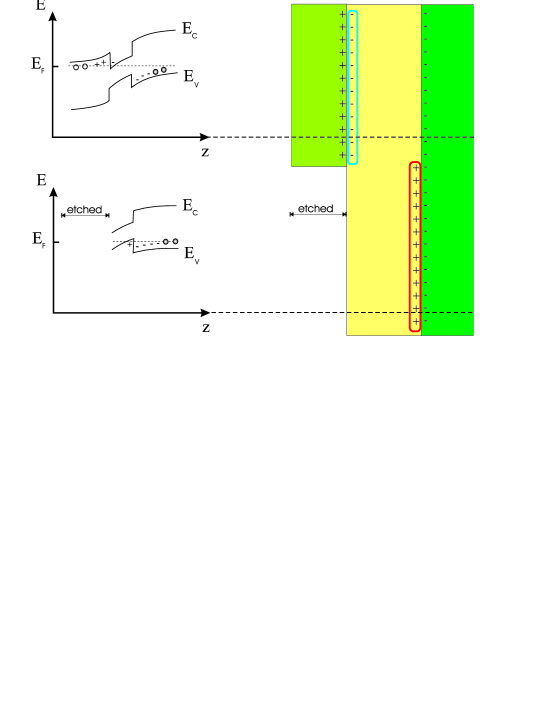
As explained above, in order to produce a lateral junction between electrons and holes, the low-bandgap material, which will be GaAs, is sandwiched between high bandgap material (AlxGa1-xAs) that on one side is acceptor and the other is donor doped. The situation is shown in the left part of Figure 4. For the diagram on top there are three possible cases: first, both, electrons and hole populate GaAs, secondly, only one type is present and thirdly, none. The desired case is the second one, where only one type of carrier is present, with the additional constraint that if the barrier-acting AlGaAs on one side is removed the other carrier type populates the GaAs material, as seen in the bottom diagram of Figure 4.
In this way, a junction between a two-dimensional electron gas, and a two-dimensional hole gas is produced at the edge between the regions where the top barrier-acting material has been removed. This is shown schematically in the right part of Figure 4.
5 Fermi-Level Pinning at the Surface
As indicated in the left part of Figure 4 the Fermi level at the left surface lies in the middle of the band gap. This pinning of the Fermi level at a fixed value (in this case at mid-gap) is caused by surface states. The closer the surface the heavier one has to dope the barrier-acting material in order to compensate for these surface effects. Therefore, Fermi-level pinning has to be taken into account when designing a structure like this.
The basic effect of cleaving and removing half of the crystal is to break bonds, which are left as singly occupied atomic orbitals known as dangling bonds. A monolayer of such bonds should form a two-dimensional energy band because of the translational symmetry along the surface. Those surface bands may lie, at least in part, in the forbidden energy gap. In this case one talks about surface states.
States in the forbidden gap will cause the Fermi level to change as one approaches the surface, in a way explained below. Clean, cleaved GaAs is free of surface states such that the position of the bulk bands with respect to the Fermi level is constant from inside the crystal all the way to the surface (p.488 [12]). This suggests that surface states do not necessarily arise for mechanical reasons. However, there is a chemical origin for GaAs surface states. This is revealed when cleaved GaAs is exposed to Oxygen. Photoelectron spectroscopy studies show that the surface Fermi level of GaAs (110) dosed with O2 is pinned for no more than 5% of oxygen surface coverage [13]. This revealed the appearance of elemental As at the surface [14, 13, 15, 16], suggesting that the GaAs was being chemically dissociated by the oxygen. This resulted in new electronic states (acceptors and donors) close to the exposed GaAs surface and within the bandgap.
The surface state density is generally quite high (/eV cm2) occurring at 0.4 to 0.5 eV above the valence band energy [17]. An -type doping producing electrons/cm3 leads to a carrier density at the surface of electrons/cm2. Hence, the Fermi level can only penetrate into the surface bands by an amount
This means that the Fermi level barely penetrates into the band of empty surface states. This is the origin of the phenomenon known as Fermi level pinning. It leads to the band bending displayed in the right diagram of Figure 4. This surface band bending results from the fact that in equilibrium the Fermi level must remain constant from bulk to surface: the band edges must then vary so as to be compatible with pinning at the surface and the bulk well away from it.
6 Wafer Design Based on a 1D Poisson Simulation
To predict which acceptor and donor densities and which channel width would result in a conducting lateral junction after the etch process the band-diagram as well as the charge density was simulated using a 1D Poisson solver [18]. It also takes quantized states into account, using the one-dimensional Schrödinger equation:
| (1) |
where is the wave function, is the total energy, the potential energy, is Planck’s constant divided by , and is the effective mass. The potential energy may be set to be equal to the conduction band energy .
For the AlGaAs system the conduction band and valence band effective masses, for electrons, light holes and heavy holes are given, respectively, in terms of the free electron mass kg by:
| (2) |
The wavefunction in (1) and the electron density are related by
| (3) |
where is the number of bound states, and is the electron occupation for each state. In general, the number of carriers in thermal equilibrium can be calculated from the density of levels in the conduction band and in the valence band at temperature by
| (4) | |||||
In the case of 2D quantized levels each sublevel has a constant density of states . The electron occupation for each sublevel can therefore be expressed by
| (5) |
where is the eigenenergy. The hole density can be calculated in a similar way, by setting the potential energy equal to the negative valence band energy .
In a quantum well of arbitrary potential energy profile, the spatial variation of is related to the electrostatic potential as follows:
| (6) |
where is the electrostatic potential and is the pseudopotential energy due to the band offset at the heterointerface. How the band gap difference of the regions 1 and 2 is distributed between the conduction and valence bands has a large impact on the charge transport in these heterodevices. The conduction band discontinuity is specified: . Knowing the band gap energies, the spatial variation of can also be derived. There are three primary conduction bands in the AlGaAs system that depending on the Al mole fraction , determine the bandgap. These are named , L and X. The default bandgaps for each of these conduction band valleys are as follows:
is the bandgap at K and set eV. The temperature dependence of the bandgap is calculated according to
| (7) |
where the constants are set as eV/K and K. is taken as the minimum of , , and .
The electrostatic potential can be derived from the charge carrier densities and via the one-dimensional Poisson equation
| (8) |
where is the dielectric constant, is the ionized donor concentration, and the ionized acceptor concentration. The static dielectric constant is -dependent, since it varies with the Al-mole fraction . For the AlGaAs-system it is given by
An iteration procedure is used to obtain self-consistent solutions for (1) and (8). Starting with a trial potential energy , the wave function, and their corresponding eigenenergies, can be used to calculate the carrier density distribution and using equations (3) and (5). Equation (8) can then be used to calculate . The new potential energy is then obtained from (6). The subsequent iteration will yield the final self-consistent solutions for , , and , which satisfy certain error criteria.
| No. | Material | Thickness in nm | Doping in cm-3 | remark |
|---|---|---|---|---|
| 1 | GaAs | 5 | capping layer | |
| 2 | Al0.5Ga0.5As | 10 | ||
| 3 | Al0.5Ga0.5As | 10 | ||
| 4 | Al0.5Ga0.5As | 2 | undoped | spacer layer |
| 5 | GaAs | 30 | undoped | conductive channel |
| 6 | Al0.4Ga0.6As | 3 | undoped | spacer layer |
| 7 | Al0.4Ga0.6As | 5 | ||
| 8 | Al0.4Ga0.6As | 20 | undoped | |
| 9 | Al0.3Ga0.7As | 300 | undoped | buffer layer |
| 10 | AlGaAs/GaAs | 500 | undoped | Superlattice |
| 11 | GaAs | - | undoped | Substrate |
This algorithm is now used to simulate the implementation of the lateral junction into the AlGaAs/GaAs material system. The temperature was assumed to be 4.2 K. A possible configuration is shown in Table 1. Several fabrication issues have been taken into account in the structure design already. Layer 1 is needed in order to protect the Al0.5Ga0.5As layer underneath from oxidizing. In addition, it was heavily doped which facilitates ohmic contact formation. The acceptor doping was chosen to be above the donor layers since the highly diffusive Beryllium was used as the acceptor dopant. Furthermore, the acceptor layers will have to be removed with high selectivity over the undoped GaAs layer (layer number 5). A selective etch exists which removes AlxGa1-xAs for over [19]. In order to achieve a high selectivity, the Aluminium content was chosen to be 50%.
The advantage of modulation doping, as far as impurity scattering is concerned, is the improvement in mobility due to the spatial separation between the carriers and their parent donors/acceptors. This spatial separation can be further enhanced by inserting a spacer layer, which is a nominally undoped part of the barrier, between the donor/acceptor and the 2DEG/2DHG. Therefore layers 4 and 6 have been inserted to act as spacer layers.
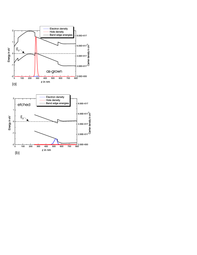
Figure 5 shows the simulated band diagram at 4.2 K of the etched and the as-grown wafer. The potential energy is normalized so that eV. Etching away layers 1 to 4 causes a significant change. In the as-grown state, lies well below the conduction band edge everywhere on the -axis. At the interface between layer 4 and 5 a sheet of holes is generated in the GaAs channel, as indicated by the red curve in Figure 5. This situation changes if the top 4 layers are removed. In this case lies above the valence band edge everywhere on the -axis. All free holes are depleted, but at the interface between layers 5 and 6 there is a formation of free electrons.
Even though the simulation of the structure does show the correct behavior, in reality varying activation levels of dopants in different growing chambers would require to start with a design which would allow for deviations from the simulation. A structure subject to optimization should at least be conductive and show carrier type alteration when etched. Other issues, such as parallel conduction and the actual vertical distance between the sheet of electrons and holes, should be considered after the device operation was demonstrated. The parameters of two possible wafer structures are shown in Table 2 and have been tested in [20, 21, 22].
| No. | Material | Thickness | Doping in cm-3 | |
| Wafer 2 | Wafer 1 | in nm | ||
| 1 | GaAs | GaAs | 5 | |
| 2 | Al0.5Ga0.5As | Al0.5Ga0.5As | 50 | |
| 3 | Al0.3Ga0.7As | Al0.5Ga0.5As | 3 | undoped |
| 4 | GaAs | GaAs | 90 | undoped |
| 5 | Al0.3Ga0.7As | Al0.3Ga0.7As | 5 | undoped |
| 6 | Al0.3Ga0.7As | Al0.3Ga0.7As | -doped cm-2 | |
| 7 | Al0.3Ga0.7As | Al0.3Ga0.7As | 300 | undoped |
| 8 | AlGaAs/GaAs SL | AlGaAs/GaAs SL | 500 | undoped |
| 9 | GaAs | GaAs | - | undoped |
Wafer 1 and 2 only differ in layer 3. This difference has the following two consequences. Firstly, the etch will remove Al0.5Ga0.5As, but not the thin Al0.3Ga0.7As layer, which was intended to passivate the surface and to cause un-pinning of the Fermi-level [23] (not observed). Secondly, the confinement at the interface between layer 2 and 3 will be stronger in the case of wafer 1, since the bandgap offset will be larger in this case.
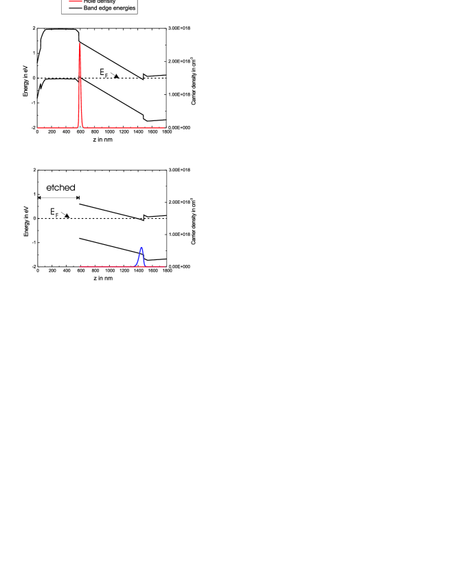
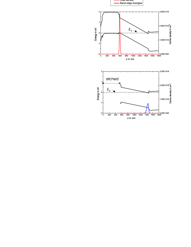
The donor doping (Silicon) was chosen to be delta-like in order to allow the implementation of multiple tunnel junction devices. As a consequence will be pinned at a deep donor level about 70 meV below the conduction band edge, even in the as-grown state. A narrow GaAs channel would therefore lead to very high electric fields, close to break down. Hence, the channel width was chosen to be 90nm, which is three times as large as in Table 1. There may be no need for using a -doped Si-layer and the channel can be made smaller.
A simulation of the band diagrams for both wafers is presented in Figure 6 and Figure 7. The electron and hole density is shown as blue and red curves, respectively. Depletion of the electrons is achieved by the increased confinement energy in the as-grown state as a result of the stronger electric field (steeper slope in and ) compared to the etched case. The change in charge carrier type, when the top layers are removed, can be seen in both cases.
The band-diagrams are limiting cases at a sufficiently large distance along from the junction. No information on the width of the junction can be obtained from the 1D Poisson simulation. The following chapter will investigate the transition region between these two limiting cases, i.e. the untreated and etched part of the wafer.
7 Two-Dimensional ATLAS Device Simulation
In order to obtain information on the transition between the band-diagrams in Figure 6 and Figure 7, the 2D Poisson solver from a device simulation package (ATLAS) from Silvaco International was used. A temperature of 300 K had to be assumed to ensure convergence of this program. However, the width of the junction should remain within the same order of magnitude.
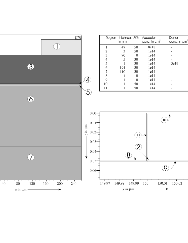
The real structure has to be brought into a format such that numerical calculations can be performed. First of all, an ideal sharp corner with vanishing radius is assumed at the step-edge. Also, in order to have as many mesh points as possible for the critical regions, the structure has only been simulated to a depth of about 450nm. Boundary conditions have been set, as described below to incorporate the effect of layers further down. A complete layer description can be found in Figure 8. For region 11 the layer thickness is measured in -direction, whereas for all other layers it will be in -direction. The acceptor doping in the real structure will diffuse into the -AlGaAs (region 2) and -GaAs (region 3) layer. Therefore the acceptor doping in the simulated structure was allowed to diffuse such that it drops according to a Gaussian function to half the original value after 1 nm.
As discussed above, the surface plays a crucial role in the electrical behavior, because it contains fixed charges that influence the carriers of the close-by conducting layers. In ATLAS these charges will be calculated directly from the surface states, instead of fixing as in the 1D simulation. Here, dangling bonds at the surface can be seen as a sheet of defects, whose associated energy may lie in the forbidden energy gap. These so called trap centers exchange charge with the conduction and valence band through the emission and recombination of electrons. Two possible states of these traps are assumed here: empty and full. When empty a trap has a particular cross-section for capturing an electron. It can either capture or emit an electron. When the charge on the trap has been changed by by the addition of an electron, it is full, and has a new cross-section for hole capture. Two basic types of trap have been found to exist: donor like (electron traps) and acceptor-like traps (hole traps). The charge contained within each type of trap will depend upon whether or not an electron or hole fills the trap.
A donor like trap is positively charged and therefore can only capture an electron. This means that donor-like traps are positive when empty of an electron but are neutral when filled. An acceptor trap is negatively charged so therefore they may only emit an electron. Therefore acceptor-like traps are negative when filled but are neutral when empty.
The probability of occupation assumed by ATLAS follows the analysis by Simmons and Taylor [24]. The probability of occupation is given by the following equations for donor- and acceptor-like traps, respectively:
where and are the thermal velocities for electrons and holes, and the electron and hole emission rates are given by:
| (9) |
where is the Boltzmann constant, is the intrinsic Fermi-level position and is the degeneracy factor of the trap center. and are the energy level of the donor trap measured from the valence band edge, and the energy level of the acceptor trap measured from the conduction band edge, respectively.
The surface is modelled by assuming a 1 nm thick layer of the corresponding bulk-material, containing both donor and acceptor-like traps. The corresponding parameters are:
| Region | in eV | in eV | in cm2 | in cm2 | in cm-3 |
|---|---|---|---|---|---|
| 8 | 0.7 | - | 10-8 | 10-9 | 10-20 |
| 8 | - | 0.7 | 10-9 | 10-8 | 10-20 |
| 10 | 0.9 | - | 10-8 | 10-9 | 10-20 |
| 10 | - | 0.9 | 10-9 | 10-8 | 10-20 |
| 11 | 0.9 | - | 10-8 | 10-9 | 10-20 |
| 11 | - | 0.9 | 10-9 | 10-8 | 10-20 |
Here measured from the and measured from are the energy level of the donor and acceptor trap, respectively.
Apart from the traps the surface regions do not contain any dopants. Region 11 has been added in order to have the flexibility to account for different characteristics for different surface orientations. Region 9 had to be included because otherwise problems with the automated mesh generation were encountered. However, this region is exactly the same as the underlying -GaAs layer. Region 8 and 10 do not contain traps directly underneath the ohmic contacts. Region 7 has been included at the bottom of the structure to pin the Fermi-level at 0.5 eV below the conduction band edge, the same value as obtained from 1D simulations.
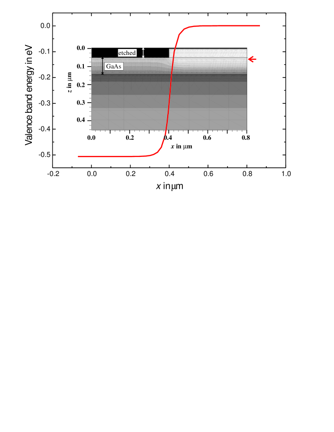
A two-dimensional plot of the valence band energy is shown in Figure 9. Light areas correspond to high values of . For m regions 1 and 2 were etched and therefore the GaAs channel appears darker. The junction width in direction was estimated by plotting the variation of over at the vertical height indicated by the red arrow. At this value the variation in is about eV, as it can be seen from the red curve, which is superimposed over the grayscale plot. The width of the junction is less than 80 nm. In [22] this value was verified experimentally.
8 Summary
The concept of carrier type alteration by selective etching was introduced. This method was then used to design a lateral junction between an electron and hole gas in a modulation doped AlGaAs/GaAs heterostructure. The issue of surface states in the design of this structure was discussed. A one-dimensional Poisson solver was used to simulate the banddiagram of various structures at 4.2 K, where carrier type alteration was predicted when the wafer was etched. The banddiagram in the transition region was modelled using a two-dimensional Poisson solver. Because of convergence problems the 2D simulation had to assume a temperature of 300 K. A junction width of less than 80 nm along the GaAs channel was predicted.
9 References
References
- [1] A. G. Aronov and G. E. Pikus. Spin injection into semiconductors. Sov. Phys. Semicond., 10(6):698, 1976.
- [2] R. Fiederling, M. Keim, G. Reuscher, W. Ossau, G. Schmidt, A. Waag, and L. W. Molenkamp. Injection and detection of a spin-polarized current in a light-emitting diode. Nature, 402:787, December 1999.
- [3] Y. Ohno, D. K. Young, B. Beschoten, F. Matsukura, H. Ohno, and D. D. Awschalom. Electrical spin injection in a ferromagnetic semiconductor heterostructure. Nature, 402:790, 1999.
- [4] H. J. Zhu, M. Ramsteiner, H. Kostial, M. Wassermeier, H.-P. Schönherr, and K. H. Ploog. Room-temperature spin injection from Fe into GaAs. Phys. Rev. Lett., 87:016601, 2001.
- [5] P. O. Vaccaro, H. Ohnishi, and K. Fujita. A light-emitting device using a lateral junction grown by molecular-beam epitaxy on GaAs (311) a-oriented substrates. Appl. Phys. Lett., 72(7):818, 1998.
- [6] B. Kaestner, D. G. Hasko, and D. A. Williams. Lateral p-n junction in modulation doped AlGaAs/GaAs. Jpn. J. Appl. Phys., 41:2513–2515, 2002.
- [7] Marco Cecchini, Vincenzo Piazza, Fabio Beltram, Marco Lazzarino, M. B. Ward, A. J. Shields, H. E. Beere, and D. A. Ritchie. High-performance planar light-emitting diodes. Appl. Phys. Lett., 82(4):636, 2003.
- [8] D. L. Miller. Lateral junction formation in gaas molecular beam epitaxy by crystal plane dependent doping. Appl. Phys. Lett., 47(12):1309, 1985.
- [9] T. Yamamoto, M. Inai, M. Hosoda, T. Takabe, and T. Watanabe. Demonstration of lateral p-n subband junctions in Si-delta-doped quantum-wells on (111)A patterned substrates. Jpn. J. Appl. Phys., 32(10):4454, 1993.
- [10] Gerald Bastard. Wave mechanics applied to semiconductor heterostructures. Monographies de Physique. Halsted Press, New York, 1988.
- [11] Neil W. Ashcroft and N. David Mermin. Solid State Physics. Saunders College Publishing, 1976.
- [12] P. Y. Yu and M. Cardona. Fundamentals of Semiconductors. Springer, Berlin, New York, 3rd edition, 2001.
- [13] W. E. Spicer, P. W. Chye, P. R. Skeath, C. Y. Su, and I. Lindau. New and united model for Schottky barrier and III-V insulator interface state formation. J. Vac. Sci. Technol. B, 16:1422, 1979.
- [14] C. D. Thurmond, G. P. Schwartz, G. W. Kammlotot, and B. Schwartz. J. Electrochem. Soc., 127:1366, 1980.
- [15] J. G. Ping and H. E. Ruda. The origin of Ga2O3 passivation for reconstructed GaAs(001) surfaces. J. Appl. Phys., 83:5880, 1998.
- [16] S. I. Yi, P. Kruse, M. Hale, and A. C. Kummela. Adsorption of atomic oxygen on GaAs(001)-(24) and the resulting surface structures. J. Chem. Phys., 114(7):3215, 2001.
- [17] H. Hasegawa and T. Sawada. Thin Solid Films, 103:119, 1983.
- [18] I.-H. Tan, G. L. Snider, L. D. Chang, and E. L. Hu. A self-consistent solution of Schrödinger-Poisson equations using a nonuniform mesh. J. Appl. Phys., 68(8):4071, 1990.
- [19] X. S. Wu, L. A. Coldren, and J. L. Merz. Selective etching characteristics of HF for . Electronics Letters, 21(13):558, 1985.
- [20] B. Kaestner, D. G. Hasko, and D. A. Williams. Quasi-lateral 2DEG-2DHG junction in AlGaAs/GaAs. Microelectronics Journal, 34(5-8):423, 2003.
- [21] B. Kaestner, D. A. Williams, and D. G. Hasko. Nanoscale lateral light emitting p-n junctions in algaas/gaas. Microelectronics Engineering, 67-8:797, 2003.
- [22] B. Kaestner, C. Schönjahn, and C. J. Humphreys. Mapping the potential within a nanoscale undoped gaas region using a scanning electron microscope. Appl.Phys.Lett., 84(12):2109, 2004.
- [23] P. A. Parikh, S. S. Shi, J. Ibettson, E. L. Hu, and U. K. Mishra. Hydrogeneration of GaAs MISFETs with Al2O3 as the gate insulator. Electr. Lett., 32(18):1724, 1996.
- [24] J. G. Simmons and G. W. Taylor. Nonequilibrium steady-state statistics and associated effects for insulators and semiconductors containing an arbitrary distribution of traps. Phys. Rev. B, 4:502, 1971.