Tunneling and nonlinear transport in a vertically coupled GaAs/AlGaAs double quantum wire system
Abstract
We report low-dimensional tunneling in an independently contacted vertically coupled quantum wire system. This nanostructure is fabricated in a high quality GaAs/AlGaAs parallel double quantum well heterostructure. Using a novel flip chip technique to align top and bottom split gates to form low-dimensional constrictions in each of the independently contacted quantum wells we explicitly control the subband occupation of the individual wires. In addition to the expected 2D-2D tunneling results, we have found additional tunneling features that are related to the 1D quantum wires.
pacs:
Valid PACS appear hereCoupled nanostructures show promise in leading to new understanding of non-fermi liquid physics, many-body effects and electron-electron interactions Zulicke2002 ; Eugster1991 ; Eugster1994 ; Smoliner1996 ; Ploner2000 ; Auslaender2002 ; Tserkovnyak2002 ; Bird2003 . The vertically coupled double quantum wire system described in this letter is a simple realization of such a coupled nanostructure. Proposals of coupled quantum wire devices that utilize tunneling and spin-orbit coupling to make a spin filter Governale2002 and coherent tunneling oscillations to form a qubit Bertoni2000 rely on exquisite control of the wire density, number of subbands occupied and coupling both between the wires and to the macroscopic environment.
In this letter we report tunneling measurements between vertically coupled double quantum wires fabricated using split gates on both sides of a double quantum well GaAs/AlGaAs heterostructure. While semiconductor based nanoelectronics promise a flexible platform, care must be taken that implementation of the quantum wires and the control over their subband occupation does not also alter the properties of the wires under investigation. With this issue in mind, we devise a tunneling geometry where the quantum wires are separated from the gates that are necessary for independent contacts. The price for this isolation is a 2D-2D tunneling component. We present tunneling results where 2D-2D resonances and additional structures are visible. The origin of the additional features and their relationship to 1D physics is investigated.
For the samples reported here, 18 nm wide GaAs quantum wells are separated with an AlGaAs barrier. For sample A the barrier is 7.5 nm and for sample B the barrier is 10 nm. The top and bottom quantum wells in sample B have individual layer densities of and cm-2 respectively and a combined mobility of cm2/Vs; sample A is similar. The heterostructure is thinned to approximately 0.4 m using an epoxy-bond-and-stop-etch (EBASE) process EBASE1996 . This allows for top and bottom split gates 150 nm from the top and bottom quantum wells, aligned laterally with sub-0.1 m resolution. The advantages of this device structure are three-fold. First, by making use of molecular beam epitaxy (MBE) growth of the tunneling barrier we have a rigid potential barrier between the layers. Second, the close proximity of the top and bottom split gates to the electron layers leads to a well-defined confinement potential for the 1D wires. Third, independent contact to individual electron layers in combination with the top and bottom split gates allows for the independent formation and control of the number of occupied subbands in both the top and bottom quantum wires.
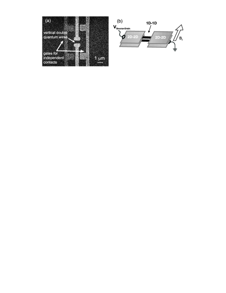
In Fig. 1(a), a top view scanning electron micrograph of a coupled quantum wire device is shown. The dark areas are the GaAs/AlGaAs heterostructure described above. The active region of the device consists of six TiAu gates. The four gates in the center form pairs of split gates defining the quantum wires. Only the two gates on the top surface are visible due to the accurate alignment of the top and bottom gates. The quantum wires are formed by electrostatic confinement in the 0.5 m wide and 1.0 m long gap between the split gates. The remaining two gates, spanning the entire field of view, are used to independently contact the individual electron layers. The lateral separation between the quantum wire and these gates is chosen to be 10 times greater than the depth of the quantum well to ensure a uniform density of the quantum wires. Low frequency measurements of the parallel transport and tunneling conductance are made using a standard ac method with a constant excitation voltage of 100 V at 13 to 143 Hz; dc IV’s are used as a consistency check. All measurements were taken at base temperature of a dilution refrigerator with an approximate electron temperature of 50 mK.
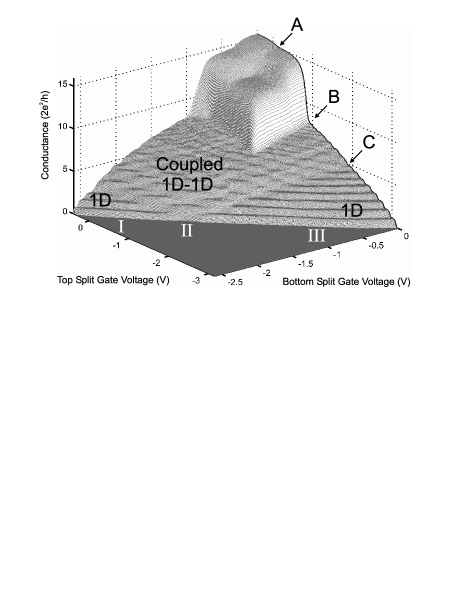
In Fig. 2 we plot the two-terminal linear conductance of the two layers in parallel as a function of the top and bottom split gate voltage for sample A. This figure shows the transition from 2D to 1D and finally to zero conductance as negative top and bottom split gate voltage is applied to the system. Consider the case where the bottom split gate voltage is fixed at zero and we vary the top split gate voltage. For top split gate voltages up to point A (Fig. 2 bold line) we have two 2D electron layers present. As we apply a larger negative top split gate voltage (-0.33 to -0.81 V, A to B) a wide 1D channel is formed in the top electron layer in parallel with the lower 2D layer. For larger negative top split gate voltage (-0.81 to -1.76 V, B to C) 1D constrictions form in each of the layers, although the top constriction is much narrower than the bottom constriction. By a top split gate voltage of -1.76 V (C) the top layer is completely completely depleted and conductance steps are observed in the bottom wire. The presence of quantized conductance in region III is an indication of the occupation of the bottom wire only. Similarly, in region I only the top wire is occupied. In the center region (II) of the figure we observe a more complicated pattern when both of the wires are occupied and contribute to the conductance. The complicated crossing pattern provides a means to map out the subband occupation and illustrates the control we have over the states of the individual wires.
A schematic view of the resonant tunneling geometry is shown in Fig. 1(b). Using this tunneling geometry we expect a combined 1D-1D and 2D-2D tunneling signal. The 1D-1D results from the overlap of the quantum wires themselves and the 2D-2D results from the small 2D areas on either side of the quantum wires. Resonant tunneling occurs when an electron in one wire tunnels to the other wire conserving both energy and momentum Zulicke2002 .
In Fig. 3(a) we show the 2D-2D ac tunneling conductance for several values of magnetic field, , applied parallel to the plane of the two-dimensional electron system and perpendicular to the tunneling current (see Fig. 1(b)). 2D-2D tunneling occurs when the top and bottom quantum wire split gates are grounded, while maintaining independent contact to the individual layers (see Fig, 1(a)). For 0 a sharp resonance occurs at 2.8 mV. We observe a decrease in the tunneling conductance and a splitting of the resonance with increasing magnetic field. This decrease and splitting has been previously observed Eisenstein1991 ; Smoliner1989 ; Smoliner1995 and is attributed to the magnetic field shifting the dispersion curves in k-space which reduces the phase space for tunneling and leads to a complex dependence on both the magnetic field and applied VSource-Drain (VSD). The observed 2D-2D tunneling at 2.8 mV is in good agreement with the measured densities of the two layers via Shubnikov-deHaas oscillations and gate depletion studies. Due to the presence of small 2D areas on either side of the quantum wires, the 2D-2D tunneling features described here are visible to some extent in all our tunneling results.
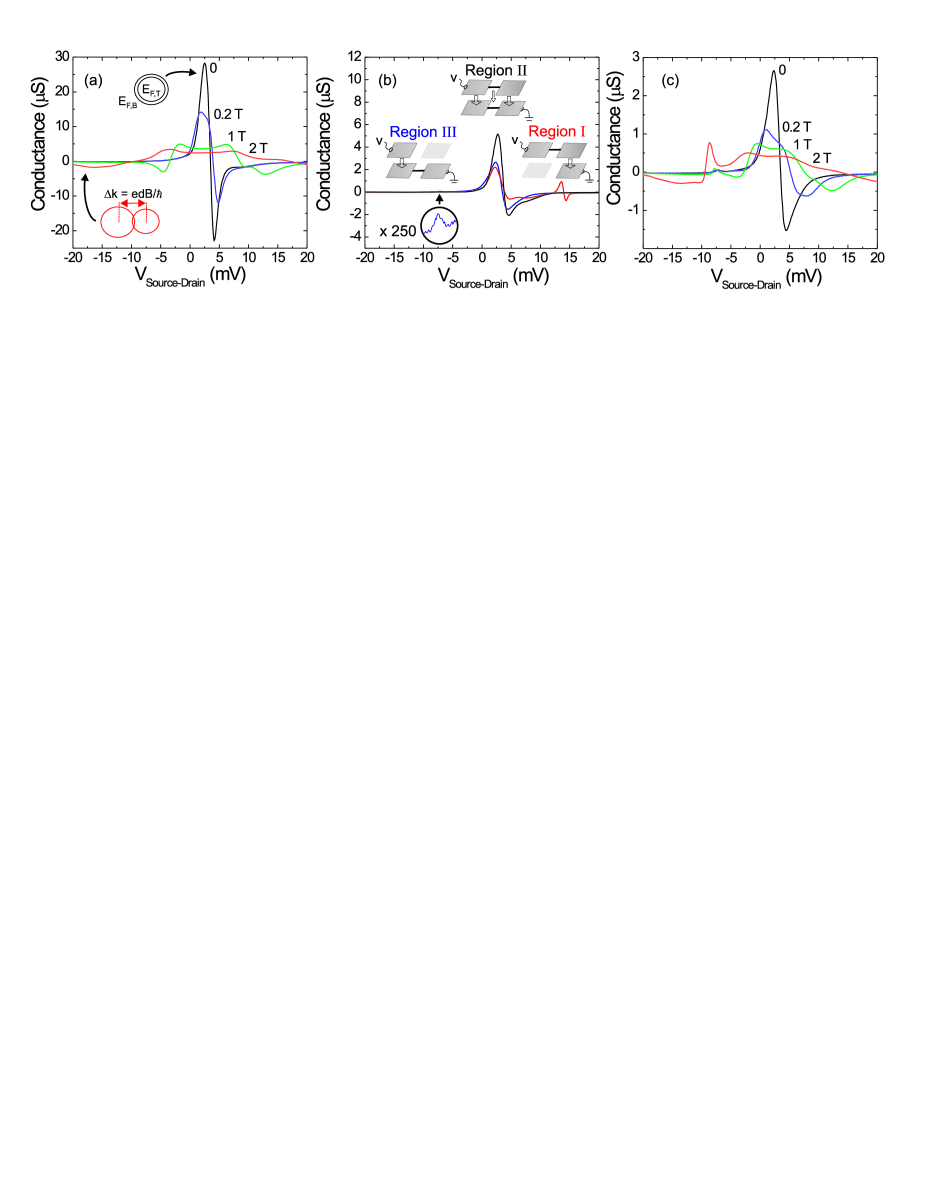
Fig. 3(b) shows the tunneling conductance in regions I, II and III for sample B with the top and bottom quantum wire split gates set to a parallel conductance of . The resonance at 2.8 mV is 2D-2D tunneling from the pair of 1 m 2 m 2D areas shown in Fig. 1. As we move from region I to region II we observe a doubling of the peak tunneling conductance. This is attributed to a doubling of the 2D-2D tunneling area as we move from only one wire occupied (region I) to both wires occupied (region II). The peak tunneling conductance is halved as we move from region II to region III for the same reason. An additional peak is observed at V 13 mV in region I and at V - 7 mV in region III enlarged view in Fig. 3(b). The position of these additional peaks are sensitively dependent on the top and bottom split gate voltage and are only visible when one of the wires is depleted. It should be noted that these additional peaks are not due to second 2D subband tunneling which occurs at 40 mV independent of the top and bottom split gate voltages. As we move towards region II the additional peaks move towards and collapse into the 2D-2D tunneling resonance. For a fixed top and bottom split gate voltage, the peak position is independent of magnetic field, but the amplitude can have a strong dependence as shown in Fig. 3(c).
In region II of Fig. 2 we have observed a 2D-2D tunneling signature as shown in Fig. 3(b). However, we have not observed a clear 1D-1D signal as expected. From previous work on vertically coupled quantum wires Tserkovnyak2002 we expect a 1D-1D conductance signal on the order of 0.01 S, which should be clearly observable in this experiment. Comparing 2D-2D tunneling results to the tunneling signal from region II we estimate that any 1D-1D signal buried in the 2D-2D background to be no larger than 0.001 S.
Finally we turn our attention to the side peaks in the tunneling when only one wire is occupied (regions I and III). From the strong magnetic field dependence of the amplitude (Fig. 3c) and the fact that the peak position in depends on the exact combination of top and bottom split gate voltages, it is tempting to conclude that the peak arises from 1D-2D tunneling. This tunneling could be from either the occupied or unoccupied wire to the 2D region in the other layer. If these features are indeed 1D-2D tunneling signatures, the tunneling process is quite different from the resonant 2D-2D tunneling. First, the insensitivity of peak position with suggests an inelastic origin. Second, we might expect each of the multiple 1D subbands to contribute additional tunneling channels; however, no other tunneling peaks are observed until the second 2D subband tunneling at 40 mV.
It is important to note the large values of the additional tunneling structures. Clearly nonlinear processes can be important. One example is lateral transport through the unoccupied wire at high bias. This could allow the floating 2D paddle (see diagrams in Fig. 3b) to contribute to tunneling. Finally, the effect of a depleted quantum wire at high bias is unknown in this system. While the origin of the additional tunneling peaks remains unknown, possibilities of 1D-2D tunneling and nonlinear transport are being explored to solve this important problem.
In conclusion, we have fabricated a nanoelectronic structure consisting of a pair of vertically coupled quantum wires and measured tunneling between the layers. The key to fabricating this device is the combination of EBASE thinning, electron beam lithography and depletion gates for separate contact. Transport measurements demonstrate external control over the number of occupied subbands in each 1D wire. With independent contacts, tunneling is measured between the quantum wire systems. An easily identified 2D-2D component is visible, and additional structure is present at high bias voltages when only one wire is occupied. The additional peak in the tunneling measurement is possibly related to 1D-2D tunneling or nonlinear transport of the unoccupied 1D wire. The successful combination of semiconductor heterostructures and dual-side electron beam lithography can be used to create a wide variety of electrically coupled nanostuctures for both fundamental and applied studies.
We thank S. K. Lyo for useful discussions and we acknowledge the outstanding technical assistance of R. Dunn and D. Tibbets. This work has been supported by the Division of Materials Sciences and Engineering, Office of Basic Energy Sciences, U.S. Department of Energy. Sandia is a multiprogram laboratory operated by Sandia Corporation, a Lockheed Martin Company, for the United States Department of Energy under contract DE-AC04-94AL85000.
References
- (1) U. Zulicke, Science 295, 810 (2002).
- (2) C. C. Eugster and J. A. del Alamo, Phys. Rev. Lett. 67, 3586 (1991);
- (3) C. C. Eugster, et al., Appl. Phys. Lett. 64, 3157 (1994);
- (4) J. Smoliner, Semicond. Sci. Technol. 11, 1 (1996).
- (5) G. Ploner, et al., Appl. Phys. Lett. 74, 1758 (1999);
- (6) O. M. Auslander, et al., Science 295, 825 (2002).
- (7) Y. Tserkovnyak, et al., Phys. Rev. Lett. 89, 136805 (2002); Phys. Rev. B 68, 125312 (2003).
- (8) T. Morimoto, et al., Appl. Phys. Lett. 82, 3952 (2003).
- (9) M. Governale, et al., Phys. Rev. B 65, R140403 (2002).
- (10) A. Bertoni, et al., Phys. Rev. Lett. 84, 5912 (2000).
- (11) M. V. Weckwerth, et al., Supperlatt. Microstruct. 20, 561 (1996).
- (12) J. P. Eisenstein, et al., Phys. Rev. B 44, 6511 (1991).
- (13) J. Smoliner, et al., Phys. Rev. Lett. 63, 2116 (1989).
- (14) G. Rainer, et al., Phys. Rev. B 51, 17642 (1995).