Giant Dielectric Permittivity of Electron-Doped Manganite Thin Films, Ca1-xLaxMnO3 ()
Abstract
A giant low-frequency, in-plane dielectric constant, , for epitaxial thin films of Ca1-xLaxMnO3 () was observed over a broad temperature range, 4K 300K. This phenomenon is attributed to an internal barrier-layer capacitor (IBLC) structure, with Schottky contacts between semiconducting grains. The room-temperature increases substantially with electron (La) doping, consistent with a simple model for IBLCs. The measured values of exceed those of conventional two-phase IBLC materials based on (Ba,Sr)TiO3 as well as recently discovered CaCu3Ti4O12 and (Li,Ti) doped NiO.
pacs:
77.22.Ch, 77.22.Gm, 77.55.+f, 77.84.BwI INTRODUCTION
High-permittivity dielectric materials play an important role in electroceramic devices such as capacitors and memories. Recent reports of giant permittivity have directed considerable attention to several new material systems: non-ferroelectric CaCu3Ti4O12,CCTO percolative BaTiO3-Ni composites,Percol and (Li,Ti)-doped NiO.NiO Of particular interest for applications is the weakly temperature dependent permittivity of these materials near room temperature. The enormous dielectric constant of these materials, , appears to beCCTOisIBLC a consequence of an internal barrier-layer capacitor (IBLC) structure, composed of insulating layers between semiconducting grains. IBLCs with effective based on (BaSr)TiO3 are well known,IBLCs but their usefulness is limited by a strong frequency and temperature dependence of their dielectric constant. Thus the newly discovered materials suggest that increases in values and/or simplification of processing could yield new and useful IBLC materials.
Here we report on giant values of the effective dielectric constant, , observed at low frequencies ( kHz) for thin films of the electron-doped manganite, Ca1-xLaxMnO3 (). The large and weakly - and -dependent near room temperature is attributed to an IBLC microstructure, comprising a network of depletion layers between semiconducting grains. is enhanced by electron doping via La substitution for Ca or oxygen reduction.
II EXPERIMENTAL METHODS
Polycrystalline targets of Ca1-xLaxMnO3 () were prepared by solid-state reaction as described previously.NeumeierCohn Powder x-ray diffraction revealed no secondary phases and iodometric titration, to measure the average Mn valance, indicated an oxygen content for all targets within the range 3.000.01. Thin films were grown by pulsed laser deposition using a 248 nm KrF excimer laser, with energy density J/cm2, pulse repetition rate 10 Hz, and target-substrate distance, 4 cm. The films were deposited on LaAlO3 (LAO) substrates of [100] orientation, with substrate temperature 750 ∘C and oxygen pressure 200 mTorr. Following the depositions, the chamber was filled to 700 Torr oxygen, held at 500 ∘C for 30 min., and subsequently cooled to room temperature. Film thicknesses were nm. X-ray diffraction (XRD) indicated epitaxial growth of the pseudocubic perovskite for all films, with lattice parameter, for CaMnO3. The full widths at half maximum of the (200) film reflections were typically 0.4∘. Scanning electron microscopy indicated an average grain size of 0.5-1m.
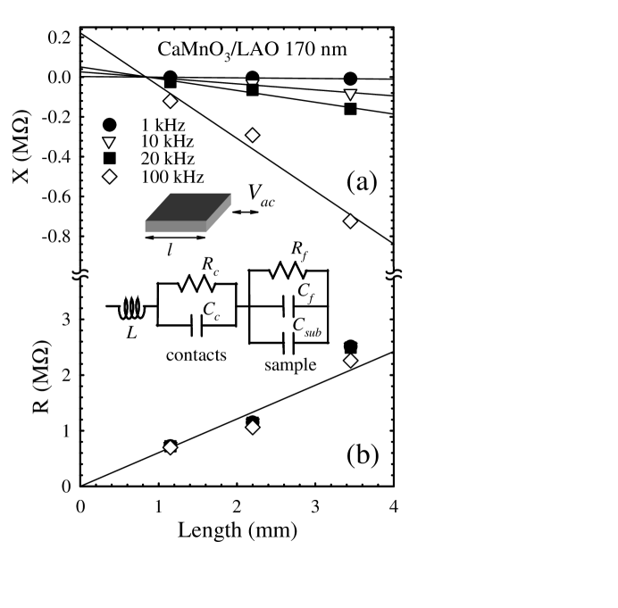
Impedance measurements were performed with a Hewlett-Packard model 4263B LCR meter in the frequency range 100Hz to 100kHz. A model HP16034E test fixture was used at room temperature, and a coaxial-lead, four-terminal pair arrangement in a cryostat for low temperatures. Silver paint electrodes, annealed at 300∘C, were applied on opposing edges of the specimens so that the ac voltage (0.2V for all measurements) was applied in the film plane. In this configuration, the film and substrate capacitances are additive; the equivalent circuit for contacts, film and substrate is shown in the inset of Fig. 1. A contact capacitance can lead to apparently large valuesLunkenheimerEprint of and thus great care is required to distinguish the true response of the sample. To address this issue, contact contributions to the impedance were eliminated at room temperature for some films by measuring the length dependence of the impedance (film+substrate), , on a series of films deposited simultaneously onto pre-cut substrates of different length, . Since the contact capacitance and resistance should be independent of , the measured reactance and resistance should be linear in , and , respectively. is a constant determined by a small serial inductance, (also assumed independent of ),NoteonInductance and the capacitive reactance of the contacts. These relations are followed well by the raw data (Fig. 1). The dielectric constant of the film was computed as,
| (1) |
where is the angular frequency of the applied voltage, () is the film (substrate) contact area and is the substrate dielectric constant. The latter, determined from a similar analysis of for blank substrates, was in good agreement with published values.SubstrateEps Uncertainty in determined from Eq. (1), arising principally from scatter in the data, was typically %. Values for determined from the length dependence analysis were consistently larger than those determined from direct measurements, indicating a predominance of the inductive reactance over the capacitive reactance of the contacts (i.e. ). The data presented below from direct measurements thus underestimate the true magnitude. The uncertainty in for the direct measurements near room temperature (where ) is given by that of the film thickness (). At the lowest temperatures, where , the uncertainty in is , largely due to a uncertainty in . For all measurements, the impedance was independent of ac voltage (50 mV-1 V) and applied DC bias (0-2 V).
III RESULTS AND DISCUSSION
The impedance of the target materials was measured in separate experiments. CaMnO3 is an antiferomagnetic (K) semiconductor with a small electron density associated with native defects, particularly oxygen vacancies, that yield a substantial room temperature conductivity, m-1. Electron doping via La substitution for Ca further enhances , especially at low .NeumeierCohn could be determined reliably only at K where the capacitive reactance was sufficiently large (). was describable as a sum of a constant term (the high-frequency and lattice terms) and a dipolar contribution associated with hopping charge carriers.Jonscher The latter gives rise to steps in which occur at lower with decreasing frequency, as shown for CaMnO3 in Fig. 2 (a) (solid curves). This indicates a relaxation process associated with thermal activation of localized charge carriers, characterized by a relaxation time, . Analyzing the maxima in (corresponding to ) we find meV and s. These parameters are typical of polaronic relaxation in LaMnO3Lunkenheimer and other perovskites.Bidault For comparison, meV, s were reported for single-crystal CaCu3Ti4O12,Homes and meV, s for (Li,Ti)-doped NiO.NiO Relevant to the subsequent discussion of films, it was found that increasing the electron density, either through oxygen reduction or La doping, resulted in a decrease (increase) in . Further details of measurements on the polycrystalline bulk materials will be presented elsewhere.CohnUnpub
Figure 2 (a) shows at three frequencies ( kHz) for a 170-nm film of CaMnO3. The inset shows at room temperature for a second piece of the same film measured to 100 kHz. At low temperatures, has a magnitude comparable to the bulk material and small steps occur at temperatures similar to those at which the bulk material exhibits dipolar relaxation. With increasing temperature a second dispersive step is observed near 200 K, with increasing by an order of magnitude. For K, with weak temperature and frequency dependencies. Both steps in appear as maxima in the dielectric loss [, Fig. 2 (b)]. The appearance of the high-temperature step is typical of IBLC materials where insulating barriers separate semiconducting grain interiors. Such a system can be modelled as two circuits in series, one for the grain interiors and one for the grain-boundary response.CCTOisIBLC The grain-boundary time constant, , gives rise to a second relaxation process that is thermally activated via the behavior of . From the temperatures of the maxima in measured for two pieces of this film we compute [inset, Fig. 2 (b)] average values for activation energies meV and s [( s] for the grain interior [grain-boundary] relaxations. The values of and inferred for the grain interiors are significantly smaller and larger, respectively, than the corresponding values determined for the targets. This indicates that the grains of the film are more oxygen deficient, and suggests oxygen is lost during deposition. Consistent with this conclusion, the films haveCohnUnpub K in accord with magnetic measurements on oxygen deficient, bulk CaMnO3-δ.Briatico
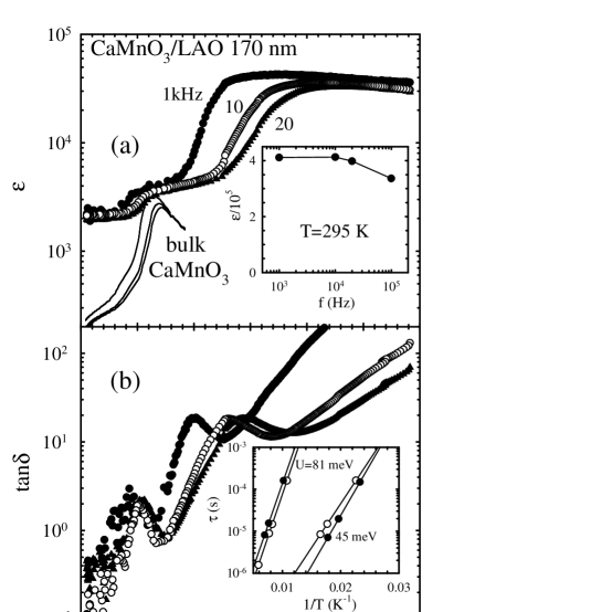
Figure 3 shows and for a 55-nm film grown from a Ca.97La0.03MnO3 target. The qualitative features of the data for the as-prepared specimen (open symbols) are similar to that of the CaMnO3 film except that is substantially larger, at 300 K and the lower temperature step in is absent. The higher carrier density of the La-doped material suppresses the carrier freeze-out responsible for the low- relaxation to temperatures below our measurement range.CohnUnpub A greater dc conductivity is responsible for the sharp increase of at higher temperatures. The grain-boundary relaxation is evident as weak maxima or plateaus in . Analysis of the relaxation yields, meV and s.
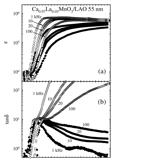
After sitting in ambient conditions for three months, at 300 K for the same specimen (solid symbols) decreased by %, but had decreased dramatically; by more than four orders of magnitude at 1 kHz and nearly two orders of magnitude at 100 kHz (Fig. 3). At lower temperatures, exhibits well-defined maxima, and below these maxima matches the data in the as-prepared state. Thus much of the loss near room temperature in the as-prepared films is associated with dc conduction that is substantially suppressed with “aging”.
As for other IBLCs composed of compound semiconductors, our data can be understood by considering the films to be random arrays of close-packed, electrically-active semiconducting grains. Boundaries between grains contain an interface charge , and are adequately described as double Schottky barriersGreuterBlatter with capacitance, , where is the area of contact between grains, is the bulk semiconductor dielectric constant, is the depletion layer width on either side of the grain boundary (assumed symmetric), and is the donor density in the bulk semiconducting grains. Since the grain diameter is typically , the “brickwork” modelIBLCs can be applied to the array of grains, such that the effective dielectric constant is given approximately as, .
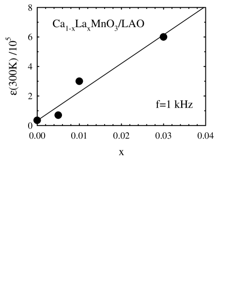
With increased electron (La) doping, for the films increases considerably (Fig. 4). This data allows for a test of the simple model above. Reasonably assuming that the oxygen vacancy concentration () for the films is independent of , we compute the slope, , by making the substitution ,
| (2) |
where is the volume per formula unit.Ling The line in Fig. 4 yields . Using (Fig. 2 and Ref. CohnUnpub, ) and (from scanning electron microscopy), we compute an interface charge density of . This value is typical of those found for a variety of compound semiconductors.GreuterBlatter That is approximately linear in implies that variations in and with doping are either negligible or cancel.
The aging effect in the films is most likely associated with oxidation at grain surfaces. This hypothesis is supported by preliminary oxygen annealing studies on a 55 nm CMO film. was reduced by a factor of two with no measurable change in following a 15-hour, flowing-oxygen anneal at 700∘C. A small decrease in for aged films is consistent with a small increase in .
Finally, we note that the large values of reported here are not limited to manganite films with compositions near 100% Ca. We have measured at room temperature for a 55 nm film grown under identical conditions from a La0.7Ca0.3MnO3 target (a colossal magnetoresistance composition). Films of other insulating compositions with the appropriate microstructure may also possess a large effective .
IV CONCLUSIONS
In summary, thin films of Ca1-xLaxMnO3 (00.03) have been found to exhibit giant low-frequency dielectric constants, , that are weakly temperature and frequency dependent near room temperature. These enormous values are attributed to a barrier-layer capacitor microstructure produced during deposition and subsequent exposure to air by oxidation of grain boundary regions which form an insulating shell on semiconducting grains. increases with charge-carrier doping, consistent with a reduction in the depletion-layer width at grain boundary contacts and a nearly doping-independent surface charge. Though lower dielectric losses will be required for applications ( is desirable), the considerable reduction of upon aging or oxygen annealing with little decrease in motivates further investigations of processing conditions.
ACKNOWLEDGMENTS
The authors gratefully acknowledge experimental assistance from Dr. B. Zawilski. The work at the Univ. of Miami was supported, in part, by NSF Grant No.’s DMR-9504213 and DMR-0072276, and at Montana State Univ. by Grant No. DMR-0301166.
† present address: Physics Department, University of Pennsylvania, Philadelphia, PA
References
- (1) M. A. Subramanian et al., J. Solid St. Chem. 151 232 (2000); A. P. Ramirez et al., Sol. St. Commun. 115, 217 (2000).
- (2) C. Pecharromán et al., Adv. Mater. 13, 1541 (2001).
- (3) J. Wu et al., Phys. Rev. Lett. 89, 217601 (2002).
- (4) D. C. Sinclair et al., Appl. Phys. Lett. 80, 2153 (2002).
- (5) C.-F. Yang, Jpn. J. Appl. Phys. 36 188 (1997).
- (6) J. J. Neumeier and J. L. Cohn, Phys. Rev. B 61, 14319 (2000).
- (7) A. K. Jonscher, Dielectric Relaxation in Solids, (Chelsea Dielectrics Press, London, 1983).
- (8) P. Lunkenheimer et al., Phys. Rev. B 66, 052105 (2002).
- (9) Any inductance from the film would be expected to scale with , tending to reduce the value of in Eq. (1); since , the computed dielectric constant represents a lower bound.
- (10) see, e.g., Handbook of Thin Film Devices, ed. by M. H. Francombe, (Academic, New York, 2000), Vol. 3, Ch. 1, p. 19.
- (11) A. Seeger et al., J. Phys. Cond. Mat. 11, 3273 (1999).
- (12) O. Bidault et al., Phys. Rev. B 52, 4191 (1995).
- (13) C. C. Homes et al., Science 293, 673 (2001).
- (14) J. L. Cohn, M. Peterca, and J. J. Neumeier, Phys. Rev. B, in press (cond-mat/0410657).
- (15) J. Briatico et al. Phys. Rev. B 53, 14020 (1996).
- (16) F. Greuter and G. Blatter, Semicond. Sci. Technol. 5, 111 (1990).
- (17) C. D. Ling et al., Phys. Rev. B 68, 134439/1-8 (2003).