Energetics of intrinsic point defects in ZrSiO4
Abstract
Using first principles calculations we have studied the formation energies, electron and hole affinities, and electronic levels of intrinsic point defects in zircon. The atomic structures of charged interstitials, vacancies, Frenkel pairs and anti-site defects are obtained. The limit of high concentration of point defects, relevant for the use of this material in nuclear waste immobilization, was studied with a variable lattice relaxation that can simulate the swelling induced by radiation damage. The limit of low concentration of defects is simulated with larger cells and fixed lattice parameters. Using known band offset values at the interface of zircon with silicon, we analyze the foreseeable effect of the defects on the electronic properties of zircon used as gate in metal-oxide-semiconductor devices.
pacs:
71.15.-m,71.15.Nc,79.20.Ap,61.80.-x,34.20.CfI Introduction
Its ability to accommodate actinides, its high resistance to corrosion and low thermal conductivity makes zircon a candidate ceramic for immobilization of nuclear wasteet. al. (1998); Ewing et al. (1995). The effect of radiation damage in these ceramics has to be studied in order to control possible leaching, creep and fatigue in the material. In radiation damaged samples, an anisotropic volume swelling of up to 5% was observed in the crystalline phase. When the damage is not too large, there is a coexistence between amorphous domains and the crystalline phase. The former is due to collision cascades caused by the recoil particles, while the -particles produce point defects in the remaining crystalline phase. X-ray diffraction experiments show that this crystalline phase expands by up to 1.5% along the ab-axis, and 2% along the c-axisHolland and Gottfried (1955). It is known that high concentrations of point defects strongly affect the structural properties of crystalline zirconRíos et al. (2000). The accumulation of charged defects produce electric fields that would also change the kinetics of accumulation and diffusivity.
In a different context, the high dielectric permittivity of zircon has recently generated considerable interest in the electronic industry. The reduction of the size of metal-oxide-semiconductor transistors requires the use of a gate dielectric with high electric permittivity (high-) in order to avoid the leakage, coming from direct tunnelling of carriers through the potential barrier of the insulator. Alternatives to SiO2 are being sought. Oxides and silicates of transition metals such as Zr and Hf have been stabilised in contact with Si up to high temperatures. The silicates are specially promising because they form an interface with the silicon that is chemically similar to the SiO2-Si interfaceWilk and Wallace (2000). The permittivity of amorphous ZrSixOy silicates increases as the concentration of Zr increases, but it also reduces the band gap of the material. This reduction of the insulator band gap degrades the potential barrier for tunnelling, therefore increasing the leakage. Low concentrations of point defects can affect the electrical properties of the material, and hence have a significant role in the performance of zircon as a gate dielectric. Electron and hole trapping by defects may change the electronic structure in the band gap, and affect the leakage current.
The importance of zircon for nuclear waste immobilization, where defect accumulation in radiation-damaged samples affects the crystalline structure, and as an alternative gate dielectric, where low concentrations of defects can affect the device performance, motivates the study of both the high concentration and the low concentration limits. Previous theoretical studies of point defects in zircon were focused on the structural properties, and on energetics of the neutral defects, showing that oxygen interstitial is the most stable one, with a non negligible concentration expected at thermal equilibriumCrocombette (1999). In the present work, we use first principles electronic structure calculations to study the influence of a variety neutral and charged point defects on the electronic structure of ZrSiO4. The formation energies will depend on the chemical environment, and can be obtained as a function of the chemical potentials of the electrons and of the atomic species present in the system. The electron and hole affinities, and the ionization energies are important parameters that determine the charge state of the defect, and the capacity of trapping electrons (or holes) in the interface with silicon in electronic devices.
II Method
II.1 Details of the calculations
Zircon (ZrSiO4) crystallises in the tetragonal space group. The structure consists of alternating SiO4 tetrahedra and ZrO8 triangular dodecadeltahedra edge-sharing and forming chains parallel to the crystallographic axis. A body-centred unit cell can be chosen, containing four formula units. The structure is fully described with four parameters (see Table 1): the lattice constants and , and the internal parameters and that define the positions of oxygen atoms in the sites. Calculations of the electronic properties of ZrSiO4 are performed with the self-consistent ab initio siesta method,Ordejón et al. (1996); Soler et al. (2002) using Density Functional Theory (DFT)Hohenberg and Kohn (1964); Kohn and Sham (1965) within the Local Density Approximation (LDA)Ceperley and Alder (1980) and separable norm-conserving pseudopotentials.Troullier and Martins (1991); Kleinman and Bylander (1982) The valence wave functions are expanded in linear combinations of strictly localized pseudoatomic numerical orbitalsJunquera et al. (2001). Technical details of the pseudopotentials and the basis set used are described in reference Pruneda et al., 2004. The relaxed parameters calculated for bulk zircon are in good agreement with experimental values (Table 1).
| This work | Ref. [Rignanese et al., 2001] | Expt. [Robinson et al., 1971] | |
|---|---|---|---|
| Volume | |||
| (Å3) | 129 | 127 | 131 |
| Lattice parameters | |||
| (Å) | 6.59 | 6.54 | 6.61 |
| (Å) | 5.96 | 5.92 | 5.98 |
| 0.068 | 0.064 | 0.066 | |
| 0.184 | 0.194 | 0.195 | |
| Interatomic distances | |||
| Si-O (Å) | 1.625 | 1.61 | 1.622 |
| Zr-O (Å) | 2.125 | 2.10 | 2.131 |
| 2.247 | 2.24 | 2.268 | |
| Zr-Si(Å) | 2.979 | 2.991 | |
| 3.617 | 3.626 | ||
| Bond angles | |||
| O-Si-O | 96.16o | 97o | 97.0o |
| O-Si-O | 116.50o | 116o | 116.06o |
To simulate the defect structures, the host crystal is represented by a supercell generated by repetition of the conventional unit cell (4 formula units). The point defects are then introduced inside this supercell (adding atoms for interstitials, removing atoms for vacancies, etc), that have to be large enough to describe the sought defect concentrations. We use host supercells with 24, 48, 96, and 192 atoms. The supercell with 48 atoms is a 112 (repetition of the tetragonal cell along the axis), the one with 96 is a 221 (repetition along the and axis), and the one with 192 is a cell 222. In this way, different concentrations of defects can be simulated by changing the number of repetitions in the cell. The unphysical divergence in the energy coming from the long range Coulomb interactions of a periodicly repeated charged defect, is compensated by a uniform electron-charge neutralising background. Makov and Payne (1995) In ref.[Pruneda et al., 2004] we studied the effect of high concentrations of intrinsic point defects in the structure of zircon and we allowed for lattice relaxation of the supercells. The resulting lattice parameters are used to simulate the limit of high concentration of defects. On the other side, the 192 supercell with the lattice parameters of the perfect crystal structure is used for studying the electronic properties at low concentrations (isolated defects).
II.2 Defect formation energies
The formation energy of a defect in charge state is a function of both the electron chemical potential , and the chemical potentials of the species involved in the defect:
| (1) |
In this expression, represents the energy of the defective supercell containing atoms of species with chemical potential , at T=0 (we neglect entropic contributions). The Fermi level is measured relative to the top of the valence band, . This valence-band top may be shifted from the bulk value when a charged defect is introduced, because the potential in periodic boundary conditions is determined only up to a constant. To compare energies the band structures of the perfect and defective supercells have to be lined up. We take this shift to be given by the difference in the potential far away from the defect in the defect cell and in the bulk system. Laks et al. (1992)
When the formation energies of different defects are compared, it
should be done as a function of the chemical potentials and Fermi
level. The chemical potential for each element is specified by a
reference state, and it is then assumed that there is a thermodynamic
equilibrium between the reference system (that acts as the reservoir
of atoms where the interstitials come from and where atoms go to)
and the zircon crystal.
There are some thermodynamic limits to the chemical potentials: if
we take the values of bulk silicon and zirconium, and the
molecular form of oxygen as origin for our chemical potentials, then
{} are bound by:
(i) the values that make ZrSiO4 stable,
| (2) |
(ii) the values that cause precipitation of its constituents,
| (3) |
(iii) and the values that cause formation of the oxides:
| (4) | |||
| (5) |
where is the generalised formation free energy of the corresponding solid compound relative to bulk silicon, bulk zirconium and molecular oxygen (see table 2).
| Constituents | This work | Expt. |
|---|---|---|
| Zr + O2 ZrO2 | -12.1 | -11.5Fiorentini and Gulleri (2002) |
| Si + O2 SiO2 | -9.6 | -9.8Jr. (1998) |
| Zr + Si + 2O2 ZrSiO4 | -22.3 | -20.9Jr. (1998) |
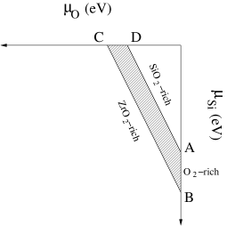
Relation (2) can be used to reduce the dependence of the defect formation energy on just a pair of atomic chemical potentials. Choosing we would have the “stability quadrangle” shown in figure 1, where relations (4) and (5) determine the ZrO2-rich and SiO2-rich environments, and the shaded region corresponds to values of that satisfy all the conditions (2-5). Notice that for the study of ZrSiO4 thin films grown over silicon, this particular choice is more convenient than or .
The Fermi level, is bound between the valence-band top, and the conduction-band bottom.
| (6) |
The band gap, , can be calculated as the difference of the energies of the system with N1, N, and N1 electronsPantelides et al. (1974):
| (8) | |||||
In this way, we obtain that the band gap is 5.12 eV (it can be compared with the value of 4.91 eV obtained from the calculated electronic band structure). The experimental value is about 6.0 eVRobertson (2000), but is well known that DFT (GGA and also LDA) underestimates . The difference () between theoretical and experimental gap is the main source of inaccuracy for the defect levels.
II.3 Energy Levels
The positions of the defect levels with respect to the bottom of the conduction band are useful for the study of photo-stimulated and thermo-stimulated processes. The electron (hole) affinity, [], is defined as the energy gained when a free electron (hole) from the bottom of the conduction band (top of the valence band) is trapped at the defect. It is computed by comparing energies of systems with the same number of electrons. The difference between the experimental and theoretical energy gap can be used to correct the electron affinity Foster et al. (2002),
| (9) |
| (10) | |||||
With these definitions, we have that We will consider the relaxed electron and hole affinities, that include the lattice relaxation after the electron/hole trapping. This method is approximate and the main source of errors come from the underestimated band gap in DFT calculations.
The defect transition energy defined asZhang et al. (2001)
| (11) |
determines the energy required to change the charge state of a defect from to . The charge state of the defect will be if the Fermi level is below , and will be if is above .
III Results
We have considered a variety of neutral and charged intrinsic defects, including interstitials (Xi) and vacancies (VX) of the three elements (Si,O,Zr) present in zircon, Zr and Si anti-site defects (Zr, and Si), Frenkel pairs (X), and other combinations of interstitials and vacancies. The description of the structures of these defects is given in Ref. [Pruneda et al., 2004] for the high concentration limit, and are essentially the same for the diluted case.
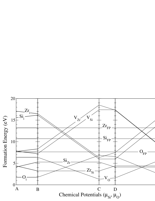
The presence of high concentration of point defects in zircon produces a strong modification of the lattice parameters. The most important distortions are produced by interstitials of Si and Zr, and for the antisite Zr. For these defects, we reportedPruneda et al. (2004) variations in the lattice constants of the order of 1.5% for the limit of high concentration studied (defects/cm3). Figure 2 shows the energies as a function of and , along the directions defined in Fig.1. According to this figure, interstitials and vacancies of oxygen, and the antisite Zr are stable defects over a broad range of chemical potentials, followed by the Si antisite. The energies for incorporation of native neutral point defects in ZrSiO4 are presented in table LABEL:energy, with the reference for the chemical potentials given in the A point. We consider that this particular position, corresponding to an O2-rich and SiO2-rich environment is appropriate to describe formation energies for both zircon thin-films grown on silicon, and for the crystalline phase of radiation-damaged samples. In the latter, molecular dynamic simulations Trachenko et al. (2002) show that the content of oxygen in the cascade regions is reduced, becoming a source of oxygen for the crystalline regions. Traces of polymerisation observed in nuclear magnetic resonance experiments Farnan and Salje (2001), tend to indicate that the formation of SiO2-rich domains is favorable in damaged samples.
The lattice distortion induced by the high concentration of defects discussed previously does not substantially affect the formation energies, as can be observed by the fact that the values obtained for the undistorted 2x2x2 supercell (192 atoms) are very similar to the formation energies of the same defects in the distorted 1x1x2 supercell (48 atoms) shown in table LABEL:energy. The small interaction between defect images is also reflected in the similarity of these energies.
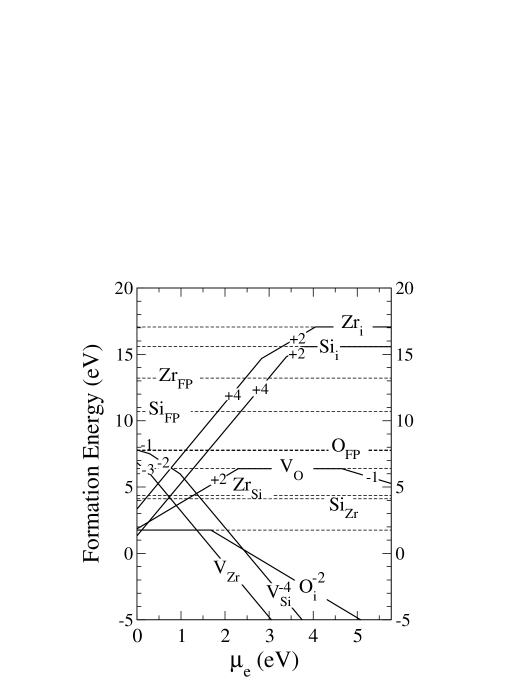
Figure 3 shows the formation energies as a function of the electronic chemical potential for the atomic chemical potentials given by the point A. For values of not too close to the bottom of the conduction band, cation interstitials are more stable in positively-charged configurations. Cation vacancies prefer negatively-charged states, and the same is true for the oxygen interstitial when is 2 eV above the top of the valence band. In the following, we will discuss the energetic properties of each family of defects.
| Defect | 24 | 48 | 96 | 192 | Ref. [Crocombette, 1999] |
|---|---|---|---|---|---|
| Oi | 1.7 | 1.7 | 2.0 | 1.1 | 1.7 |
| Sii | 14.5 | 15.6 | 15.5 | 16.4 | 17.0 |
| Zri | 17.1 | 17.6 | 15.9 | 18.0 | |
| V | 6.3 | 6.4 | 6.5 | 6.9 | 5.6 |
| V | 3.6 | 7.8 | 8.5 | 5.8 | |
| V | 7.4 | 7.7 | 7.9 | 5.9 | |
| O | 7.6 | 7.3 | |||
| Si | 10.7 | 22.9 | |||
| Zr | 13.2 | 24.0 | |||
| Si | 4.1 | ||||
| Zr | 4.1 | 4.4 | 3.0 |
III.0.1 Oxygen related defects
The neutral interstitial oxygen forms a “dumbbell” structure with another oxygen atom in the latticeCrocombette (1999); Pruneda et al. (2004), an arrangement also observed in ZrO2. The structure of charged O does not differ substantially from the neutral defect, but in the doubly charged state the oxygen displaces from the dumbbell structure, and forms a bridge between neighbour silicon atoms, both becoming fivefold coordinated. Pruneda et al. (2004) The relaxation energy from the initial dumbbell configuration is of about 1.6 eV. The energy of the neutral defect in the atomic structure of O is 2.9 eV higher in energy. This lowering of the energy that results from the capture of a second electron is known as Anderson’s “negative-U” behaviour. Anderson (1975) It is interesting to note that the decay of two isolated O centre into a O and a neutral Oi is energetically favorable, with a gain of 0.4 eV (see table 4).
In the V, the silicon atom moves slightly towards the missing oxygen in its tetrahedron, and the remaining Si-O bond lengths are increased by 4%. In the charged defect V, the Si atom moves back towards its initial position. The Si-O bonds have deviations smaller than 1% with respect to the original Si-O tetrahedra. Again, there is a negative-U behaviour, and the decay reaction 2VVVO releases an energy of 1.7 eV.
In the case of O, the interstitial and the vacancy do not interact strongly, and the final configuration is similar to a pair of isolated vacancy and dumbbell interstitial (E(Oi)+E(V)=8.2 eV for the supercell with 48 atoms), even when both are in the same original Si-O tetrahedra. The energy of the charged pairs (computed from the energies of isolated charged interstitial and vacancy) is slightly different, with VO 0.5 eV higher in energy, and VO 1.2 eV lower than the neutral pair, showing a tendency towards charge transfer between oxygen vacancies and interstitials.
| Energy (eV) | ||||
|---|---|---|---|---|
| Reaction | high-C | low-C | ||
| O + O | O | |||
| V + V | V | |||
| O + V | O +V | |||
| O + V | O +V | |||
| O + V | O +V | |||
| Si + Si | Si | |||
| Si + Si | Si | |||
| Si + Si | Si | |||
| V + V | V | |||
| V + V | V | |||
| Si + V | Si +V | |||
| Si + V | Si +V | |||
| Si + V | Si +V | |||
| Si + V | Si +V | |||
| Zr + Zr | Zr | |||
| Zr + Zr | Zr | |||
| Zr + Zr | Zr | |||
| V + V | V | |||
| V + V | V | |||
| Zr + V | Zr +V | |||
| Zr + V | Zr +V | |||
| Zr + V | Zr +V | |||
| Zr + V | Zr +V | |||
III.0.2 Cation related defects
Neutral interstitials of Zr (Si) are relatively stable in a Zr-rich (Si-rich) environment, but in general have higher formation energies. These defects are more likely to exist in their charged states X or X (with X=Zr or Si) than in the neutral state, depending in the position of the Fermi level (figure 3 and table 4). Upon removal of electrons from Sii, new atomic structures are obtained, with the interstitial making oxygen atoms to approach, and neutralize the charge around it. The geometries for positively charged Zr-interstitials are basically unchanged with respect to the neutral structure. The combination of neutral isolated vacancies with interstitials would favour a charge transfer between them. In that case, there is a strong ionic interaction between interstitial and vacancy and a clear trend towards defect annihilation. This results in relatively high formation energies for Frenkel pairs of Zr and Si. Our values for the formation energies in these defects are a factor of two smaller than the values computed from the formation energies of the neutral interstitial and the neutral vacancy (23.4 and 25 eV for SiFP and ZrFP respectively). Doing the same for the charged pairs (VZr and VSi, for ) we obtain that the energy decreases from 20 eV to 11 eV for the VZr pair, and the same for VSi. This suggests that the Frenkel pairs, Si and Zr, that we actually simulated are more close to the charged configuration than to the neutral one, showing the strong ionic character of these defects. Si and Zr antisites have relatively low formation energies, and their neutral state is the most stable.
III.0.3 Defect activity
The calculated relaxed electron and hole affinities (with the correction for the electron affinities) are summarised in Table LABEL:affinities. The values of the for oxygen interstitials are similar to the ones obtained for O in ZrO2Foster et al. (2001) and HfO2Foster et al. (2002) and indicate that these defects may serve as traps for electrons from the conduction band. The same is true for the Si and Zr vacancies. On the other hand, the high value of the hole affinities for Zr and Si interstitials show that these defects tend to act as traps for holes from the valence band.
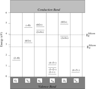
The presence of point defects in ZrSiO4 thin films will affect the performance of this material as an alternative gate dielectric in microelectronics. Recent ab initio calculationsPuthenkovilakam et al. (2004) showed that zircon forms an excellent interface with silicon providing adequate barriers for both electrons and holes (the band alignment is symmetric, with valence band offset of 2.78 eV and conduction band offset of 2.10 eV). The alignment of the defect levels with the valence and conduction band edges will determine whether these defects can play a role in the conductivity properties of the barrier. Figure 4 show the calculated defect transition energy levels with the reference of the calculated silicon valence and conduction band edges presented in Ref. [Puthenkovilakam et al., 2004]. The defect levels are relatively deep. The acceptor levels for Oi, V, and V can trap electrons injected from the top of the silicon valence band. The donor level for oxygen vacancy lies in the silicon energy gap and can act as hole-killer center for p-type doped silicon, or trap electrons for n-type doped silicon. The level for Zr interstitial practically resonates with the bottom of the silicon conduction band, and would act as a shallow donor. Donor levels for interstitial Si lie just above the silicon conduction band minimum and would readily produce electrons into the device.
| Defect | ||||
|---|---|---|---|---|
| high-C | low-C | high-C | low-C | |
| O | ||||
| O | ||||
| Oi | ||||
| O | ||||
| V | ||||
| VO | ||||
| V | ||||
| V | ||||
| Sii | ||||
| Si | ||||
| Si | ||||
| Si | ||||
| Si | ||||
| V | ||||
| V | ||||
| V | ||||
| V | ||||
| VSi | ||||
| Zri | ||||
| Zr | ||||
| Zr | ||||
| Zr | ||||
| Zr | ||||
| V | ||||
| V | ||||
| V | ||||
| V | ||||
| VZr | ||||
| ZrSi | ||||
IV Conclusions
We have used first principles simulations to study the energetics of high and low concentrations of point defects in zircon. The effect of volume swelling induced by high concentration of defects in the formation energies is of the order of tenths of eV, and is not affecting the relative stability of the intrinsic point defects. We have seen that interstitials and vacancies of oxygen and the Zr and Si anti-sites are the most stable defects. There is a strong tendency towards ionization of the defects, and a negative-U behaviour was observed for some defects in this material. Interstitials of oxygen, and the vacancies of Zr and Si may act as traps for electrons, while vacancies of oxygen and cation interstitials would serve as traps for holes. The strong ionic character of cation defects is also shown by the charge transfer between vacancies and interstitials to form neutral Frenkel pairs. The deep defect levels induced in the gap will increase the leakage and reduce the performance of zircon as a gate dielectric. The presence of high concentration of charged defects in zircon for nuclear waste immobilization will create internal electric fields that can affect the kinetics of impurity mobility and their effect has to be included in any modelization of these materials.
Acknowledgements.
This work was supported by British Nuclear Fuels (BNFL) and NERC. We would like to thank E. K. H. Salje, M. T. Dove, K. Trachenko, M. Yang, S. Rios, I. Farnan for helpful discussions on zircon.References
- et. al. (1998) W. J. W. et. al., J. Mater. Res. 13, 1434 (1998).
- Ewing et al. (1995) R. C. Ewing, W. Lutze, and W. J. Weber, J. Mater. Res. 10, 243 (1995).
- Holland and Gottfried (1955) H. D. Holland and D. Gottfried, Acta Cryst. 8, 291 (1955).
- Ríos et al. (2000) S. Ríos, T. Malcherek, E. K. H. Salje, and C. Domeneghetti, Acta Cryst. B56, 947 (2000).
- Wilk and Wallace (2000) G. D. Wilk and R. M. Wallace, Appl. Phys. Lett. 76, 112 (2000).
- Crocombette (1999) J.-P. Crocombette, Phys. Chem. Minerals 27, 138 (1999).
- Ordejón et al. (1996) P. Ordejón, E. Artacho, and J. M. Soler, Phys. Rev. B 53, 10441 (1996).
- Soler et al. (2002) J. M. Soler, E. Artacho, J. D. Gale, A. García, J. Junquera, P. Ordejón, and D. Sánchez-Portal, J. Phys.: Condens. Matter 14, 2745 (2002).
- Hohenberg and Kohn (1964) P. Hohenberg and W. Kohn, Phys. Rev. 136, B864 (1964).
- Kohn and Sham (1965) W. Kohn and L. J. Sham, Phys. Rev. 140, A1133 (1965).
- Ceperley and Alder (1980) D. M. Ceperley and B. J. Alder, Phys. Rev. Lett. 45, 566 (1980).
- Troullier and Martins (1991) N. Troullier and J. L. Martins, Phys. Rev. B 43, 1993 (1991).
- Kleinman and Bylander (1982) L. Kleinman and D. Bylander, Phys. Rev. Lett. 48, 1425 (1982).
- Junquera et al. (2001) J. Junquera, O. Paz, D. Sánchez-Portal, and E. Artacho, Phys. Rev. B 64, 235111 (2001).
- Pruneda et al. (2004) J. M. Pruneda, T. D. Archer, and E. Artacho, Phys. Rev. B 70, 104111 (2004).
- Rignanese et al. (2001) G. M. Rignanese, X. Gonze, and A. Pasquarello, Phys. Rev. B 63, 104305 (2001).
- Robinson et al. (1971) K. Robinson, G. V. Gibbs, and P. H. Ribbe, Am. Mineral. 56, 782 (1971).
- Makov and Payne (1995) G. Makov and M. C. Payne, Phys. Rev. B 51, 4014 (1995).
- Laks et al. (1992) D. B. Laks, C. G. V. de Walle, G. F. Neumark, P. E. Blöchl, and S. T. Pantelides, Phys. Rev. B 45, 10965 (1992).
- Fiorentini and Gulleri (2002) V. Fiorentini and G. Gulleri, Physical Review Letters 89, 266101 (pages 4) (2002), URL http://link.aps.org/abstract/PRL/v89/e266101.
- Jr. (1998) M. W. C. Jr., NIST-JANAF thermochemical tables (1998).
- Pantelides et al. (1974) S. T. Pantelides, D. J. Mickish, and A. B. Kunz, Phys. Rev. B 10, 5203 (1974).
- Robertson (2000) J. Robertson, J. Vac. Sci. Technol. B 18, 1785 (2000).
- Foster et al. (2002) A. S. Foster, F. L. Gejo, A. L. Shluger, and R. M. Nieminen, Phys. Rev. B 65, 174117 (2002).
- Zhang et al. (2001) S. B. Zhang, S.-H. Wei, and A. Zunger, Phys. Rev. B 63, 075205 (2001).
- Trachenko et al. (2002) K. Trachenko, M. T. Dove, and E. K. H. Salje, Phys. Rev. B 65, 180102 (2002).
- Farnan and Salje (2001) I. Farnan and E. K. H. Salje, J. Appl. Phys. 89, 2084 (2001).
- Anderson (1975) P. W. Anderson, Phys. Rev. Lett. 34, 953 (1975).
- Foster et al. (2001) A. S. Foster, V. B. Sulimov, F. L. Gejo, A. L. Shluger, and R. M. Nieminen, Phys. Rev. B 64, 224108 (2001).
- Puthenkovilakam et al. (2004) R. Puthenkovilakam, E. A. Carter, and J. P. Chang, Phys. Rev. B 69, 155329 (2004).