Holes in the valence band of superconducting boron-doped diamond film
studied by soft X-ray absorption and emission spectroscopy
Abstract
Carbon- and boron-2 states of superconducting and non-superconducting boron-doped diamond samples are measured using soft X-ray emission and absorption spectroscopy. For the superconducting sample, a large density of hole states is observed in the valence band in addition to the states in the impurity band. The hole states in the valence band is located at about 1.3 eV below the valence band maximum regardless of the doping level, which cannot be interpreted within a simple rigid band model. Present experimental results, combined with the first principles calculations, suggest that superconductivity is to be attributed to the holes in the valence band.
pacs:
81.05.Uw, 71.55.-i, 74.25.Jb, 78.70.En, 78.70.DmRecent discovery of superconductivity in heavily boron-doped diamondekimov has brought up renewed interest in the physics of doped insulating/semiconducting systems. Diamond has always been a very attractive material because of its characteristic physical properties, and boron has been well known as an impurity in diamond along with nitrogen and phosphorus, which makes an acceptor level at 0.37 eV above the top of the valence band.thonke Heavily boron-doped diamond has been known to be metallic since the late ’90s (the concentration for insulator-metal transition = 21020 cm-3), but due to the large band gap ( 5.5 eV) the possibility of superconductivity in diamond had not been noticed for some time, despite the fact that graphite-related compounds and diborides have been studied extensively.nagamatsu
Since the discovery of superconductivity in boron-doped diamond, several theoretical proposals have been made. boeri ; lee ; xiang ; blase ; baskaran Theories based on conventional BCS theory are presented in an analogy with MgB2, where strong coupling of the holes at the top of the valence band to the optical phonons plays an important role.boeri ; lee ; xiang ; blase Boeriboeri and Leelee argued the superconductivity in the hole states of valence band by virtual crystal approximation, assuming that the crystal is made ”averaged carbon-bore atoms”, and pointed out the importance of the strong electron-phonon coupling. Xiangxiang and Blaseblase discussed the effect of boron impurity on the superconductivity using density functional calculations on the system including boron as impurity. Secondly, Baskaran pointed out the importance of the electron correlation in the boron-impurity band based on the resonating valence band (RVB) theory.baskaran
Now, under these circumstances, an important step towards understanding the mechanism of superconductivity is to identify the character of the carriers. Then, it is a prerequisite to perform an experimental study which determines whether the holes responsible for superconductivity reside in the impurity band or valence band. Unfortunately, there are few experimental works at present, which may be due to experimental difficulties in observing superconductivity. Recently, however, Takano et al. have successfully synthesized a superconducting diamond film using a conventional microwave plasma-assisted chemical vapor deposition (MPCVD) method.takano
Soft X-ray absorption (XAS) and emission (XES) spectroscopies near C- and B- edges are powerful tools for studying the electronic structure of the boron-doped diamond. As the dipole selection rule between the 1 core level and the 2 state governs the transition, we can obtain the partial density of states (PDOS) of carbon 2 and of boron 2 separately, which can give important information on the mechanism of superconductivity.jin_mgb2p ; jin_alb2s ; jin_mgb2s Moreover, XES spectroscopy is a bulk sensitive probe, not a surface sensitive one like photoelectron spectroscopy.
In a previous publication we paid attention to the electronic structure of the boron impurities in diamond, a non-superconducting sample, and performed XAS and XES measurements near the B- and the C- edges.jin_dia Our conclusion there is that the wave function of impurity B-2 strongly hybridizes with the host C-2 in lightly boron-doped diamond specimen.
In this Letter, we study the electronic structure of both B-2 and C-2 in the superconducting and non-superconducting diamond films using XAS and XES spectroscopy near the B- and the C- edges. The experimental results are further analyzed in detail with the aid of first-principles band calculations. For the superconducting sample, a large electronic density of hole states is observed in the valence band in addition to the states in the impurity band. The hole states in the valence band is located at about 1.3 eV below the valence band maximum, which is larger than what is expected from the band calculation results. Moreover, this energy is not sensitive to the doping level, which cannot be interpreted within a simple rigid band picture. Although the impurities do form a band, superconductivity is attributed to the holes in valence band because the Fermi level lies within this band.
Boron-doped diamond thin films were deposited on Si (001) wafers in MPCVD.takano ; kamo ; yano Three diamond samples with different boron-concentrations were used; sample labeled ”sample-S”shows superconductivity at = 3.7 K, and labeled ”sample-N1” and ”-N2” do not show above 1.75 K using SQUID measurements. The boron concentrations are estimated by SIMS measurement to be about 4.3at%B, 0.25at%B and 0.10at%B for the sample-S, -N1 and N2, respectively.
The XAS and XES measurements were performed at BL-8.0.1alsbl8 of the Advanced Light Source (ALS) in Lawrence Berkeley National Laboratory (LBNL). The energy resolutions of the incoming and outgoing X-rays were 0.2 and 0.4 eV, respectively. For the calibrations of the monochromator and spectrometer, -BN, HOPG and natural diamond were used as the standard samples.ma ; skytt ; muramatsu
As mentioned in the introductory part, the B- XAS and XES spectra represent PDOS of empty and occupied B-2 states of the impurity boron, respectively. Figure 1 shows B- XAS and XES spectra of sample-S and -N1.
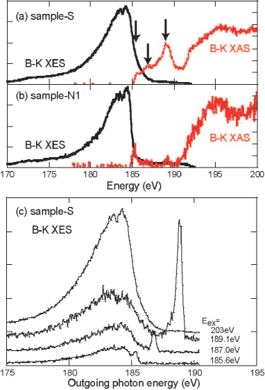
In this figure [Fig. 1 (a) and (b)], the excitation energy of the XES spectra was 200 eV in both cases. One can see the good agreement between the XES spectra of the two samples, but in the XAS spectra there is a remarkable difference in the host-gap region, 185 190 eV. The B- XAS of sample-S shows in-gap states, i.e., a broad state which fills the whole band gap region and a sharp peak at about 189 eV. These in-gap states may be attributed to boron at interstitial sites and/or boron forming clusters. The B- XAS of sample-N1 is essentially the same as our previous result of a non-superconducting samplejin_dia except a small trace of the peak at 189 eV. The Fermi level is estimated to be located at about 185.1 eV in both samples, which is a little bit lower than observed in the previous report, 185.3 eV. We attribute the difference to experimental error.
Figure 1(c) shows the B- XES with several excitation energies of sample-S, where three of them have the excitation energy of the in-gap states and one of them is a normal XES spectra with high energy excitation (= 203 eV). For all the XES spectra of sample-S, the overall features are almost the same with each other and also the same with the XES of sample-N1, which is consistent with the previous report.jin_dia
Figure 2 shows the C- XAS spectra of these samples.
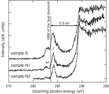
There is no incident angle dependence in the XAS and XES (following) spectra, which suggests that there is no effect of preferred orientation of nano-size crystals. The XAS spectra of sample-N1 and -N2 are almost identical, showing the impurity in-gap state labeled at 284.1 eV. However, except a small state () at 282.5 eV. In the superconductor, sample-S, this state density () increases considerably. This state is located at about 1.3 eV below the valence band maximum (VBM) of the non-doped diamond at 283.8 eV, which is shown by a dotted line.jin_dia Therefore, in the diamond superconductor, there is a considerable amount of holes in the C-2 valence band.
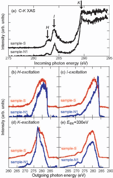
In order to gain more insight into the electronic states involved with the hole states, we performed XES measurements with an excitation energy of 282.6 eV (corresponding to state- in Fig. 2), 284.1 eV (corresponding to ), and the energy corresponding to the bottom of the conduction band (). Figure 3 shows the C- XES spectra of sample-S and -N1, where -, - and K-excitation denotes the corresponding excitation energy. At the excitation energy near the Fermi level, namely the H-excitation [Fig. 3(b)], the XES spectra of both sample-S and -N1 are the same and similar to the XES of the host diamond. This suggests that state- in the XAS spectra [Fig. 3(a)] is a state of bulk diamond, not a state of precipitation. In the I-excitation XES [Fig. 3(c)], one can see the difference between sample-S and -N1, i.e., the XES of sample-S is similar to the one with H-excitation, while that of sample-N1 displays a sharp elastic peak and a large tail on the lower energy side. The appearance of the sharp elastic peak and the large tail agrees with our previous results of non-superconductors. Since sample-S and sample-N1 differs in the density of impurities, the fact that the I-excitation XES spectra differs between the two samples suggest that state- is essentially an impurity state. In the case of K-excitation, a small difference is observed between the two samples. The spectrum of sample-N1 shows a sharp peak at 277.4 eV, which corresponds to doubly degenerated states of the C-2 valence band at point because the bottom of the conduction band (C.B.) is at point in diamond.ma2 This sharp peak broadens in sample-S, and moreover, the sharp XAS-edge at 289.6 eV (the bottom of C.B.) broadens in sample-S (Fig. 2). This may be because the symmetry of the system becomes lower due to atom substitution and/or possible lattice distortion upon boron doping. The normal XES spectra are in good agreement with each other, and with XES of the host-diamond.
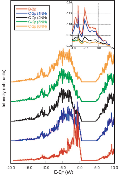
In order to analyze the experimental spectra, we performed first-principles band-structure calculations for a diamond with substitutional single B impurity using two kinds of super-cell [nominally C31B1 (3.1at%B) and C63B1 (1.6at%B)]. Figure 4 shows the calculated 2 PDOS using the C63B1 super-cell. 1NN, 2NN, 3NN and 6NN C indicate 1st, 2nd, 3rd and 6th nearest neighbor carbon from the impurity boron atom, respectively. The density of states of the first nearest neighbor carbon (1NN C) is large at around the Fermi energy and has hole states above the Fermi energy. This feature is consistent with the result obtained by DV-X method in our previous study.jin_dia In contrast with this, the density of states of 6NN C, which is far from the impurity boron, is similar to the PDOS of the non-doped diamond (bulk), but shows a small number of holes around the Fermi level (see the inset of Fig. 4). For the C31B1 super-cell, heavy-doped case, the density of states of 4th neighbor carbon (4NN C, not shown) which is farthest from the impurity boron in this cell has a notable number of holes above the Fermi energy, i.e., the hole state around the Fermi level increases with an increase of boron concentration.
Now let us go back to the data for the C- edge with these band calculation results in mind. The XES result at energy- excitation of sample-N1 [Fig. 3(b)] is very similar to the PDOS of first nearest neighbor carbons (Fig. 4). Therefore, the impurity states can be interpreted to be of localized one in the non-superconducting sample. However, for sample-S, the XES at energy- excitation is very similar to the PDOS of the bulk diamond. This means the carbons involving the impurity hole states are of bulk carbons, i.e. the impurity states make a band. Thus, we may conclude that the impurity state of sample-N1 is localized while the impurity state of sample-S forms a band.
The XES results at excitation energy- of sample-S and -N1, shown in Fig. 3(b), are very similar to the PDOS of bulk carbons rather than that of first nearest neighbor carbon. As energy is located at about 1.3 eV below VBM, we attribute the hole states at energy to the hole states in the valence band. Since this valence band hole state lies right next to the Fermi level, we may conclude that the holes in the valence band plays an essential role in the occurrence of superconductivity.
If we look more quantitatively into the energy of the peak , its location seems to be somewhat lower than what is expected from the first-principles calculation. Namely, the Fermi energy obtained from our band calculation is 0.7 eV and 0.5 eV below the VBM for 32-atom and 64-atom super-cells, respectively, which is smaller than 1.3 eV. More interestingly, the energy of peak does not depend on the doping level, and only its XAS intensity grows with doping (see Fig. 2), which cannot be understood within a simple rigid band picture. This curious doping dependence of peak remains as an interesting future problem.
In conclusion, the partial density of states of the C-2 state and the B-2 states of superconducting and non-superconducting boron-doped diamond samples have been measured using soft X-ray emission and absorption spectroscopy on C- and B- edges. For the superconducting sample, a large electronic density of states of holes has been observed in the valence band in addition to the states in impurity band. However, the hole states in valence band located at around 1.3 eV below the valence band maximum cannot be interpreted within a simple rigid band model. Although our results show that the impurity states do form a band in the superconducting sample, the holes in the valence band seems to be more important for superconductivity because the Fermi level lies within the valence band.
We express our thanks to Prof. M. Tachiki of National Institute for Materials Science (NIMS) and Prof. A. Natori of University of Electro-Communications for useful discussions. This work was performed under the approval of ALS-LBNL, proposal No. ALS-00931. ALS is supported by the Director, Office of Science, Office of Basic Energy Sciences, Materials Sciences Division, of the U.S. Department of Energy under Contract No. DE-AC03-76SF00098 at LBNL.
References
- (1) E.A. Ekimov et al., Nature, 428, 542(2004).
- (2) K. Thonke, Semicond. Sci. Tech. 18, S20 (2003), and refs. therein.
- (3) J. Nagamatsu et al., Nature (London) 410, 63 (2001).
- (4) L. Boeri et al., cond-mat/0404447.
- (5) K.W. Lee et al., cond-mat/0404547.
- (6) H.J. Xiang et al., cond-mat/0406446.
- (7) X. Blase et al., cond-mat/0407604.
- (8) G. Baskaran, cond-mat/0404286.
- (9) Y. Takano et al., cond-mat/0406053., Appl. Phys. Lett. 85, (2004) (in press).
- (10) J. Nakamura et al., Phys. Rev. B 64, 174504 (2001).
- (11) J. Nakamura et al., J. Phys. Soc. Jpn. 71, 408 (2002).
- (12) J. Nakamura et al., Phys. Rev. B 68, 064515 (2003).
- (13) J. Nakamura et al., cond-mat/0407438, accepted to Phys. Rev. B.
- (14) M. Kamo et al., J. Cryst. Growth 62, 642 (1983).
- (15) T. Yano et al., J. Electrochem. Soc. 145, 1870(1998).
- (16) J.J. Jia et al., Rev. Sci. Instrum. 67, 3372(1996).
- (17) Y. Ma et al., Phys. Rev. Lett. 71, 3725(1993).
- (18) P. Skytt et al., Phys. Rev. B50, 10457(1994)
- (19) Y. Muramatsu et al., Spectrocimica Acta A59, 1951(2003).
- (20) Y. Ma et al., Phys. Rev. Lett. 69, 2598(1992).
- (21) J.W. Ager III et al., Appl. Phys. Lett. 66, 616(1995).
- (22) R. J. Zhang et al., Diamond Rel. Mat. 5, 1288(1996).