Observation of the Fano-Kondo Anti-Resonance
in a Quantum Wire
with a Side-Coupled Quantum Dot
Abstract
We have observed the Fano-Kondo anti-resonance in a quantum wire with a side-coupled quantum dot. In a weak coupling regime, dips due to the Fano effect appeared. As the coupling strength increased, conductance in the regions between the dips decreased alternately. From the temperature dependence and the response to the magnetic field, we conclude that the conductance reduction is due to the Fano-Kondo anti-resonance. At a Kondo valley with the Fano parameter , the phase shift is locked to against the gate voltage when the system is close to the unitary limit in agreement with theoretical predictions by Gerland et al. [Phys. Rev. Lett. 84, 3710 (2000)].
pacs:
72.15.Qm, 73.21.La, 73.23.HkThe experimental realization of the Kondo effect Kondo in a semiconductor quantum dot (QD) has opened up a new human-made stage to investigate many body effects gordon . In a previous paper, we have shown that spin-scattering at a QD, which means the creation of a spin-entangled state between a localized spin and a conduction electron, leads to quantum decoherence Aikawa ; Koenig . At the same time, however, such an entangled state is a starting point to build a Kondo singlet Yosida , in which the coherence of electrons is expected to be recovered.
The direct evidence for the coherence of the Kondo state is the interference effect through a QD in the Kondo state. Ji et al. measured the phase shift of electrons through a dot in the Kondo state in an Aharonov-Bohm (AB) ring Ji , and found that the phase shift significantly varies even on the Kondo plateau of conductance, which may suggest the breakdown of the Anderson model. However, the difficulty in measuring the phase shift in AB geometry is pointed out Aharony , and experiments in simpler structures such as a stub-resonator (a schematic diagram is shown in Fig. 1(a)) Kang ; Thimm are desired.
Some of the present authors have reported the observation of the Fano anti-resonance in a quantum wire with a side-coupled QD Kobayashi_antifano , which is a kind of a stub-resonator. The Fano effect Fano is a consequence of interference between a localized state and a continuum, which correspond to a state in the QD and that in the wire, respectively. It appears as a characteristic line shape in the conductance as
| (1) |
where is the energy difference from the resonance position normalized with the width of the resonance, and is Fano’s asymmetric parameter Kobayashi . The Fano parameter represents the degree of distortion and corresponds to an anti-resonance dip. The Fano-Kondo effect – the Fano effect which appears in the Kondo cloud – is hence sensitive to coherence and phase shifts Hofstetter . In this Letter, we report the observation of the Fano-Kondo anti-resonance in a quantum wire with a side-coupled QD. Phase shift locking to is deduced from the analysis of the line shape of the anti-resonance.
Our device consists of a quantum dot and a quantum wire difined in a two-dimensional electron gas (2DEG, sheet carrier density , mobility ) formed at a GaAs/AlGaAs hetero-structure. Au/Ti metallic gates were deposited as shown in Fig. 1(b). A QD is defined by the upper three gates and the two gates marked as “M” (M-gates). The lower three gates adjust the conductance of the wire. The middle of the upper gates is used to control the potential of the dot (gate voltage ) and M-gates tune the coupling between the dot and the wire (gate voltage ). It was confirmed that the system works as a quantum wire with no quantum dot when M-gates are pinched-off. Tuning the coupling strength by M-gates induces the electrostatic potential shift of the dot, whereas the potential shift by causes little change in the coupling strength. Accordingly, the potential shift by can be compensated by (approximately in the present sample). For the sake of a simpler description, we henceforth redefine . In order to attain a large value of Kondo temperature , the device was designed to make the dot size smaller than that used in Ref. Kobayashi_antifano . The dot is placed close to the wire to avoid temperature dependence associated with a change of the coherence length, which is unfavorable for the present study. Although the proximity of the dot to the wire would cause a Fano-charging mixing effect Johnson , it is less severe in a comparatively strong coupling regime explored here. The sample was cooled in a dilution refrigerator down to 30 mK and was measured by standard lock-in techniques in a two-terminal setup.
In order to obtain the relevant parameters of the dot, we first measured the direct charge transport through the dot (from “Source1” to “Drain” in Fig. 1(b)) by slightly opening and by closing and . The average level spacing obtained from excitation spectroscopy is about 0.3 meV, which gives the dot diameter as about 170 nm and the total number of electrons as about 90. The electron temperature estimated from the widths of resonance peaks followed the fridge temperature down to 100 mK and severe saturation occurred below that. Then the direct connection was pinched off by and the wire was opened by . The wire conductance far from (anti-)resonances was adjusted to be around , i.e., at the first step of the conductance staircase.
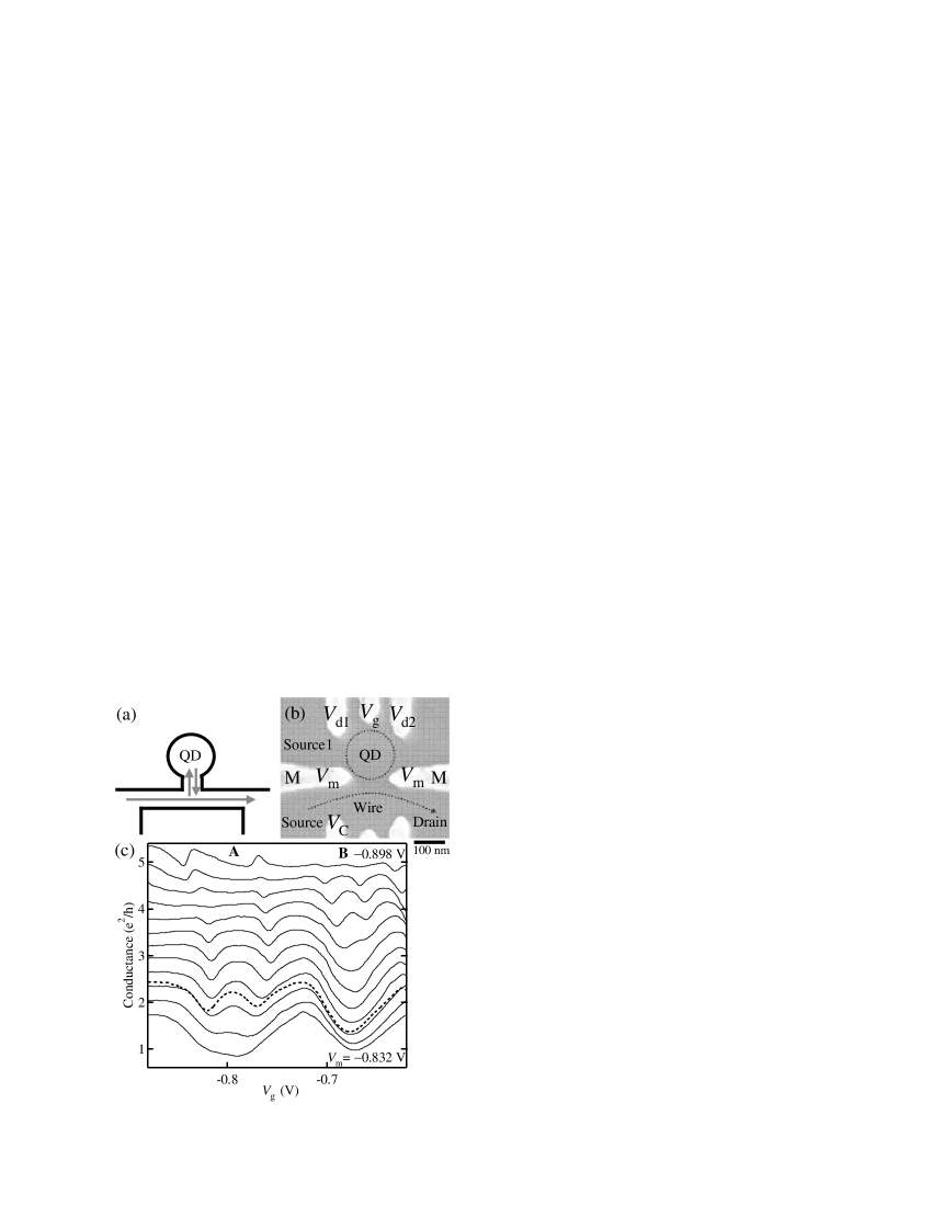
Figure 1(c) shows the wire conductance against at various coupling strength adjusted by . In a weak coupling regime (at the top of Fig. 1(c)), Coulomb “dips” appear, reproducing the previous result Kobayashi_antifano . This is due to the destructive interference, i.e., the Fano anti-resonance. These dips are regularly placed and the averaged period is the same as that of the Coulomb oscillation in the direct transport. This indicates that the dips are originated from the QD. As the coupling strength increases, conductance between the dips (Coulomb valleys) decreases alternately. These reductions connect two neighboring dips into one (in regions A and B). We have observed four such valleys (as will be shown in Fig. 2) where the conductance decreases as the coupling strength increases. We next confirm that these reductions are due to the Fano-Kondo anti-resonance, then discuss the obtained information.

The upper panel of Fig. 2 shows the zero-bias wire conductance as a function of at three different temperatures for a medium coupling strength. The closed bars indicate the positions of the Coulomb dips. For valley B, the positions cannot be resolved directly and are extrapolated from the positions at V. In the four regions indicated as A-D, conductance decreases with decreasing temperature. The Kondo effect for spin 1/2 emerges for a QD with odd number of electrons. Hence it usually appears alternately at Coulomb valleys as we observed at Kondo valleys A-D.
The distances between the Coulomb dips are shorter at the Kondo valleys than those at the neighboring valleys. The level spacing obtained from this difference of the distances is in good agreement with obtained from excitation spectroscopy. This means the simple “spin-pair” picture is holded and the conditions for the Kondo effect are fulfilled at valleys A-D.
The lower panel of Fig. 2 is a color scale plot of the conductance on the plane of and the source-drain bias voltage . The conductance drops around mV at the Kondo valleys. Note that is not directly applied to the dot but to the wire. The wire by itself can show non-linear conductance Kristensen . In this experiment, however, the non-linearity of the wire is small, because the wire is under the plateau condition and the scale of is magnitude smaller than that in the previous reports Kristensen . Furthermore, the response to and the reversed Coulomb diamond like structure (not well resolved in Fig. 2) indicate that the zero-bias “dips” originate from the Kondo effect of the dot. The charging energy estimated from the reversed Coulomb diamond ranges from 0.3 to 0.5 meV. For a quantitative comparison with existing theories, we should be careful to multi-level effect, which is usually ignored by taking the limit of infinite (or charging energy). Such “single-level” approximation is expected to hold when the separation of Coulomb peaks (dips) is clear. We therefore concentrate on dip A, which shows the clearest seperation.
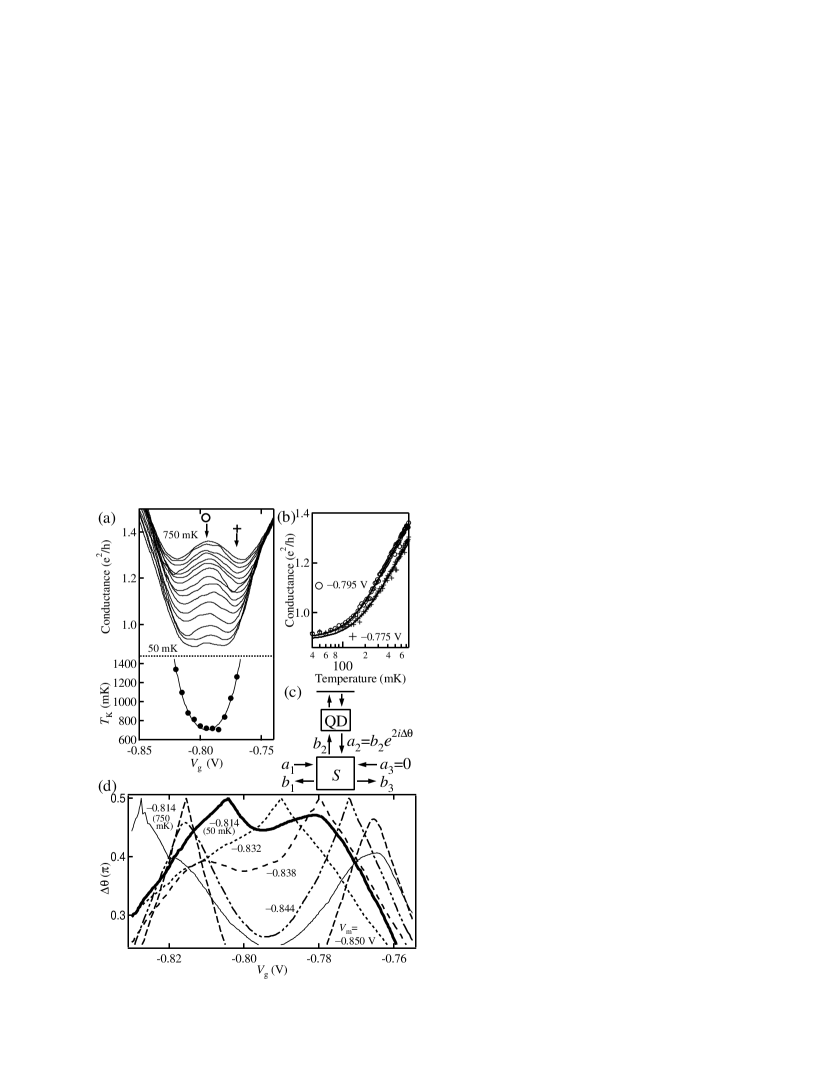
The upper panel of Fig. 3(a) shows detailed temperature dependence of at Kondo valley A. We obtained the Kondo temperature from the form costi :
| (2) |
where , , and are fitting parameters. was fixed to 1.8, the wire conductance far from the anti-resonance. Examples of the fitting are shown in Fig. 3(b). The data below 120 mK are not taken into the fitting considering the electron temperature saturation. From the fitting, was obtained, which is in accordance with the prediction for spin 1/2 impurities. The obtained are plotted against in the lower panel of Fig. 3(a). depends parabolically on with the bottom around the mid-point of the Kondo valley just like the previous reports vanderwiel . This dependence agrees well with , where is the dot-wire coupling and is the single electron level measured from the Fermi level. We obtained meV and meV by fitting the above function to .
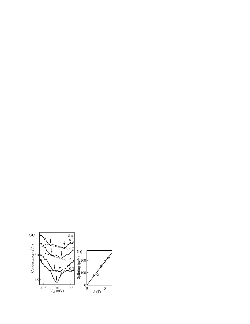
Figure 4(a) shows the splitting of the zero-bias conductance dip under the external magnetic field parallel to the 2DEG. The splitting is proportional to the field as shown in Fig. 4(b) and attributed to the Zeeman splitting of the Kondo anomaly. From the slope of the fitted line, we obtain the g-factor of electrons as , which is close to that reported for GaAs/AlGaAs 2DEG Jiang .
So far we have confirmed that the conductance reduction in regions A-D in Fig. 2 is due to the Fano-Kondo anti-resonance. In the side-coupled geometry, only destructive interference can cause the conductance reduction. The observation of the Kondo effect through the pure interference effect manifests that electron transport through the Kondo cloud is coherent as predicted Kang .
In Fig. 1(c), two dips merges into one in regions A and B. This means the system almost reaches the unitary limit vanderwiel . This is consistent with the obtained shown in the lower panel of Fig. 3. The residual conductance at the “unitary limit” Kondo valleys (e.g., 0.7 at valley B in Fig. 2) is probably due to the finite area between the wire and the dot, which works as a resonator and spoils the perfect reflection Thimm , while the phase shift is unchanged because .
When the coupling is weak (at the top of Fig. 1(c)), the two dips at both sides of valley A have asymmetric Fano line shapes (). It has been anticipated that symmetry of transport through a QD is dominated by a few states with an anomalously strong coupling to an electrode (strong coupling states, SCSs) Silvestrov . In a weak coupling regime, the ’s of the two dips at both sides of valley A are hence determined by an SCS. As the coupling strength increases, however, the values of approach to zero indicating that the coupling strength is renormalized and the Kondo state takes over the SCS.
We now discuss the phase shift of Kondo state, which can be obtained from the analysis along the scattering form of conductance. A simple model of the system : a three branch S-matrix and a reflector (the QD), is shown in Fig. 3(d). Here we take the S-matrix simply as
| (3) |
Assuming the absense of reflection from the electrodes we put . And taking the QD as a transmitter plus a perfect reflector, we put and for unitary input. Then the phase shift is easily obtained as
| (4) |
Here is the complex transmittance and related with the conductance through the Landauer formula as . The specific form of (3) does not spoil the generality. The time-reversal symmetry, the unitarity and impose strong constraints on the S-matrix and the residual freedom has very little effect.
Figure 3(d) shows thus calculated . Here we take plus of the double sign in (4), which causes the virtual folding at . This is due to the special condition of and the folding does not disturb the confirmation of locking to . As temperature decreases from 750 mK to 50 mK and the coupling becomes stronger from V to V, the phase shift variation approaches to the stationary line of at the Kondo valley. This is in accordance with the existing theories gerland and in contrast to the previous result Ji , where only locking to at pre-Kondo region was observed. The difference may come from the width of the energy levels gerland , or from the geometry of the interferometer, though we have no conclusive opinion at present.
In Fig. 2, zero-bias anomalies appear while no voltage was directly applied to the dot. This indicates that the Kondo cloud spreads into the wire and is affected by . This is reasonable considering the size of the Kondo cloud (: Fermi velocity), which exceeds 2 m for less than 1 K Simon . The present structure provides means to investigate the size of the Kondo cloud.
In summary, we have observed the Fano-Kondo anti-resonance in a quantum wire with a side-coupled dot. Phase shift locking to is deduced from the line shape of the anti-resonance.
This work is supported by a Grant-in-Aid for Scientific Research and by a Grant-in-Aid for COE Research from the Ministry of Education, Culture, Sports, Science, and Technology of Japan.
References
- (1) J. Kondo, in Solid State Physics Vol. 23, p. 13 (Academic Press, New York, 1969).
- (2) D. Goldhaber-Gordon et al., Nature 391, 156 (1998); S. M. Cronenwett et al., Science 281, 540 (1998); J. Schmid et al., Physica (Amsterdam) 256B-258B, 182 (1998).
- (3) H. Aikawa et al., Phys. Rev. Lett. 92, 176802 (2004).
- (4) J. König and Y. Gefen, Phys. Rev. Lett. 86, 3855 (2001); Phys. Rev. B 65, 045316 (2002).
- (5) K. Yosida and A. Yoshimori, Magnetism V, edited by H. Suhl (Academic Press, 1973).
- (6) Y. Ji et al., Science 290, 779 (2000); Y. Ji, M. Heiblum, and H. Shtrikman, Phys. Rev. Lett. 88, 076601 (2002).
- (7) A. Aharony et al., Phys. Rev. B 66, 115311 (2002).
- (8) K. Kang et al., Phys. Rev. B 63, 113304 (2001); A. A. Aligia and C. R. Proetto, Phys. Rev. B 65, 165305 (2002); M. E. Torio, et al., Phys. Rev. B 65, 085302 (2002).
- (9) W. B. Thimm, J. Kroha, and J. von Delft, Phys. Rev. Lett. 82, 2143 (1999).
- (10) K. Kobayashi et al., Phys. Rev. B 70, 035319 (2004).
- (11) U. Fano, Phys. Rev. 124, 1866 (1961).
- (12) K. Kobayashi et al., Phys. Rev. Lett. 88, 256806 (2002); Phys. Rev. B 68, 235304 (2003).
- (13) W. Hofstetter, J. König, and H. Schöller, Phys. Rev. Lett. 87, 156803 (2001).
- (14) A. C. Johnson et al., Phys. Rev. Lett. 93, 106803 (2004).
- (15) A. Kristensen et al., Phys. Rev. B 62, 10950 (2000).
- (16) T. A. Costi, A. C. Hewson, and V. Zlatic, J. Phys. Condens. Matter 6, 2519 (1994); D. Goldhaber-Gordon et al., Phys. Rev. Lett. 81, 5225 (1998).
- (17) W. G. van der Wiel et al., Science 289, 2105 (2000).
- (18) H. W. Jiang and E. Yablonovitch, Phys. Rev. B 64, 041307(R) (2001).
- (19) T. Nakanishi, K. Terakura, and T. Ando, Phys. Rev. B 69, 115307 (2004).
- (20) U. Gerland et al., Phys. Rev. Lett. 84, 3710 (2000).
- (21) P. Simon and I. Affleck, Phys. Rev. B 68, 115304 (2003).