Electrical transport properties of stable single-atom contacts of zinc
Abstract
We report low-temperature measurements of the electrical transport properties of few-atom contacts of the superconducting metal zinc, arranged with lithographically fabricated mechanically controllable breakjunctions (MCB). The conductance histogram shows several narrow peaks, not regularly observed for multivalent metals. The first peak - corresponding to the single-atom contact - is located slightly below one conductance quantum and is split into two subpeaks, possibly indicating two preferred configurations of the single-atom contact. The current-voltage characteristics in the superconducting state show nonlinearities due to multiple Andreev reflections (MAR). In addition we find nonlinearities in the current-voltage characteristics that we attribute to electronic-interaction effects due to the granular structure of the film. Some of these latter findings are in qualitative agreement with a prediction by Avishai et al. avishai .
pacs:
PACS numbers: 73.40.Jn, 74.50.+r, 73.20.DxFor revealing and understanding the electronic transport properties of atomic scale circuits, single- or few-atom contacts are used as model systems. In this limit the electronic conduction can be regarded as a fully quantum-mechanical scattering and wave-matching problem, i.e. the conductance can be attributed to independent electronic modes, nick-named ”conduction channels”. An atomic-size contact between two metallic electrodes can accommodate only a small number of conduction channels. The transport properties are thus fully described by a set of transmission coefficients which depends both on the chemical properties of the atoms forming the contact and on their geometrical arrangement. Experimentally, contacts consisting of even a single atom have been obtained using both scanning-tunnel microscopy and breakjunction techniques agrait03 . The total transmission = of a contact is deduced from its conductance measured in the normal state, using the Landauer formula where is the conductance quantum landauer70 .
Experiments on a large ensemble of metallic contacts have demonstrated the statistical tendency of atomic-size contacts to adopt element-specific preferred values of conductance. The actual preferred values depend not only on the metal under investigation but also on the experimental conditions. However, for many metals, and in particular ’simple’ ones (like Na, Au…) which in bulk form good ’free electron’ metals, the smallest contacts have a conductance close to (Ref. agrait03 ). Statistical examinations of Al point contacts at low temperatures yield preferred values of conductance at and (Ref. yansoncomment ), indicating that single-atom contacts of Al have a typical conductance slightly below the conductance quantum.
However, it has been shown by the analysis of current-voltage (IV) characteristics in the superconducting state that Al single-atom contacts accommodate in general three transport channels, the transmissions of which add up to a value around 1 (Ref. aluprl ). These findings are in agreement with measurements of the shot noise brom ; cron , conductance fluctuations ludoph1 , thermopower ludoph2 and the supercurrent goffman in such contacts. A quantum chemical model nature which links the to the chemical valence and the atomic arrangement of the region around the central atom of the constriction, has been put forward. This model predicts that monovalent metals would transmit a single channel while sp-like metals as e.g. Al or Pb up to four channels due to the contributions of the (unoccupied) p orbitals. So far Al appears to be the only metal with the property to show peaks in the histogram close to multiples of although this does not correspond to quantized transmission values.
According to simplistic arguments and ignoring the band structure, divalent elements such as the alkaline-earth elements or the IIB subgroup elements Cd, Zn and Hg, should be insulating, since they have a completely filled outer s-shell. This apparent discrepancy to the experimental findings indicates that additional orbitals besides the s-orbitals contribute to the electronic conductance. Tight-binding calculations reveal that in the case of Zn the 4p orbitals are the most relevant ones for a correct description of the bulk band structure (Ref. papaconstantopoulos ). With these considerations, single-atom contacts of Zn are expected to have very similar transport properties as Al single-atom contacts, i.e. up to four channels with a total conductance of about 1 nature . The distribution of the transmission coefficients, however, may deviate, since it depends on the exact atomic configuration. Since Zn crystallizes in a hexagonal, slightly distorted hcp structure while Al is a fcc crystal, the actual atomic arrangement of the point contacts might be different. Moreover, due to the ”loss” of many neighbors, a single Zn atom in a contact may behave more atomic-like.
Here, we report the fabrication and low-temperature electronic transport properties of lithographic MCBs of Zn. This work represents the first study of atomic-size contacts of Zn. The measurements in the normal state demonstrates the tendency of the atomic-size contacts to adopt preferred conductance values. The analysis of the current-voltage characteristics reveals superconducting properties of the nanowires as well as indications of electron-electron interactions. We show data of four, nominally identical samples, labeled No. 1 to 4.
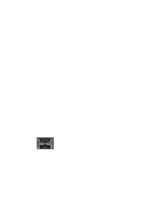
The samples are fabricated along the lines of Ref. jansaclay . Our samples are 2 m long, 200 nm thick suspended Zn nanobridges, with a constriction in the center (cf. Fig. 1). The thickness of the bronze substrates is mm, the distance between the counter-supports of the bending mechanism is 10 mm. With these sample parameters and the geometry of the mechanics we achieve reduction ratios (between the motion of the pushing rod and the displacement of the bridge arms) of the order of 5000:1 (see below).
Special care has to be given to the evaporation of Zn. Because of its low boiling temperature and high vapor pressure, Zn desorbs easily from the substrate if no crystallization seeds are provided. If Zn is evaporated at room temperature, it grows in islands of micron-size with the hexagonal axis preferably perpendicular to the substrate plane. Since this structure is not suitable for the formation of atomic-size contacts, we take special care to reduce the grain size. We first deposit a 1 nm thick seed layer of Ge onto the substrate which is cooled by liquid nitrogen to a temperature of . At lower substrate temperatures the different thermal expansions of the metallic substrate, the Zn itself, the polyimide sacrificial layer and the polymer lithographic mask provoke cracks in either the mask or the Zn layer on warming up to room temperature. The metal is then evaporated from a home-made boron-nitride crucible heated by a tungsten foil at a pressure of mbar and a rate of nm/s at the same substrate temperature. The parameters are chosen empirically such that the grain size of the Zn layer does not exceed nm and the adhesion is good enough for the subsequent lift-off process. Finally, the bridge is underetched in an isotropic oxygen plasma which reduces the height of the polyimide layer by about 300 to 500 nm. At the narrow constriction the nanobridge is now unsupported. The resistance of the nanobridge does not increase during the etching process, indicating that reaction between the oxygen ions and Zn is weak.
The bridge is then mounted on a three point bending mechanism on a stick which is immersed into liquid helium and can be pumped down to reach temperatures of 1.5 K. The residual resistivity ratio of the bridges is typically RRR = from which we deduce an elastic mean free path of 13 nm. On an unpatterned thin film of the same thickness we measured the critical temperature K and a perpendicular critical field of mT. is slightly reduced with respect to the bulk critical temperature of K while is enhanced, as usual in thin films ( mT) (Ref. kittel ).
As a first step we have determined the preferred conductance values of few-atom contacts when opening or closing continuously and have constructed the corresponding conductance histograms.
A screw with 500 m pitch, driven by a dc-motor on top of the cryostat through an (exchangeable) reduction gear box, controls the motion of the pushing rod that bends the substrate. The relative displacement of the pushing rod can be controlled to a precision of m, which due to the geometry of the bending mechanism results in a relative motion of the two anchor points of the bridge of around 0.9 pm. This was verified using the exponential dependence of the conductance on the inter-electrode distance in the tunnel regime. The absolute precision is restricted due to hysteresis of the bending mechanism (torsion of the pushing rod etc.) and roughness of the screw pitch to about 100 nm for the pushing rod (corresponding to 0.02 nm for the bridge). We note that the stability of the setup allows us to halt at any point along the breaking or closing curves, even on the last plateau when the contact is formed by a single atom, without any observable drift of the measured conductance.
The resistance of the sample is recorded by a 4-point resistance bridge with a measuring current of 1 nA and a resolution of in a range from 200 to 200 k. Due to the mentioned texture of the evaporated film there are only few sliding planes parallel to the substrate which would allow for a stretching of the film. Consequently it often happens that the two electrodes remain separated by a gap of several nm after the first breaking. Therefore the first opening of the contact has to be performed very slowly. Typical opening speeds for the systematic measurements are 155 nm/s for the pushing rod, corresponding to a displacement of the bridge anchor points of 36 pm/s. The output of the resistance bridge is recorded by an oscilloscope and then transferred to a computer for calculating the histogram.
The conductance decreases in steps of the order of 0.2 to 1 , their exact sequence changing from opening to opening (see panel e of Fig. 2). Since the mechanical deformation is different for opening and closing, we construct separate histograms for both experiments. Fig. 2a displays the conductance histograms calculated from subsequent opening and closing sequences recorded during two weeks on sample No. 1 which has been kept at low temperatures. Similar histograms were achieved with a lower motion speed of the bridge arms of 17 pm/s. After an accidental warming up to K no step curves could be observed any more.
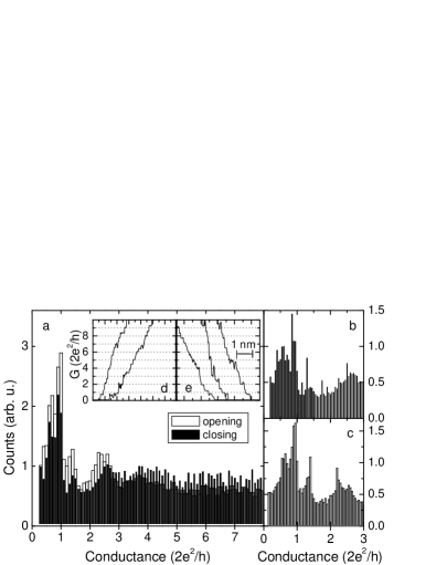
Several peaks appear for both motion directions at similar positions of , 1.4 and . Interestingly the first peak is split into two substructures at and 0.9 , a feature which has not been observed for other materials. This splitting has been observed in several independent measurements carried out with two different samples (Nos. 1 and 4). Although the splitting is observed in all our measurements, the absolute values of the peak positions and the relative peak heights vary slightly from experiment to experiment (see Fig. 2b and c). A possible explanation of the splitting would be two different configurations of the central atom e.g. different crystalline orientations or a short contact with only one plane with a single atom in cross-section vs. a dimer contact with two single atoms in series. The latter configuration has been found in molecular dynamics calculations to be typical for Au contacts just before breaking dreher . This geometrical difference gives rise to different conductances haefner . In similar experiments by Yanson et al. yansondiss on ”classical” breakjunctions made of notched Zn wires, no splitting of the first peak is found, but a shoulder that is compatible with our findings. The peaks at higher conductance values are in reasonable agreement with our findings as well. It is well known that details of the histograms do depend on the experimental conditions, as one can easily see by comparing different published results of e.g. the most extensively studied metal gold. In the experiment with Zn by Yanson et al. higher voltages have been applied, a slightly higher temperature and faster opening speeds have been used and only opening traces were recorded.
In our experiment, the main difference between opening and closing consists in the peak heights. The low-conductance peaks are less well pronounced when closing. In the closing traces (see panel d) we often observe that the first contact has a conductance well above . We attribute this to the formation of contacts larger than a single-atom contact since the apex atoms from the previous opening sequence might have relaxed back to positions deeper in the tip.
Conductance histograms of multivalent metals in general do not show well pronounced multiple peaks yansondiss ; ludoph3 ; costa-kramer . An exception of this general observation was so far Al, as mentioned already in the introduction. The histogram of Zn shows similarities to that of Al: Several peaks occur with an average spacing between the peaks of about 1.3 . One could argue whether this similarity in the preferred conductance values would be mirrored in the quantum transport properties, i.e. the conduction channels. Therefore we performed measurements in the superconducting state for the determination of the channel ensemble. For this purpose extremely stable contacts and thus a more complex bending mechanism is required. The samples are mounted onto a three-point bending mechanism thermally anchored to the mixing chamber of a dilution refrigerator and that contains now a differential screw close to the sample holder. The pushing rod of the bending mechanism is driven by a dc motor at room temperature via a mechanical feedthrough and several gear boxes with a reduction ratio of 1:2,400,000 between the turning speed of the motor and the axis entering the differential screw. The differential screw transforms one turn of the axis into a motion of the pushing rod of 100 m. The sample geometry is the same as in the previous measurements, giving again rice to a reduction ratio of 1:5000. Taking into account the reduction of the gear boxes, the differential screw and the geometry of the sample itself, one turn of the motor yields a displacement of the bridge arms of the sample of about 8 fm. Therefore, stable tunnel or few-atom wide contacts are achievable, but no histograms can be recorded within a reasonable time. For further experimental details see Refs. aluprl and physicab . Contrary to the experiments described in aluprl , only lossy coaxial wires and twisted-pair wires in capillaries were used for high-frequency filtering. This restricts the electronic temperature of the samples to about 160 mK.
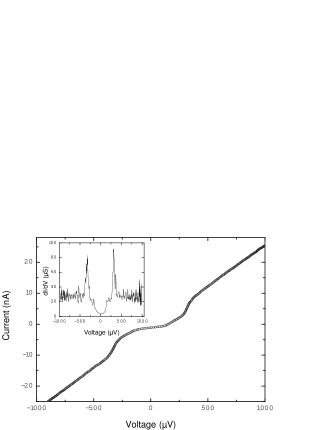
Fig. 3 depicts a current-voltage sweep (IV) measured at mK when sample No. 2 was in the close tunnel regime with a conductance of . In the inset, the differential conductance is shown. The tunnel contact was achieved by carefully closing the contact right before the so-called ”jump to contact”, i.e. the strong conductance increase signalling hte formation of an atomic bond between the two bridge arms agrait03 . Apparently, the spectrum deviates from the expected behavior for BCS superconductors, as has already been observed in earlier studies of tunnel contacts of Zn fabricated by different methods tomlinson . We deduce a superconducting gap V, somewhat higher than the values found in the literature, which vary typically between eV and eV, depending on the measuring method, crystallographic orientation and other parameters tomlinson . After these characterization measurements, we close the bridge again to form single- or few-atom contacts. This is done by reducing the bending of the substrate until the sample achieves a conductance of and opening it again carefully. Just before break typically conductances of are observed.
In Fig. 4 we depict a typical set of IVs recorded on contacts on last plateaus of sample No. 2 before breaking of the wire, measured at temperatures around 160 mK. The typical nonlinearities due to multiple Andreev reflection (MAR) are observable averin ; carlosprb . However, they appear rounded compared to the theoretical prediction and the observations for contacts of superconductors with a density of states obtained from vs. that is closer to the BCS shape. This fact limits the precision with which the channel ensemble can be determined. The lines shown in Fig. 4 are fits to the theory of MAR taking into account 1, 2 or 4 channels for curves a, b, and c (all measured on sample No. 2). Because of the rounded MAR structures, only the number of channels can be estimated, but no meaningful value for the transmissions can be given for contacts with more than one channel because several channel transmissions combinations give fits with the same quality. The fact that the determination of the number of channels is more robust than the precision with which the individual transmissions can be deduced has already been reported for few-atom contacts of Nb, a metal that also shows a DOS deviating from the BCS shape ludoph3 . The robustness of the determination of the number of channels is due to the super-linear dependence of the excess current (the extrapolated intersection of the high-bias current with the current axis) on the transmission values averin ; carlosprb . Interestingly, contacts with a dominating single channel, accompanied by a second, but much smaller one, similar to the observations for Au agrait03 ; scheer01 , are achievable. These IVs are routinely observed at the end of a last plateau after an abrupt change of the IV including an increase of the conductance, and thus an re-arrangement of the atomic-size contact. Once such a contact has been established, it remains stable for an elongation of the bridge of 1-2 Å. For Al samples, contacts with a dominating channel with the contribution of one or two smaller channels could be observed as well aluprl ; goffman . However, for Al these contacts evolved continuously from a situation with three channels of similar size and occurred only very rarely boehler .
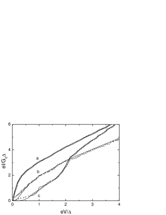
The origin of these single-channel like contacts and their possible correlation with the observed splitting of the first maximum in the conductance histogram has to be clarified further. Therefore, measurements on contacts, fabricated from whisker breakjunctions have been carried out. The results of these investigations together with a detailed theoretical analysis will be reported elsewhere haefner . We expect the superconducting DOS to be closer to the BCS DOS for those samples and consequently allowing to determine the transmission values precisely.
Another observation hampers the quantitative determination of . As can be seen in curve c of Fig. 4, the current onsets corresponding to MAR processes involving two or more electrons seem to be shifted to higher voltages with respect to the current onsets predicted by the theory and observed for contacts of other superconductors nature . We attribute this observation to the onset of Coulomb blockade grabert due to the granularity of the film. Our findings are in qualitative agreement with a prediction by Avishai et al. avishai . The authors have calculated the IV characteristics of an interacting quantum dot between two superconductors and found a decrease of the subgap current and a shift of the higher-order MAR processes to higher voltages. However, since no quantitative theory for our experimental realization and resulting transmission coefficients are available, we cannot perform a quantitative comparison with this suggestion.
Cron et al. crondiss have placed an Al breakjunction in a high-impedance environment in order to study the dynamic Coulomb blockade grabert of a single junction. They found a reduction of the low-bias conductance in reasonable agreement with a theoretical model when the contact was driven normalconducting by applying a small magnetic field. However, no effect was detected in the superconducting state.
In order to test the interpretation of Coulomb blockade, we record IVs of tunnel contacts for various magnetic fields, applied perpendicular to the film plane and for temperatures below and above . Fig. 5 displays a typical set of IVs, recorded on sample No. 3 for a contact with a conductance at high bias voltages of about . At the lowest measuring temperature and without magnetic field the conductance is reduced for small voltages V. For larger voltages a strong increase is observed. Around V the conductance decreases again. At voltages above V the IV is roughly linear. The small gap in the IV at low voltage is suppressed by applying a magnetic field of only 2 mT, which is smaller than the critical field of the unpatterned film but could correspond to the critical field of the lithographiclly patterned film. We therefore attribute this gap to superconductivity. The remaining nonlinearities would than have a different origin. The conductance at intermediate voltages is progressively suppressed by increasing the field strength. However, the nonlinearities remain up to fields of T, gradually evolving from an enhanced conductance at zero bias to a slightly reduced one.
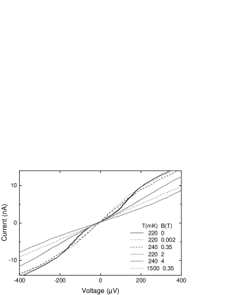
A possible explanation of the occurrence of such nonlinear IVs would be a strong enhancement of the critical field of a contact with high transmission values . A drastically enhanced critical field was observed previously for atomic-size contacts of Pb prepared with the help of an STM suderow in a magnetic field applied parallel to the current direction. It was attributed to the incomplete penetration of the magnetic field in narrow structures. In our previous measurements on Al contacts and Au contacts with Al leads fabricated with the same technique and field direction as the present experiments on Zn contacts, all signatures of superconductivity vanished at magnetic field values smaller than or equal to the bulk critical field of Al. However, in those samples the film structure was optically smooth. Accordingly, the granularity of the Zn film could be the reason for the unusually high critical, the nonlinearities only vanish at temperatures K, well above the critical temperature, which we estimate to be about 750 mK, since the signatures of MAR for atomic-contacts realized with the same sample disappear at this temperature.
Therefore and in accordance with the observed shift of the MAR peaks we attribute the nonlinearities to electron-interaction effects, such as Coulomb blockade, resonant tunneling or quantum interference effects. The interplay between electron-electron interaction effects and superconductivity in atomic-size structures has so far not been explored theoretically. Consequently, a detailed interpretation of the observed IVs below including the magnetic-field behavior is not possible.
Taking the typical voltage scale of the nonlinearities of V as a measure for the charging energy , we deduce a capacity fF corresponding to the capacity of a sphere with a diameter of 7 m. This value is about a factor 10 larger than the typical grain size of the Zn film. Thus, we interpret our observations to indicate the onset of the interaction effect. Due to the low-impedance environment of the circuit and the effective screening of the surrounding metal all interaction effects would be expected to be damped.
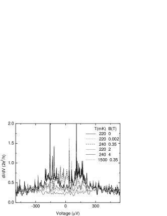
The numerical derivatives of the IVs of Fig.5, depicted in Fig. 6 show small, but reproducible fluctuations superimposed over the larger scale variations. The fluctuations have a typical voltage period of V, appear at the same voltage values for both sweep directions (but different for opposite sign of the voltage) and are correlated from curve to curve. These findings underline at first that the fluctuations are not due to experimental noise and second that the contact has not been changed by varying temperature and magnetic field. There are several possible origins of the fluctuations, including (universal) conductance fluctuations (CF) or again the onset of Coulomb blockade due to the granular structure of the film. The analysis in terms of CF yields a typical coherence length of nm roughly corresponding to the grain size of the evaporated film. A gradual transition from CF to Coulomb-blockade behavior has recently been observed in carbon nanotubes schoenenberger ; stojetz . However, the physical mechanism giving rise to this transition is not yet clear.
In conclusion, a single-atom contact of Zn is likely to have a conductance of . The histograms for both closing and opening the contacts indicate the importance of different contact geometries. In the IV characteristics in the superconducting state we find indications of interaction effects, perhaps due to the granular structure of the evaporated films. However, due to the lack of systematic measurements and theoretical investigations the interpretation of the features being due to a Coulomb-blockade type mechanism remains somewhat speculative.
I Acknowledgments
We acknowledge enlightening discussions with C. Urbina, D. Esteve and J. M. van Ruitenbeek. We have enjoyed fruitful interaction with J. C. Cuevas and we thank him for providing us with his computer codes. This work was supported by the Deutsche Forschungsgemeinschaft through SFB 195, SFB 513 and the Alfried Krupp von Bohlen und Halbach-Stiftung.
References
- (1) A. Avishai, A. Golub, A. D. Zaikin, Europhys. Lett. 54, 640.
- (2) N. Agraït, A. Levy Yeyati, and J. M. van Ruitenbeek, Physics Reports 377, 81 (2003).
- (3) R. Landauer, Phil. Magazine 21, 863 (1970)
- (4) A. I. Yanson and J. M. van Ruitenbeek, Phys. Rev. Lett. 79, 2157 (1997).
- (5) E. Scheer, P. Joyez, D. Esteve, C. Urbina, and M. H. Devoret, Phys. Rev. Lett 78, 3535 (1997).
- (6) H. E. van den Brom and J. M. van Ruitenbeek, Phys. Rev. Lett. 82, 1526 (1999).
- (7) R. Cron, M. F. Goffman, D. Esteve, and C. Urbina, Phys. Rev. Lett. 86, 4104 (1997).
- (8) B. Ludoph B, M. H. Devoret, D. Esteve, C. Urbina, and J. M. van Ruitenbeek, Phys. Rev. Lett. 82, 1530 (1999).
- (9) B. Ludoph and J. M. van Ruitenbeek, Phys. Rev. B 59, 12290 (1999).
- (10) M. F. Goffman, R. Cron, A. Levy Yeyati, P. Joyez, M. H. Devoret, D. Esteve, and Urbina, Phys. Rev. Lett. 85, 170 (2000).
- (11) D. A. Papaconstantopoulos, Handbook of the band structure of elemental solids, (Plenum Press, New York,1986).
- (12) E. Scheer, N. Agraït, J. C. Cuevas, A. Levy Yeyati, B. Ludoph, A. Martín-Rodero, G. Rubio Bollinger, J. M. van Ruitenbeek, and C. Urbina, Nature (London) 394, 154 (1998).
- (13) J. M. van Ruitenbeek, A. Alvarez, I. Piñeyro, C. Grahmann, P. Joyez, M. H. Devoret, D. Esteve, and C. Urbina, Rev. Sci. Inst. 67, 108 (1996).
- (14) C. Kittel, Introduction to solid state physics, 5th edition (Wiley, Chichester, 1976).
- (15) M. Dreher, J. Heurich, J. C. Cuevas, E. Scheer, and P. Nielaba, submitted to Phys. Rev. B and cond-mat/0406281.
- (16) M. Häfner, P. Konrad, F. Pauly, E. Scheer, and J. C. Cuevas, submitted to Phys. Rev. B (Rapid Communication)
- (17) A. I. Yanson, Atomic chains and electronic shells: quantum mechanisms for the formation of nanowires, PhD thesis, University of Leiden, The Netherlands, 2000.
- (18) B. Ludoph, N. van der Post,E. N. Bratus, E. V. Bezuglyi, V. S. Shumeiko, G. Wendin, and J. M. van Ruitenbeek, Phys. Rev. B 61, 8561 (2000).
- (19) J. L. Costa-Krämer, Phys. Rev. B 55, R4875 (1997).
- (20) E. Scheer, J. C. Cuevas, A. Levy Yeyati, A. Martín-Rodero, C. Urbina, P. Joyez, D. Esteve, and M. H. Devoret, Physica B 280, 425 (2000).
- (21) P. G. Tomlinson and J. C. Swihart, Phys. Rev. B. 19, 1892 (1979).
- (22) D. Averin and A. Bardas, Phys. Rev. Lett. 75, 1831 (1995).
- (23) J. C. Cuevas, A. Martín-Rodero, and A. Levy Yeyati, Phys. Rev. B 54, 7366 (1996).
- (24) E. Scheer, W. Belzig, Y. Naveh, M. H. Devoret, D. Esteve, and C. Urbina, Phys. Rev. Lett. 86, 284 (2001).
- (25) T. Böhler, J. Grebing, A. Mayer-Gindner, H. v. Löhneysen and E. Scheer, Nanotechnology 15, 465 (2004).
- (26) M. H. Devoret and and H. Grabert, (eds.) Single Charge Tunneling, NATO ASI Series B294 (Plenum, New York, 1992).
- (27) R. Cron, Atomic Contacts: a Test-Bed for Mesoscopic Physics, PhD thesis, University of Paris 6, France, 2001.
- (28) H. Suderow, E. Bascones, W. Belzig, F. Guinea, and S. Vieira, Europhys. Lett. 50, 749 (2000).
- (29) M. Buitelaar, T. Nussbaumer, and C. Schönenberger, Phys Rev. Lett. 89, 256801 (2002).
- (30) B. Stojetz, Verhandl. DPG (VI) 39 2/2004, 458 (2004).