Spectroscopy of Valley Splitting in a Silicon/Silicon-Germanium Two-Dimensional Electron Gas
Abstract
The lifting of the two-fold degeneracy of the conduction valleys in a strained silicon quantum well is critical for spin quantum computing. Here, we obtain an accurate measurement of the splitting of the valley states in the low-field region of interest, using the microwave spectroscopy technique of electron valley resonance (EVR). We compare our results with conventional methods, observing a linear magnetic field dependence of the valley splitting, and a strong low-field suppression, consistent with recent theory. The resonance linewidth shows a marked enhancement above mK.
pacs:
73.21.Fg,78.70.Gq,78.67.DeThe term “valley physics” refers to the study of degenerate valleys in the conduction band of an indirect gap semiconductor such as silicon. Valley physics has become a focal point in the field of silicon spintronics and quantum information processing because of the couplings between valley and spin states. For instance, in the Kane quantum computer kane98 , the interactions between spins are strongly modulated by interference between the different valleys koiller02 . Similar concerns exist for spin qubits in a quantum well eriksson04 .
Although valley physics has emerged as an important field of study, many important experimental questions remain unsettled, due to the dearth of valley-sensitive measurement techniques, particularly for a two dimensional electron gas (2DEG). One example is the discrepency between theory and experiment for the magnitude of the energy gap between the ground and excited valley states (the so-called valley splitting). While theory predicts that the valley splitting should be of order 1 meV for a silicon/silicon-germanium quantum well boykin04 , experimental measurements can be 10-100 times smaller weitz96 ; koester97 ; khrapai03 ; lai04 ; pudalov . Typical detection techniques involve beating in Shubnikov-de Haas measurements or activation energy analyses. These methods are difficult to apply with high precision, and they do not work well at the low fields of interest for quantum devices. Since valley splitting must be large enough to minimize excitations outside the qubit Hilbert space of a spin-based quantum computer friesen03 , it is crucial to understand the low-field valley physics, and to perform accurate low-field measurements.
In this Letter, we apply the high precision microwave resonance techniques developed for spin excitation to the problem of valley splitting in a 2DEG. Because of the small number of electrons and the low-temperature requirements, conventional microwave absorption spectroscopy techniques (which require almost 1012 electrons for an appreciable resonance signal jiang01 ) are difficult to employ in these structures. On the other hand, transport measurements are naturally suited for probing electrical characteristics of narrow channels containing relatively few carriers. Previous studies have combined these techniques in the form of electrically detected electron spin resonance (ED-ESR), thereby enabling the measurement of Zeeman splitting in both gallium arsenide jiang01 ; dobers88 ; dobers88b ; vitkalov00 ; olshanetsky03 and silicon graeff99 ; tyryshkin05 2DEG structures. Here, we show that electronic transitions can also be driven between the two lowest valley states using microwaves to achieve electrically detected electron valley resonance (ED-EVR). The advantage of this technique is that it allows accurate and dense data acquisition over more than a decade of low magnetic fields.
The Si/SiGe heterostructures used in these experiments were grown by ultrahigh vacuum chemical vapor deposition ismail95 . In each case, the 2DEG is located atop 80 Å of strained Si grown on a strain-relaxed Si0.7Ge0.3 buffer layer. The 2DEG is separated from the phosphorus donors by 140 Å of Si0.7Ge0.3. The donors lie in a 140 Å layer of Si0.7Ge0.3 with a 35 Å Si cap at the surface. Further details about the structure can be found in reference klein04 . Two 2DEGs ( and ) were measured at 0.25 K, obtaining the electron densities () and (), and the mobilities /Vs () and /Vs ().
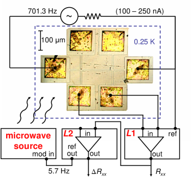
A schematic of the experimental set-up is shown in Fig. 1. A double lock-in technique is used to measure the change in resistance of the 2DEG as a function of the perpendicular field , in the presence of microwaves. Lock-in 1 provides a bias current ranging from 100 nA to 250 nA, modulated at 701.3 Hz. Lock-in 2 is used to modulate the microwave amplitude with 100% modulation at 5.7 Hz. The output of Lock-in 1 is fed into Lock-in 2, which measures . Microwaves are produced by an HP83650A synthesizer, and are carried down to the sample using a low loss coaxial line terminating about 5 cm from the surface of the sample in a loop antenna. The base of a resonant cavity is replaced with a sample stage. The microwave power at the sample has a strong frequency dependence because of the open cavity and the impedence mismatches along the length of the coaxial line. Because of this non-uniformity, a wide range of powers (10 W-10 mW) are used to ensure optimal power delivery. The magnetic field is produced by a superconducting magnet and all measurements are carried out in an Oxford Instruments 3He cryostat with a base temperature of 0.25 K.
The same experimental set-up can be used to detect both ESR and EVR signals. Although we do not report on ESR here, we observe typical resonances, with linewidths on the order of 5 G for and 2 G for . The EVR transition is slightly different than ESR because it is not driven by magnetic fields. (The two low-lying valley states are orthogonal and unaffected by the spin operator, causing the Zeeman transition matrix element to vanish.) However, the electric dipole transition is allowed by general symmetry considerations kleiner , which also apply to the quantum well geometry. We can estimate the magnitude of this valley excitation using a one-dimensional tight binding (TB) method boykin04 . Since the two valley states differ only along the direction (the direction perpendicular to the quantum well), only the component of the microwave field may induce transitions. The resulting dipole matrix element is rather small. Nonetheless, it is the dominant transition mechanism. By further positioning the sample at or nodes in the resonant cavity, it may be possible to drive valley or spin excitations selectively, although we do not perform such experiments here.
Shubnikov-de Haas oscillations provide a rough estimate of the valley splitting, as demonstrated in the inset of Fig. 2 for sample . Both spin and valley features can be observed in the data lai04 . By increasing the magnetic field, we observe a sequential removal of the spin and valley degeneracies, as indicated by the appearance of split spin and valley peaks. In the main figure, we present a measurement of the valley splitting (circles), based on an activation energy analysis weitz96 . The analysis provides results only at higher magnetic fields. The larger error bars reflect uncertainties in the fitting of the activation data, similar to previous experiments weitz96 .
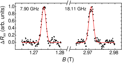
In contrast, the electrically-detected EVR measurement provides narrow error bars, and covers a wide range of magnetic fields. Here, we obtain data from 0.27 T to 3 T on sample , with narrow error bars throughout. Some typical resonances are shown in Fig. 3. To analyze the resonance features, we fit the data. First, the background resistance is removed by fitting to a second degree polynomial away from the main peak. We find that gaussians provide the best representation of the individual peaks, with peak widths on the order of 20-25 G. Typically, the resonance features account for about one part in of the total resistance signal. In Fig. 3, the the peak heights have been scaled to unity.
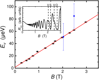
The fitted peak positions are plotted in Fig. 2 (squares), as a function of the perpendicular magnetic field. To estimate the error bars, we note that the microwave power dependence of the resonance peak shows a shift towards higher fields with increasing power. The largest observed shift is about 100 G over two orders of magnitude in the power. In the figure, we determine our error bars using a more generous estimate of 500 G. The resulting data are strikingly linear, with regression giving a slope of , and a -intercept of . A separate linear fit of the valley splitting data from suggests a slightly larger slope for . Although this fit has larger error bars than the EVR analysis, the results appear consistent with theoretical expectations that the valley splitting should scale with the 2DEG density as theory .
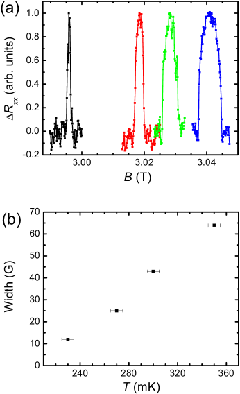
Figure 4 shows the effect of temperature on the resonance peaks. We use the frequency (18.11 GHz) and magnetic field (3.0 T) that give the largest valley splitting. Data sets are taken as the sample temperature is increased from 0.23 K to 0.35 K and decreased back to 0.23 K at a slow rate, giving the sample enough time to equilibriate. The error bars for Fig. 4(b) are obtained from the hysteresis in peak widths during the temperature cycle. Over this narrow temperature range there is a sudden, rapid (seven-fold) increase in the linewidth. Resonances at higher temperatures are difficult to observe, although valley splitting can still be observed in the activation energy analysis, for temperatures up to 1 K. In addition to thermal broadening of the resonance, we also observe a small but reproducible increase in the peak position of about 400 G, or 1.5%, indicating a small thermal enhancement of the valley splitting.
While the data in Fig. 2 are internally consistent, they give values for valley splitting that are far smaller than the theoretical estimates. In the conventional theory of valley splitting, the degeneracy of the conduction valleys is broken by the sharp confinement potential of the quantum well, which couples the valleys in space ohkawa77 ; sham79 ; AFS . Tight binding and non-equilibrium Green’s functions techniques obtain estimates of 0.1-1 meV for the valley splitting, depending on the quantum well width and the internal electric field associated with modulation doping boykin04 . It has been suggested that the magnetic field dependence arises from the enhancement of exchange coupling due to electron-electron interactions in the 2DEG ohkawa77 ; AFS ; shkolnikov02 . However, the many-body effect is expected to enhance the valley splitting, in contrast with the suppression observed in experiments. In addition, the linear dependence of is inconsistent with the expected scaling for the many-body theory shkolnikov02 .
Ando has proposed an alternative explanation for the suppression of valley splitting AFS ; ando79 . In this picture, the sharp confinement potential is still the cause of the valley splitting. However, one must also include the effects of substrate miscut and rough growth surfaces. Indeed, the commercial substrates used for SiGe heterostructures are often purposely miscut. The samples used in this work were miscut at a angle. Quantum wells grown on such substrates will be misaligned with respect to the crystallographic axes. For rough surfaces, there will be an additional, locally varying misalignment.
A theory of valley splitting on a stepped quantum well is given in Ref. theory , based on effective mass theory. A number of the experimental features in Fig. 2 appear consistent with the theoretical predictions. We now briefly discuss the theory, and its implications for our work. The valley splitting can be expressed as a simple integral, , where is the position of the valley minimum, is the effective mass envelope function, and is a valley coupling interaction, caused by the sharp interface of the quantum well. Each step in the quantum well makes a contribution to the integral with the phase , where is the interface position of the th step. Since the difference in the phase angles on consecutive steps is , where Å is the atomic step height, the step contributions interfere destructively. Thus, an electronic wavefunction covering many steps will have a valley splitting that is strongly suppressed compared to the flat quantum wells of Ref. boykin04 . Since stepped surfaces are ubiquitous in conventional semiconductor heterostructures, so too is the suppression of the valley splitting. In a magnetic field, on the other hand, the electron is confined to a finite number of steps, thereby limiting the destructive interference. For very large magnetic fields, the electron may be confined to a single step. In this limit, the valley splitting is restored, and achieves its theoretical upper bound.
The arguments given in Ref. theory for the strong suppression of at very low fields are plausible and consistent with our data. The partial lifting of this suppression due to step disorder and other fluctuations is also plausible. In Ref. theory , simulations were performed on disordered steps, including bunched steps. These obtain valley splitting results very close, quantitatively, to the data of Fig. 2. However, the shape of the curves obtained from the simulations depends on the particular disorder model, making a definite theoretical comparison difficult. Most noteably, the simulation results do not appear completely linear, contrary to our experimental observations. A particular “plateau” model was suggested in that work, as an example of a disorder model producing a linear . However, experimental verification of such behavior is not yet available. On the other hand, the proposed model of envelope function oscillations at gives an estimate for the valley splitting which is very close to the extrapolated of value for , obtained from Fig. 2.
There are other open questions in the valley splitting theory of Ref. theory . The EVR experiments summarized in Figs. 2 and 3 exhibit sharp resonance peaks, indicating a well-defined valley splitting. However, models involving disorder suggest that electrons can become localized in the valley splitting landscape. In this picture, electrons may fill both shallow and deep pinning sites, consistent with a range of valley splittings. One might therefore expect a broad resonance peak, in contrast with experimental observations. It is tempting to attribute the marked thermal broadening of the EVR peaks to the increased occupation of higher energy states. A more complete theory must also take into account the fact that our electrical detection method is inherently dynamical.
Finally, we discuss the importance of our results for quantum computing in a silicon 2DEG. To minimize the excitation of the valley states in a spin-based quantum computer, the valley splitting should be much larger than the temperature. For a system cooled to 100 mK, a valley splitting of 100 eV should be adequate. We have noted that a strongly confined electron will exhibit a larger valley splitting. For the plateau model of Ref. theory , the linear dependence of can be expressed through , where is the miscut angle, and is the rms radius of the magnetically confined wavefunction. We can extend this scaling to confinement produced by gate potentials. For sample , with , our experimental results lead to . If we now take to be the quantum dot radius and require eV, we obtain the relation nm. To attain eV on a miscut therefore requires a fairly small dot radius of 18 nm. However, for a miscut, a larger 120 nm dot can be used.
In conclusion, we have performed microwave spectroscopy of the conduction valley states in a strained silicon 2DEG using transport measurements. Our method provides a measurement of the valley splitting over a wide range of relatively low magnetic fields (0.3-3 T). We also obtain temperature dependent measurements showing a strong change in the valley splitting behavior above 300 mK. We compare our data to a recent theory of valley splitting on a stepped substrate obtaining quantitative agreement, but leaving some open questions.
Acknowledgements.
We gratefully acknowledge conversations with R. Blick. This work was supported by NSA and ARDA under ARO contract number W911NF-04-1-0389, and by the National Science Foundation through the ITR program (DMR-0325634) and the QuBIC program (EIA-0130400).References
- (1) B. E. Kane, Nature (London) 393, 133 (1998).
- (2) B. Koiller, X. Hu, and S. Das Sarma, Phys. Rev. Lett. 88, 027903 (2001).
- (3) M. A. Eriksson, et al., Quant. Inform. Process. 3, 133 (2004).
- (4) T. B. Boykin, et al., Appl. Phys. Lett. 84, 115 (2004); Phys. Rev. B70, 165325 (2004).
- (5) P. Weitz, et al., Surface Science 361/362, 542 (1996).
- (6) S. J. Koester, K. Ismail, and J. O. Chu, Semicond. Sci. Technol. 12, 384 (1997).
- (7) V. S. Khrapai, A. A. Shashkin, and V. P. Dolgopolov, Phys. Rev. B67, 113305 (2003).
- (8) K. Lai, et al., Phys. Rev. Lett. 93, 156805 (2004).
- (9) V. M. Pudalov et al., cond-mat/0104347.
- (10) M. Friesen, et al., Phys. Rev. B67, 121301 (2003).
- (11) H. W. Jiang and Eli Yablonovitch, Phys. Rev. B64, 041307 (2001).
- (12) M. Dobers, K. von Klitzing, and G. Weimann, Phys. Rev. B38, 5453 (1988).
- (13) M. Dobers, K. von Klitzing, J. Schneider, G. Weimann, and K. Ploog, Phys. Rev. Lett. 61, 1650 (1988).
- (14) S. A. Vitkalov, C. R. Bowers, J. L. Simmons, and J. L. Reno, Phys. Rev. B61, 5447 (2000).
- (15) E. Olshanetsky et al., Phys. Rev. B67, 165325 (2003).
- (16) C. F. O. Graeff et al., Phys. Rev. B59, 13242 (1999).
- (17) A. M. Tyryshkin, S. A. Lyon, W. Jantsch and F. Schaeffler, Phys. Rev. Lett. 94, 126802 (2005).
- (18) K. Ismail, M. Arafa and K. L. Saenger, Appl. Phys. Lett. 66, 1077 (1995).
- (19) L. J. Klein et al., Appl. Phys. Lett. 84, 4047 (2004).
- (20) W. H. Kleiner and W. E. Krag, Phys. Rev. Lett. 25, 1490 (1970).
- (21) M. Friesen, M. A. Eriksson, and S. N. Coppersmith, unpublished.
- (22) F. J. Ohkawa and Y. Uemura, Journ. Phys. Soc. Japan, 43, 925 (1977).
- (23) L. J. Sham and M. Nakayama, Phys. Rev. B20, 734 (1979).
- (24) T. Ando, A. B. Fowler, and F. Stern, Rev. Mod. Phys. 54, 437 (1982).
- (25) Y. P. Shkolnikov, E. P. De Poortere, E. Tutuc, and M. Shayegan, Phys. Rev. Lett. 89, 226805 (2002).
- (26) T. Ando, Phys. Rev. B19, 3089 (1979).