Inelastic electron tunneling via molecular vibrations in single-molecule transistors
Abstract
In single-molecule transistors, we observe inelastic cotunneling features that correspond energetically to vibrational excitations of the molecule, as determined by Raman and infrared spectroscopy. This is a form of inelastic electron tunneling spectroscopy of single molecules, with the transistor geometry allowing in-situ tuning of the electronic states via a gate electrode. The vibrational features shift and change shape as the electronic levels are tuned near resonance, indicating significant modification of the vibrational states. When the molecule contains an unpaired electron, we also observe vibrational satellite features around the Kondo resonance.
pacs:
73.22.-f,73.23.-b,73.23.HkElectron tunneling is widespread throughout chemistry and condensed matter physics. Electron transfer through molecules by nonresonant tunneling has long been knownMarcus56JCP ; McConnell61JCP , and tunneling electrons can interact inelastically with molecules, exciting vibrational modes. This is the basis of inelastic electron tunneling spectroscopy (IETS)JaklevicetAl66PRL ; HippsetAl93JPC , recently refined to probe groups of molecules via crossed wiresGregory90PRL ; ZimmermanetAl01RSI ; KushmericketAl04NL and nanoporesWangetAl04NL , and single molecules via scanning tunneling microscopy (STM)StipeetAl98Science . Similar inelastic, nonresonant tunneling occurs in single-electron transistors (SETs)Averinbook ; DeFranceschietAl01PRL , three-terminal devices in which a gate electrode allows in-situ adjustment of the energy levels. To date, this tuning has not been possible in the chemical systems examined by IETS.
In this Letter we report inelastic cotunneling processes in single-molecule transistors (SMTs)ParketAl00Nature ; ParketAl02Nature ; LiangetAl02Nature ; YuetAl04NL , and identify them with vibrational excitations of the molecules, as determined by Raman and infrared spectroscopy. Tuning electronic levels near resonance reveals shifts in inelastic lineshapes and peak positions, suggesting significantly modified electron-vibrational coupling in this region. The vibrational features persist in the Kondo regime, indicating a complicated conduction process involving vibrational excitations of a many-body electronic system.
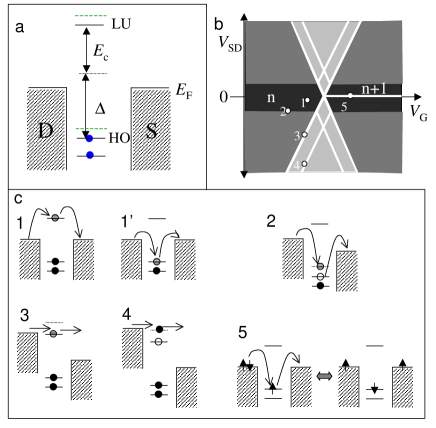
A confined electronic system (“island”) coupled by tunneling to source and drain electrodes is shown schematically in Fig. 1a. The energy to promote an electron from the highest occupied (HO) to the lowest unoccupied (LU) orbital is the single-particle level spacing, . Ignoring spin, adding an electron to the island also requires additional Coulomb ”charging energy”, , often approximated in SETs by the charging energy of a classical capacitor. In molecules, a manifold of vibrational excitations is associated with each electronic state. In a three-terminal device, the island levels may be shifted via a gate potential. Fig. 1b maps the differential conductance, , of a generic SET as a function of source-drain bias, , and gate voltage, , while Fig. 1c shows possible electronic transport mechanisms. For low biases (Fig. 1c, 1,1’) the average number of electrons on the island is fixed; transport is suppressed (Coulomb blockade) and can only occur by higher order tunneling through virtual states. An example of this in chemical electron transfer is “superexchange”McConnell61JCP , and in SETs such processes are called “elastic cotunneling”Averinbook . At higher biases in the blockaded regime, “inelastic cotunneling” via an excited virtual state (Fig. 1c, 2) is possible. For an excitation of energy , the opening of the inelastic channel results in a feature in at . Inelastic cotunneling via electronically excited states has been seen in semiconductorDeFranceschietAl01PRL and carbon nanotube SETsLiangetAl02PRL . Inelastic cotunneling via vibrationally excited molecules is responsible for conventional IETSTroisietAl03JCP , but has not been studied in three-terminal devices. IETS lineshapes are predicted to vary significantly depending on the energetics of the virtual statesGalperinetAl04condmat , and can be peaks, dips, or intermediate structures in . At still higher source-drain biases (Fig. 1c, 3) Coulomb blockade is lifted leading to significant resonant conduction, while at still higher biases (Fig. 1c, 4) additional resonant conduction occurs when is sufficient to leave the island in an electronicallyJohnsonetAl92PRL ; StewartetAl97Science ; KouwenhovenetAl97Science or vibrationallyParketAl00Nature ; ParketAl02Nature ; YuetAl04NL ; QiuetAl04PRL excited state.
When the effects of unpaired spins are included, the Kondo resonance becomes a possible conduction mechanism, and is detected as a sharp conductance peak near zero biasGoldhaberGordonetAl98Nature ; CronenwettetAl98Science at temperatures low compared to a characteristic energy scale, . The maximum peak conductance possible is , for a system with perfectly symmetric coupling between the island and the source and drain electrodes. Kondo physics has been observed recently in single-molecule transistorsParketAl02Nature ; LiangetAl02Nature ; YuetAl04NL .
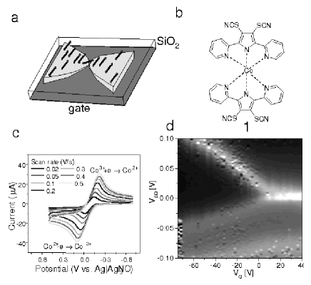
Single-molecule transistors open the possibility of examining inelastic cotunneling in individual, tunable chemical systems, in both the blockaded and Kondo regimes. We fabricate SMTs (Fig. 2a) using an electromigration method that has been described extensivelyParketAl00Nature ; ParketAl02Nature ; LiangetAl02Nature ; YuetAl04NL . The source and drain electrodes are 15 nm Au films with 1 nm Ti adhesion layers, prepared by electron beam lithography, e-beam evaporation, liftoff, and oxygen plasma cleaning. The gate oxide is 200 nm SiO2, with a degenerately doped Si (100) wafer as the underlying gate electrode. While this thickness of oxide guarantees relatively weak gate couplings due to simple geometric considerations, we routinely obtain excellent device reliability up to gate fields of V/m with negligible leakage.
The starting molecule, 1, (Fig. 2b) comprises a single transition metal ion (Co2+) coordinated by conjugated ligands; the valence state of the ion may be controlled electrochemically (Fig. 2c). The structure of 1 has been verified by x-ray crystallography. Compound 1 undergoes loss of the (CN) moieties upon assembly on gold in tetrahydrofuran (THF), yielding the corresponding di- or tri-thiolate, which is bound covalently to surface Au atomsCiszeketAl04JACS . Both 1 and its self-assembly have been characterized extensively by x-ray photoemission, ellipsometry, and electrochemical methodssupp .
A 2mM solution of 1 in THF is allowed to self-assemble on the electrode sets for 48 hours. The chip is then rinsed in THF, dried in a nitrogen stream, and placed in a variable temperature vacuum probe station (Desert Cryogenics). This cryostat does not have magnetic field capabilities, but does permit characterization of many junctions at once. The junctions are partially broken to the k level by electromigration at room temperature, cooled to liquid helium temperatures, and broken by further electromigration into separate source and drain electrodes.
At a variety of temperatures, we have measured as a function of at from -100 V to +100 V using a semiconductor parameter analyzer (HP4145B), with the source grounded and the drain electrode swept. We compute the differential conductance and as a function of and by numerical differentiation. Spot comparisons between this approach and lock-in techniques show excellent agreementsupp . To avoid artifacts we identify features in by comparing multiple data sets taken at the same or nearby gate voltages.
We have examined 407 electrode pairs on 10 separate substrates, with statistics similar to those in previous investigationsYuetAl04NL . Of the electrode pairs examined we found 57 devices with no detectable current (electrodes too far apart for measurable conduction); 166 with linear, nongateable current-voltage characteristics (likely no molecule present at the junction); 108 with nonlinear but ungateable current-voltage characteristics (either molecules or metal nanoparticles with negligible gate coupling); and 76 nonlinear but significantly gateable current-voltage characteristics. From this last group, four were identified as single-electron devices based on unintentionally produced metal nanoparticles. This identification was based on the observation of many regularly spaced Coulomb blockade regions with typical electron addition energies less than 50 meV. In working devices, bias sweeps were restricted to mV to minimize the chances of current-induced irreversible changes. Device stability is poor at high current densities and temperatures significantly above 4.2 K, likely due to the atomic diffusion of the Au electrode material.
There are 27 devices that cleanly display a single Coulomb degeneracy point, the vast majority of which show a resonance at zero in one charge state identified as a Kondo resonance, as in Fig. 2d. Control devices with electrodes exposed to THF without 1 never display such conductance properties. As can be seen from the edges of the Coulomb blockade region, the electron addition energy for the device in Fig. 2d exceeds 100 meV; this is typical. The Kondo properties are very similar to those reported in earlier SMTs based on Co2+-containing complexesParketAl02Nature . Typical Kondo temperatures as inferred from the temperature dependence of the Kondo resonance height and the low temperature width of the resonance are 40 K. The low temperature limit of the resonance peak height is often reduced from the theoretical maximum value of , indicating asymmetric coupling of the molecule to the source and drain electrodes. A full discussion of Kondo physics in 1 and related molecules will be reported elsewhere.
In 12 devices, the conductance in the classically blockaded region and/or outside the Kondo resonance is large enough to allow clean measurements of . In Figs. 3, we show maps of this quantity as a function of and in two different devices at 5 K. We have indicated two prominent features within the blockaded (Kondo) regime with black arrows. Features in of opposite sign are symmetrically located around zero source-drain bias, consistent with features expected from inelastic tunneling. Some asymmetry in shape is unsurprising, given that the low peak conductance in the Kondo regime for these devices indicates significantly asymmetric coupling of the molecule to the leads.
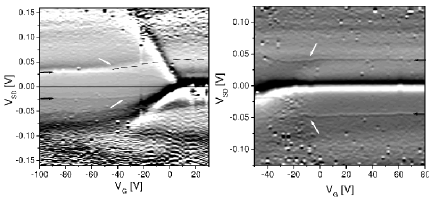
The features in the blockaded region occur at essentially constant values of until is varied such that the feature approaches the edge of the blockaded region. This constancy in has been identified as a feature of inelastic cotunneling in semiconductorDeFranceschietAl01PRL and nanotubeLiangetAl02PRL single-electron devices. The changes in these features as the boundaries of the Coulomb stability region are crossed indicate that the inelastic processes are native to the SMT itself, and not due to some parallel conduction channel. The inelastic modes occur at energies low compared to (100s of meV), implying that the modes being excited are unlikely to be electronic. By examining the data for features at fixed as a function of , we identified a total of 43 candidate inelastic features at meV, ranging in apparent width from 5 mV to 20 mV at 5 K. The narrowest inelastic features clearly show a broadening as the temperature is elevated above 20 K. Further studies will seek to compare this broadening with standard theoretical treatments of linewidths in IETS.
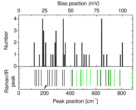
Fig. 4 shows a histogram (bin = 1 mV) of the positions of those features, from detailed examination of vs. data. The lower panel shows Raman (Stokes) peak positions (data taken on a powder of 1) and IR absorption peak positions of 1 (in pellet form, blended with KBr)supp . The correlations between the spectra and inelastic features in confirm that vibrational inelastic cotunneling processes are at work in the molecular transistors. This is consistent with the observation of IETS in single molecules by STMStipeetAl98Science . The fact that different SMTs exhibit different subsets of features is a natural consequence of the sensitivity of IETS to the nanoscale structure of the molecular junctionChenetAl04condmat . Comparisons with Raman of 1 and related compounds (e.g. ligands without -SCN; ligands without Co2+) suggest tentative peak assignments. The peaks near 36 meV and 55 meV are likely the Co-N stretchSocratesbook , while that near 44 meV is tentatively a -SCN deformationSocratesbook (implying that not every S is bonded to an Au surface atom, consistent with x-ray photoemission datasupp ). The 24 meV peak is tentatively the Au-S bondKatoetAl02JPCB ; this claim is further supported by the appearance of a 28 meV Raman peak in films of 1 assembled on Au electrodes, while such a peak is absent in Raman spectra of both unassembled 1 and bare electrodes.
As indicated by white arrows in Fig. 3, inelastic features shift and change near the boundary of the Coulomb blockade region. These changes as a function of are qualitatively consistent with recent theoretical expectationsGalperinetAl04condmat , though detailed modelling would be required for quantitative comparisons. The energy of the virtual cotunneling states is shifted by , altering the (complex) amplitude for that process. Changing the cotunneling amplitude compared to quasi-elastic (with the virtual excitation and readsorption of a vibrational quantum) or direct source-drain tunneling is predicted to severely alter lineshapes. These effects cannot be examined in two-terminal tunneling structures, which lack the ability to shift the relevant virtual states. We note that occasionally inelastic features shift significantly in energy as the blockade boundary is approached (e.g. the 24 meV features in Fig. 3(left)). This would be consistent with a modified (dressed) electron-vibrational coupling near the electronic resonance.
We observe that the IETS features persist into the Kondo regime in the form of satellite features paralleling the zero-bias Kondo resonance. Often specific features may be traced from the blockaded region into the Kondo region, an example of which is indicated by the dashed line in Fig. 3(left). Through the transition the inelastic feature lineshapes change, as do their intensities. Such inelastic satellites paralleling the Kondo resonance have been suggested previouslyLiangetAl02Nature ; YuetAl04NL , and the consistency in feature position in our data lend strong support to this idea. Recent experiments in semiconductor devicesKoganetAl04Science have demonstrated the existence of satellite Kondo peaks when the Kondo system can interact inelastically with photons of a well defined energy. In the molecular transistor case, the inelastic exchange occurs with the vibrational quanta of the molecule, demonstrating a quantum mechanically coherent coupling between the electronic many-body Kondo state, and the mechanical resonances of the molecule. These Kondo measurements illustrate how the tunability of single-molecule transistors permits the examination of vibrational processes as a function of the energetics of the electronic levels, a study not possible in standard two-terminal devices.
The authors thank A. Nitzan and M. Di Ventra for useful discussions. DN acknowledges financial support from the Research Corporation, the Robert A. Welch Foundation, the David and Lucille Packard Foundation, an Alfred P. Sloan Foundation Fellowship, and NSF award DMR-0347253. JMT acknowledges support from DARPA and the ONR.
References
- (1) R.A. Marcus, J. Chem. Phys. 24, 966 (1956).
- (2) H.M. McConnell, J. Chem. Phys. 35, 508 (1961).
- (3) R.C. Jaklevic and J. Lambe, Phys. Rev. Lett. 17, 1139 (1966).
- (4) K.W. Hipps and U. Mazur, J. Phys. Chem. 97, 7803 (1993).
- (5) S. Gregory, Phys. Rev. Lett. 64, 689 (1990).
- (6) D.T. Zimmerman and G. Agnolet, Rev. Sci. Instr. 72, 1781 (2001).
- (7) J.G. Kushmerick, J. Lazorcik, C.H. Patterson, R. Shashidar, D.S. Seferos, and G.C. Bazan, Nano Letters 4, 639 (2004).
- (8) W.Y. Wang, T. Lee, I. Kretschmar, and M.A. Reed, Nano Letters 4, 643 (2004).
- (9) B.C. Stipe, M.A. Rezaei, and W. Ho, Science 280, 1732 (1998).
- (10) D.V. Averin and Y.V. Nazarov, in Single Charge Tunneling: Coulomb Blockade Phenomena in Nanostructures, H. Grabert and M.H. Devoret, eds. (Plenum, New York, 1992), 217.
- (11) S. De Franceschi, S. Sasaki, J.M. Elzerman, W.G. van der Wiel, S. Tarucha, and L.P. Kouwenhoven, Phys. Rev. Lett. 86, 878 (2001).
- (12) H. Park, J. Park, A.K.L. Lim, E.H. Anderson, A.P. Alivisatos, and P.L. McEuen, Nature 407, 57 (2000).
- (13) J. Park, A.N. Pasupathy, J.I. Goldsmith, C. Chang, Y. Yaish, J.R. Petta, M. Rinkowski, J.P. Sethna, H.D. Abruña, P.L. McEuen, and D.C. Ralph, Nature 417, 722 (2002).
- (14) W. Liang, M.P. Shores, M. Bockrath, J.R. Long, and H. Park, Nature 417, 725 (2002).
- (15) L.H. Yu and D. Natelson, Nano Letters 4, 79 (2004).
- (16) W.J. Liang, M. Bockrath, and H. Park, Phys. Rev. Lett. 88, 126801 (2002).
- (17) A. Troisi, M.A. Ratner, and A. Nitzan, J. Chem. Phys. 118, 6072 (2003).
- (18) M. Galperin, M.A. Ratner, and A. Nitzan, Nano Letters, 4, in press (2004); M. Galperin, M.A. Ratner, and A. Nitzan, cond-mat/0405343 (2004).
- (19) A.T. Johnson, L.P. Kouwenhoven, W. deJong, N.C. vanderVaart, C.J.P.M. Harmans, and C.T. Foxon, Phys. Rev. Lett. 69, 1592 (1992).
- (20) D.R. Stewart, D. Sprinzak, C.M. Marcus, C.I. Duruoz, and J.S. Harris, Science 278, 1784 (1997).
- (21) L.P. Kouwenhoven, T.H. Oosterkamp, M.W.S. Danoesastro, M. Eto, D.G. Austing, T. Honda, S. Tarucha, Science 278, 1788 (1997).
- (22) X.H. Qiu, G.V. Nazin, and W. Ho, Phys. Rev. Lett. 92, 206102 (2004).
- (23) D. Goldhaber-Gordon, H. Shtrikman, D. Mahalu, D. Abusch-Magder, U. Meirav, and M.A. Kastner, Nature 391, 156 (1998).
- (24) S.H. Cronenwett, T.H. Oosterkamp, and L.P. Kouwenhoven, Science 281, 540 (1998).
- (25) J.W. Ciszek, M.P. Stewart, J.M. Tour, submitted (2004).
- (26) See EPAPS Document No. YYY for discussion of molecule characterization, self-assembly, and measurement technique. A direct link to this document may be found in the online article’s HTML reference section. The document may also be reached via the EPAPS homepage (http://www.aip.org/pubservs/epaps.html) or from ftp.aip.org in the directory /epaps/. See the EPAPS homepage for more information.
- (27) Y.-C. Chen, M. Zwolak, and M. Di Ventra, cond-mat/0402536 (2004).
- (28) G. Socrates, Infrared and Raman Characteristic Group Frequencies: Tables and Charts, 3rd ed. (Wiley, New York, 2001), 347.
- (29) H.S. Kato, J. Noh, M. Hara, and M. Kawai, J. Phys. Chem. B 106, 9655 (2002).
- (30) A. Kogan, S. Amasha, and M.A. Kastner, Science 304, 1293 (2004).