Occurrence of Hysteresis like behavior of resistance of film in heating-cooling cycle.
P. Arun 111arunp92@physics.du.ac.in, Pankaj Tyagi &
A. G. Vedeshwar 222agni@physics.du.ac.in∗
Department of Physics & Astrophysics,
University of Delhi, Delhi - 110 007,
India
Abstract
Experimental observations of a peculiar behavior observed on heating and
cooling films at different heating and cooling rate are
detailed. The film regained its original resistance, forming a closed loop,
on the completion of the heating-cooling cycle which was reproducible
for identical conditions of heating and cooling. The area enclosed by the
loop was found to depend on (i) the thickness of the film, (ii) the heating
rate, (iii) the maximum temperature to which film was heated and (iv) the
cooling rate. The observations are explained on basis of model which
considers the film to be a resultant of parallel resistances. The film’s
finite thermal conductivity gives rise to a temperature gradient along the
thickness of the film, due to this and the temperature coefficient of
resistance, the parallel combination of resistance changes with temperature.
Difference in heating and cooling rates give different temperature gradient,
which explains the observed hysteresis.
PACS: 73.61.Le
1 Introduction
The electrical conductivity measurement is quite an important characterization technique for thin films and are routinely carried out for various materials ranging from metals to high resistive semiconductors. The temperature dependence of resistivity yields information about intrinsic band gap of material, activation energy for conduction in polycrystalline films (grain boundary barrier height), impurity activation energy etc. In most of these measurements data are taken either in heating or cooling direction of temperature variation. If the system is homogeneous and the rate of change of temperature is constant, no hysteresis can be expected in heating-cooling cycle. However, considerable hysteresis has been observed when an amorphous film was heated above crystalline transition temperature and cooled back which can be understood as due to structural changes [1, 2, 3]. Such hysteresis have been observed in Bi films even without structural changes [4]. A hysteresis behavior was also observed in Pd film which was ascribed to absorption and desorption of hydrogen during heating-cooling cycle [5]. Therefore, it motivated us to investigate more thoroughly the temperature dependence of electrical resistance in heating- cooling cycles for film in vacuum. We report here the interesting observations of hysteretic behavior in repeated cycles of heating- cooling. The results can be explained by the parallel resistor model [6].
2 Experimental Details
Thin films of were grown by thermal evaporation using a molybdenum boat on microscope slides glass substrates at room temperature at a vacuum better than Torr. The starting material was 99.99% pure stoichiometric ingot supplied by Aldrich (USA). Films were grown on the pre-deposited indium contacts using a mask for the four probe configuration of resistivity measurements. The electrical constacts were confirmed to be ohmic for all the samples studied. The temperature of the film was measured by a thermocouple placed very near to the sample on the substrate. The structure, chemical composition and morphology of the films were determined by X-ray diffraction (Philip PW1840 X-ray diffractometer), photo-electron spectroscopy (Shimadzu’s ESCA 750) and scanning electron microscope (JOEL-840) respectively. The film thickness was monitored during it’s growth by quartz crystal thickness monitor and was subsequently confirmed by Dektak IIA surface profiler, which uses the method of a mechanical stylus movement on the surface. The movement of the stylus across the edge of the film determines the step height or the film thickness. All the films were found to be stoichiometric and micro-crystalline after they were allowed to age in vacuum for few weeks [7]. Various films of thickness between 100 to 500nm were used during the experiment. All the heating-cooling cycles for resistivity measurements were carried out in vacuum of about Torr. This was done to prevent any oxidation of the films while heating, which would result in an irreversible change in the film resistance. The samples were heated by placing them on a copper block which is heated by a heating coil embedded in it.
The heating rate was varied by the voltage applied to the heating coil. The temperature and the resistance of the film was measured as a function of time. The heater was switched off for cooling the film. The cooling of the film from its elevated temperature was very slow as the measurements were done in vacuum. Therefore, while some control of the heating rate was maintained by controlling the voltage applied to the heating coil, the cooling rate was essentially determined by the maximum temperature at which the heater was switched off. The heating and cooling rates hence, were largely different.
Figure 1 shows the variation of temperature with time for both heating and cooling cycles. The temperature increases with time as indicated in segment ”AB”. The heater was switched off on attaining the pre-determined temperature. Point ”B” corresponds to the instant the heater was switched off. This is followed by a period of constant temperature ”BC”. The onset of cooling process starts at point ”C”. The cooling of the films in vacuum could be either by radiation losses or by conduction through the substrate side or both. After the heater is switched off, since the process is in vacuum, the substrate temperature remains constant for an appreciably long time before it starts falling. From figure 1, we find that the fall in substrate temperature commences 200sec later ater the heater is switched off. Beyond point ‘C’ the cooling process starts. However, as explained earlier, since the cooling process takes place in vacuum, it is very slow, hence the figure does not show the attainment of room temperature on cooling. Data of region ”AB” is best fitted by the equation
| (1) |
The equation shows saturation of temperature with time when the heating due to the heater is compensated by cooling. is the room temperature. The magnitude of and ”Q” are related in a complex manner to the heater voltage, cooling mechanism etc. An estimate of these factors are made by fitting equation (1) to the experimental data shown in figure 1. The value of coefficients , ”Q” and were estimated as 360oC, 0.00039 and 14.5oC respectively. From equation (1), the rate of heating during the heating cycle is given by
| (2) |
Similarly, the cooling rate can be found by fitting data of the cooling region by the equation
| (3) |
where is the final temperature attained before the heater is switched off. In the present work . The cooling rate is governed by ”S” and in our case since cooling was occurring naturally in vacuum (Torr), ”S” was very low 0.00021.
3 Results and Discussions
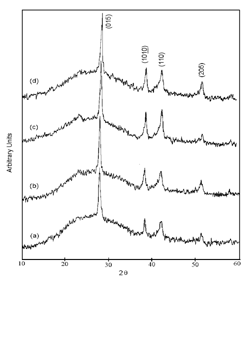
The resistance of as grown film was found to be high and decreases with time saturating in a few weeks [7]. No further change in resistance was observed with time thereafter. The as grown amorphous films were found to age into a polycrystalline state, with peak positions matching those given in ASTM card 15-874. The film resistance follows a hysteresis path with heating-cooling cycle which was reproducible under identical conditions. Reproducibility was tested as many as 20 times in some samples. The films were heated to various temperatures below () in vacuum. It was ensured no change in material properties like structural, compositional or morphological took place by repeated characterizations after each cycle or few cycles. This was quite crucial in ruling out the contributions from these parametric changes to irreversibility or hysteretic behavior of resistance with temperature. Figure 2 shows the X-ray diffractograms of a 210nm, film after repeated heating-cooling cycles. As can be seen from the figure, even after the seventh cycle of heating and cooling, there was no change in the crystal structure or any improvement in the grain size etc. Physical and chemical changes hence can be ruled out as to be occurring due to the heating-cooling cycles. For further comphrehansive understanding of the hysteretic behavior, we have carried out experiments varying only one parameter and keeping other same as described below.
3.1 Film thickness dependence
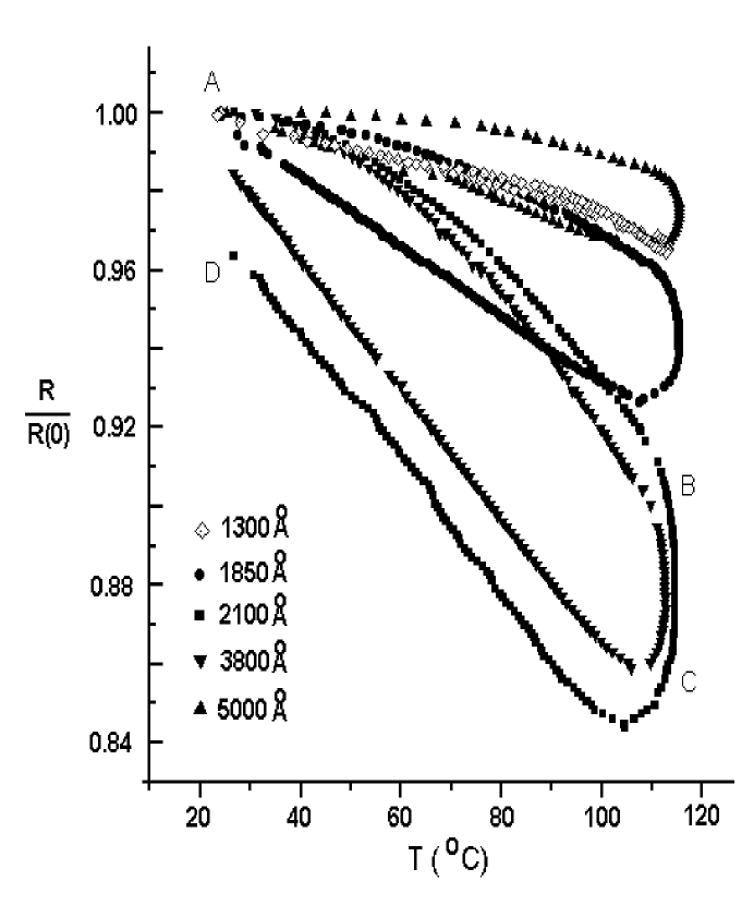
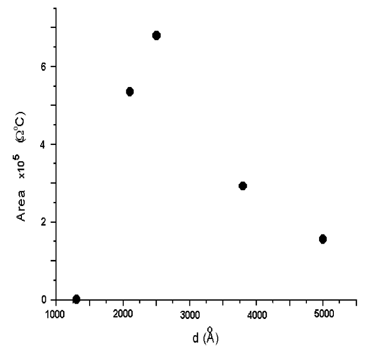
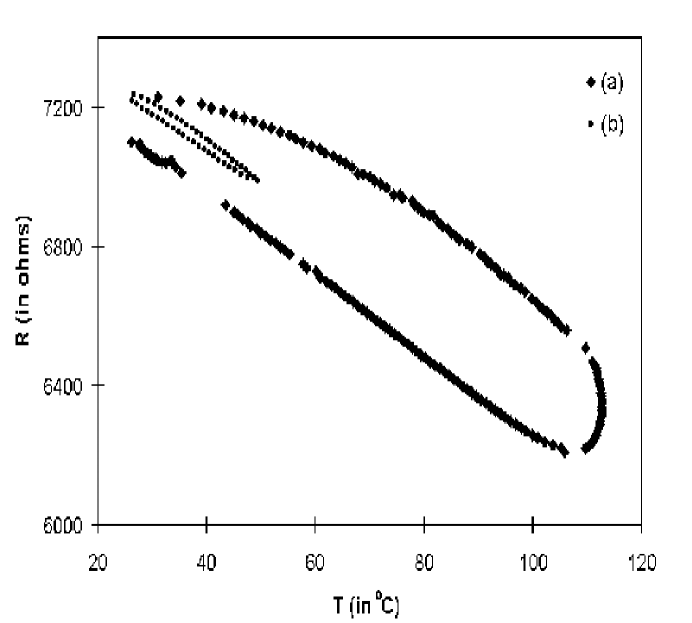
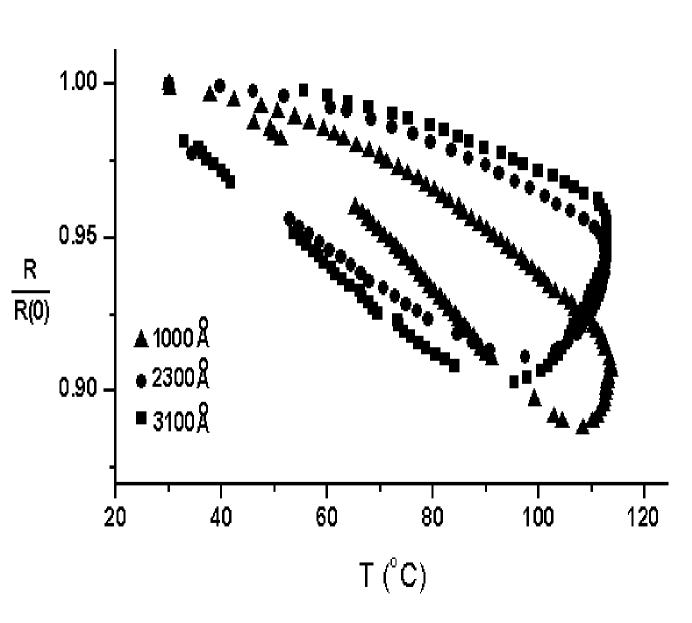
Films of different thickness were heated at the same heating rate to reach identical maximum temperature (). Figure 3 shows the hysteresis paths taken during the heating and cooling processes for various film thicknesses. We have marked three different regions as ”AB”, ”BC” and ”CD” on the hysteresis loop. The resistance decreases with increasing temperature (region ”AB”) indicating the semiconducting nature of the film, which is a p type narrow band gap material [8]. Point ”B” marks the point where the heater is switched off. Even though the heater was switched off, the temperature of the sample does not decrease immediately as the measurements were done in vacuum (see figure 1). However, the resistance continues to fall till point ”C” at the almost constant temperature within some span of time. Thus, variation in resistance in region ”BC” is with time. Hence, in figure 4, we show the variation of resistance with time. As can be seen, the heater is switched off at ’B’ and the resistance of the sample continues to decrease with time till the onset of the cooling process marked by point ”C”. It may be noted that the measured temperature in the region ’BC’ was constant as shown in figure 3 and the decrease in resistance looks to be very steep in this region. Figure 4 depicts the same fact, that is, increasing resistance with decreasing temperature in cooling process beyond ’C’ as seen in fig 3. The increase in resistance during cooling in fig 3 (between ’CD’) is almost parallel to the decrease in segment ”AB”. At point ”D”, the film reaches room temperature and the film resistance goes back to point ”A”, very slowly, over a long time ( 8-9 hours). The regions ”BC” and ”DA” are quite puzzling, where the temperature is constant and resistance is varying with time. It is evident that films of different thickness films enclose different area under the loop. Figure 5 shows the variation of the area enclosed under the loop for various thickness. The graph was plotted using the measured area enclosed by various loops of figure 3.
3.2 Dependence of final temperature & cooling rate
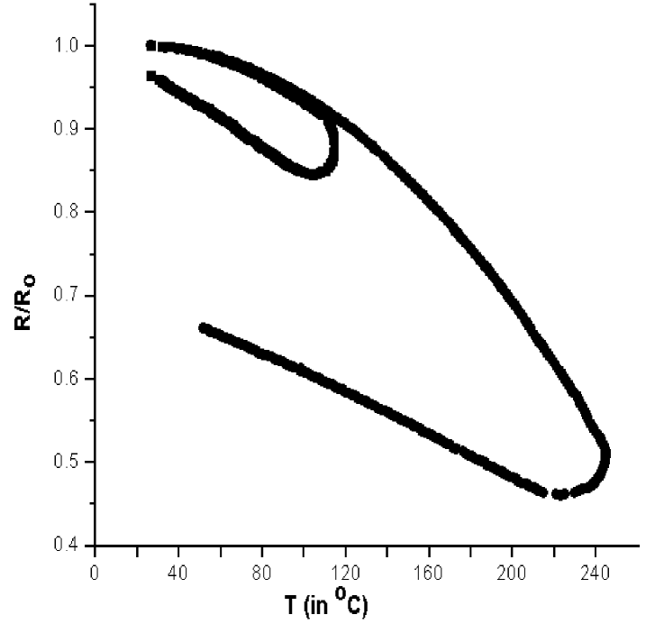
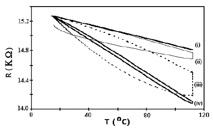
Samples of identical thickness were heated with the same heating rate but to different final temperatures by switching off the heater at different temperatures (). The segment ”AB” in such cases coincided. However, the length of the segment ”BC” varied. Figure 6 compares two cases (for clarity only two are shown) where the same film was heated at the same heating rate, but to two different . The cooling rate was not controllable in our present experiment, as it was allowed for natural cooling in vacuum. It is clear that the cooling rate strongly depends on . From the above two cases it is implied that the area under the loop is also dependent on the cooling rate of the films. The explicit dependence of cooling rate could also be studied with a convenient and controllable cooling arrangement which is not possible in the present study.
3.3 Dependence of heating rate
To understand the effect of heating rate on the area enclosed by the loop, films of same thickness were heated at different heating rates, as shown in figure 7. From equation 2, the heating rate also varies with time. It’s magnitude depends on and Q, both of which can be controlled or selected by the voltage applied to the heater. It is evident from figure 7, dR/dT is greater for lower heating rate. The slope is larger for lower rate of heating, resulting in smaller area enclosed. Hence the area enclosed increases with increasing heating rate. In other words the rate of change of resistance, or the thermal coefficient of resistance depends on the heating rate.
In summary the area under the hysteresis loop hence, was found mainly to depend
on the following parameters of the experiment:
(a) the film thickness
(b) the heating rate
(c) the final temperature () that the sample was heated to
and
(d) the rate of cooling
Most of these observations can be explained qualitatively suing the theory in [6]. However, we briefly outline the theory and the model below.
4 Theory
We first calculate the temperature profile along the film thickness which need not be uniform especially during heating/ cooling process in a dynamic or transient measurement. Then the calculation of the total resistance of the film as a function of temperature can simply be carried out by integrating across the film thickness. This should be the key in explaining the observed hysteresis behavior. As described earlier the film is kept on copper block being heated. Heating proceeds from the substrate side. Therefore, the temperature varies along the film thickness with time which is essentially a one dimensional problem of heating conduction across the film thickness. The variation of temperature with time and spatial co-ordinates is given by[9]
| (4) |
where is the thermal conductivity of the film and is the specific heat of the film. A solution of this partial differential equation depends on the initial and boundary conditions of the problem. Depending on the initial and boundary conditions solution would be different[10]. For the given experimental conditions the variation of temperature with spatial and time co-ordinates is given by [6]. The variation in temperature along the film thickness with time is given as
| (5) |
where D is the thermal diffusivity () and d is the film thickness. The temperature profile across the film thickness can be calculated using equation 7. At the starting of heating, in the equation can simply be taken as room temperature with slightly hotter by few degrees. Every time a new resulting is used along with the incremented . Thus, the profile can be calculated numerically. serves as the heat source. Obviously, the difference between and would increase with decreasing D or of the given material exhibiting a quite non-uniform temperature distribution along the film thickness at the given instant of time. The time for reaching equilibrium or uniform distribution is also inversely proportional to of the material because does not vary much from material to material at high temperatures.
The film can be thought of as a stack of numerous infinitesimal identical thin layersof same thickness. All the layers acting as resistive elements with the net resistance of the film as the resistance in parallel combination of these layers. Since the layers are identical, at room temperature all of them have equal value. However, due to the metallic/ semiconducting nature of the film, the resistance of these layers vary with temperature. For simplicity, the variation of resistance with temperature is taken linear as
| (6) |
where and are the temperature coefficient of resistance (TCR) and the resistance of the identical layers respectively. For the case , the films resistance would be given as
| (7) |
The TCR is positive for metal while it is negative for semiconductors. Since, spatial distribution of temperature along thickness was calculated for various substrate temperatures at various instant, the films resistance can be trivially calculated as a function of substrate temperature and time.
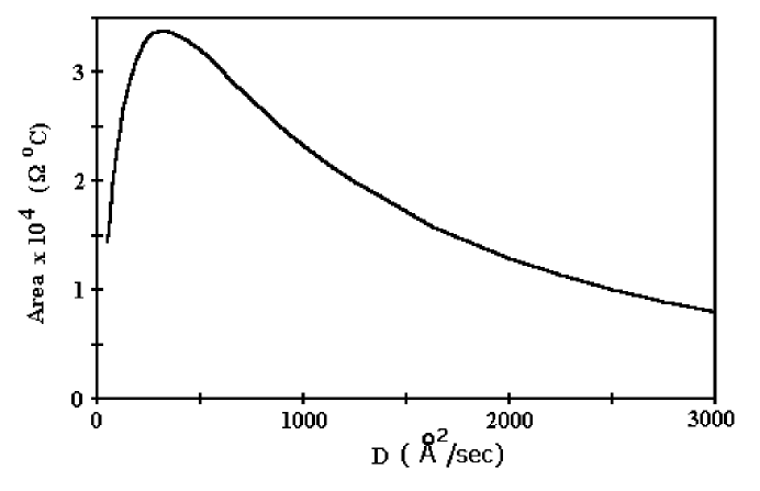
We have calculated the film resistance as a function of temperature as described above using eqn(5-7). We have taken 100nm thick film as a stack of 10 identical layers in parallel combination with each layer’s resistance of at room temperature and . These numerical values are taken from our previous study on films [11]. The results are plotted in fig 8 for varying diffusivity or mainly the thermal conductivity. The visual examination of fig 8 reveals a peaking behavior of hysteresis loop area with thermal conductivity of the film. We have, therefore, plotted the hysteresis loop area exclusively as a function of diffusivity in fig 9. The loop area shows a maximum at intermediate diffusivity. This may look very surprising on the onset. However, there is a striking similarity between fig 5 and fig 9, that is dependence of loop area on film thickness and thermal conductivity. Fig 9 is the direct consequence of varying thermal conductivity as calculated by the above model resulting from the temperature profile across the film thickness. The film resistance, the parallel combination of identical resistive layers would crucially depend on the temperature profile across the thickness. The results could be almost similar for very low thermal conductivity and very high thermal conductivity due to nearly uniform temperature profile. Therefore, an increased or enhanced loop area for moderate thermal conductivity seems to be quite reasonable arising due to quite non-uniform temperature profile across film thickness.
The similarity between the behavior of loop area with film thickness and thermal conductivity may also be expected because many physical properties like thermal conductivity show thickness dependence [12]. The exact dependence may vary from material to material. In the present study, films are semi-metallic and shows a linearly inverse relation of resistance with film thickness [11]. in the range of fig 5. Since films are semi-metallic, by Wiedemann-Franz law, we can see that thermal conductivity varies linearly with film thickness. Therefore, the experimental result of thickness dependence of loop area shows an analogous behavior to that predicted by the calculated dependence of loop area on thermal conductivity. However, the resistivity od films is slightly lower larger due to its polycrystalline nature. Still we feel it is within the applicability of Wiedemann-Franz law. Also, the thermal conductivity used in the model calculation is the total of lattice and electron contributions. Further, we have observed hysteresis loops even in the amorphous films of as shown in fig 10. Similarly, the polycrystalline InSb films also show hysteresis. The present model explains quite well qualitatively the features of the hysteresis behavior. At present we have not fitted the experimental data with the model due to thenon-availability of few material parameters required. Alternatively one can estimate thermal conductivity of the film across its thickness by fitting the experimental data and the model. It would be same along parallel and perpendicular directions of the film for isotropic materials and differ for anisotropic materials. We are pursuing few other different materials in this direction along with quantitative analysis and fitting of experimental data for the determination of thermal conductivity. However, the detailed analysis will be the subject for future publication.
5 Conclusions
The electrical studies of thin films are usually done by heating the sample and measuring resistance/ resistivity with temperature. Though, the measurements are to be done after the film has attained a steady temperature, usually the measurement is done as the film is being heated or cooled. As discussed in the article, if the film has a finite thermal conductivity, one essentially is making measurement in non-equilibrium conditions. Thus, parameters like TCR etc. computed is not only material dependent but depends on conditions of the experiment, e.g. the rate of heating or cooling. It is essentially due to this non-equilibrium measurement that leads to a loop like formation due to the heating-cooling cycle. Where the area enclosed by the loop depends on the films’ thermal conductivity, rate of heating and cooling. This method may be developed to index the film’s diffusivity.
References
- [1] V. Damodara Das and D. Karunakaran, Phys. Rev. B., 39 (1989) 10 872.
- [2] V. Damodara Das and P. Gopal Ganesan, Solid State Commun., 106 (1998) 315.
- [3] V. Damodara Das and S. Selvaraj, J. Appl. Phys., 83 (1993) 3696.
- [4] K. Jayachandran and C. S. Menon, Pramana, 50 (1998) 221.
- [5] Y. Sakamoto and I. Takashima, J. Phys.: Cond. Matt., 8, (1996), 10511.
- [6] P. Arun and A. G. Vedeshwar, Phys. Lett. A., 313 (2003), 126.
- [7] P. Arun, Pankaj Tyagi and A. G. Vedeshwar, Physica B, 307 (2001), 105.
- [8] I. Lefebvre, M. Lannoo, G. Allan, A. Ibanez, J. Fourcade, J. C. Jumas and E. Beaurepaire, Phys. Rev. Lett., 59, (1987), 2471.
- [9] H. S. Carslaw and J. C. Jaeger, ”Conduction of Heat in Solids”, (Oxford Univ. Press, Oxford 1954).
- [10] S. M. Sze, ”Semiconductor Devices, Physics and Technology”, (Wiley, New York 1993).
- [11] P. Arun and A. G. Vedeshwar, Mater. Res. Bull., 38, 1929-38 (2003).
- [12] L. I. Maissel and R. Glang, ”Handbook of thin film technology”, (Mc GrawHill, New York, 1970).

[tbh]