Influence of magnetic impurities on charge transport in diffusive-normal-metal / superconductor junctions
Abstract
Charge transport in the diffusive normal metal (DN) / insulator / - and -wave superconductor junctions is studied in the presence of magnetic impurities in DN in the framework of the quasiclassical Usadel equations with the generalized boundary conditions. The cases of - and -wave superconducting electrodes are considered. The junction conductance is calculated as a function of a bias voltage for various parameters of the DN metal: resistivity, Thouless energy, the magnetic impurity scattering rate and the transparency of the insulating barrier between DN and a superconductor. It is shown that the proximity effect is suppressed by magnetic impurity scattering in DN for any value of the barrier transparency. In low-transparent -wave junctions this leads to the suppression of the normalized zero-bias conductance. In contrast to that, in high transparent junctions zero-bias conductance is enhanced by magnetic impurity scattering. The physical origin of this effect is discussed. For the -wave junctions, the dependence on the misorientation angle between the interface normal and the crystal axis of a superconductor is studied. The zero-bias conductance peak is suppressed by the magnetic impurity scattering only for low transparent junctions with . In other cases the conductance of the -wave junctions does not depend on the magnetic impurity scattering due to strong suppression of the proximity effect by the midgap Andreev resonant states.
pacs:
PACS numbers: 74.50.+r, 74.20.-zI Introduction
Nowadays, thanks to the nanofabrication technique, detailed experimental studies of the electron coherence in mesoscopic superconducting systems become possible, where the Andreev reflection Andreev ; BTK ; Zaitsev plays an important role in the low energy transport. In diffusive normal metal / superconductor (DN/S) junctions, the phase coherence between incoming electrons and Andreev reflected holes persists in DN at a mesoscopic length scale and results in strong interference effects on the probability of Andreev reflection Hekking .
One of the remarkable experimental manifestations of the coherent Andreev reflection is the zero bias conductance peak (ZBCP) in DN/S junctions Giazotto ; Klapwijk ; Kastalsky ; Nguyen ; Wees ; Nitta ; Bakker ; Xiong ; Magnee ; Kutch ; Poirier . The physics of ZBCP was extensively studied theoretically using scattering matrix approach Beenakker1 ; Lambert ; Takane ; Beenakker2 ; reflec ; Lesovik and the quasiclassical Green’s function technique Volkov ; Nazarov1 ; Yip ; Yip2 ; Stoof ; Reentrance ; Golubov ; Takayanagi ; Bezuglyi ; Seviour ; Belzig . Volkov, Zaitsev and Klapwijk (VZK) Volkov explained the origin of the ZBCP in DN/S junctions in the framework of the quasiclassical theory by solving the Usadel equations Usadel with the Kupriyanov and Lukichev (KL) boundary condition for the Keldysh-Nambu Green’s function KL . According to the VZK theory the ZBCP is due to the enhancement of the pair amplitude in DN by the proximity effect. The influence of the magnetic impurity scattering on the bias voltage dependent conductance was also studied within this approach Volkov ; Yip2 ; Belzig1 .
Recently the VZK theory for -wave superconductors was extended by Tanaka et al. TGK using more general boundary conditions provided by the circuit theory of Nazarov Nazarov2 . These boundary conditions treat an interface as an arbitrary connector between diffusive metals. The connector is characterized by a set of transmission coefficients ranging from a ballistic point contact to a tunnel junction. The boundary conditions coincide with the KL conditions when a connector is diffusive or transmission coefficients are low, while the BTK theory BTK is reproduced in the ballistic regime. The extended VZK theory TGK ; PRB2004 revealed a number of new features like a -shaped gap like structure and a crossover from a zero bias conductance peak (ZBCP) to a zero bias conductance dip (ZBCD). These phenomena are relevant for the actual junctions in which the barrier transparency is not necessarily small. However, the influence of the magnetic impurity scattering in DN on the charge transport was not studied in this regime.
The generalized VZK theory was recently applied also to unconventional superconducting junctions Nazarov3 ; PRB2004 . The formation of the midgap Andreev resonant states (MARS) at the interface of unconventional superconductors Buch ; TK95 ; Kashi00 ; Experiments is naturally taken into account in this approach Nazarov3 ; PRB2004 . It was demonstrated that the formation of MARS in DN/-wave superconductor(DN/) junctions strongly competes with the proximity effect. Remarkable recent advances in experiments on tunneling in high cuprates Hiromi stimulate an interest to the problem of an influence of the magnetic impurity scattering on a charge transport in DN/ junctions.
In the present paper the generalized VZK theory is applied to the study of an influence of the magnetic impurity scattering in the DN on the conductance in DN/S where S is either - or -wave superconductor. The parameters of the problem are the height of the insulating barrier at the DN/S interface, the resistance , the magnetic impurity scattering rate , the Thouless energy in DN and the angle between the normal to the interface and the crystal axis of -wave superconductors. We shall focus on the dependence of the normalized conductance , on the bias voltage , where are the conductances in the superconducting (normal ) state. The organization of the paper is as follows. In section II the detailed derivation of the expression for the normalized conductance is provided. In sections III the results of calculations of are presented for - and -wave junctions separately and physical explanation of the results is given. In section IV the summary of the obtained results and the conclusions are presented. In this paper we restrict ourselves to the low-temperature regime and put .
II Formulation
In this section we introduce the model and the formalism. We consider a junction consisting of normal and superconducting reservoirs connected by a quasi-one-dimensional diffusive conductor (DN) with a length much larger than the mean free path. This structure was considered in Ref. TGK ; PRB2004 , while in the present paper the scattering on magnetic impurities in DN is taken into account. Similar to Ref. TGK ; PRB2004 , we assume that the interface between the DN conductor and the S electrode at has a resistance while the DN/N interface at has zero resistance and we apply the generalized boundary conditions of Ref. Nazarov2 to treat the interface between DN and S.
We model the insulating barrier between DN and S by the delta function , which provides the transparency of the junction , where is a dimensionless constant, is the injection angle measured from the interface normal to the junction and is Fermi velocity. The interface resistance is given by
where is Sharvin resistance , is the Fermi wave-vector and is the constriction area (see Fig. 1). Note that the area is in general not equal to the cross-section area of the normal conductor, therefore is independent parameter of our theory. This allows to vary independently of . In real physical situation, the assumption means that only a part of the actual flat DN/S interface (having area ) is conducting, no matter is it a single conducting region or a series of such regions. These conducting regions are not constrictions in a standard sense - we don’t assume the narrowing of the total cross-section, but rather that only the part of the cross-section is conducting.
We apply the quasiclassical Keldysh formalism in the following calculation of the conductance. The definitions of 4 4 Green’s functions in DN and S, and , and other notations can be found in Ref. TGK ; PRB2004 . The new feature in the present model is the spin-scattering term in the static Usadel equation Usadel for in DN
| (1) |
where is the diffusion constant in DN, is given by
with , and
is the self-energy for magnetic impurity scattering with the scattering rate in DN. Note that magnetic impurities take random alignments and we average them in all directions, thus in our calculation is a unit matrix in the spin space. The Nazarov’s generalized boundary condition for at the DN/S interface has the same form as the one without magnetic impurity scattering (see Ref. TGK ; PRB2004 ).

In the actual calculation it is convenient to use the standard -parametrization where is a measure of the proximity effect in DN and is determined by the following equation
| (2) |
One can see that introduction of magnetic impurity scattering leads to modification of the effective coherence length in DN. In particular, switching on makes function exponentially decaying at zero energy, while at behaves linearly in DN. It will be shown below that these modifications result in suppression of in DN, as expected due to pair-breaking nature of magnetic scattering, which in turn leads to corresponding modifications of the subgap conductance.
Finally, we obtain the following result for the electric current
| (3) |
Then the total resistance for -wave junction at zero temperature is given by
| (4) |
with
| (5) |
| (6) |
For a -wave junction, the function is given by the following expression
, and . In the above , and denote the angle between the normal to the interface and the crystal axis of -wave superconductors, the imaginary part of and respectively. The conductance in the superconducting state is simply related to by .
It is important to note that in the present approach, according to the circuit theory, can be varied independently of , , independently of , since one can change the magnitude of the constriction area independently. In other words, is no more proportional to , where is the averaged transmissivity of the barrier and is the mean free path in the diffusive region. Based on this fact, we can choose and as independent parameters.
In the following section, we will discuss the normalized conductance where is the conductance in the normal state without magnetic impurity given by .
III Results
III.1 Tunneling conductance for -wave junctions
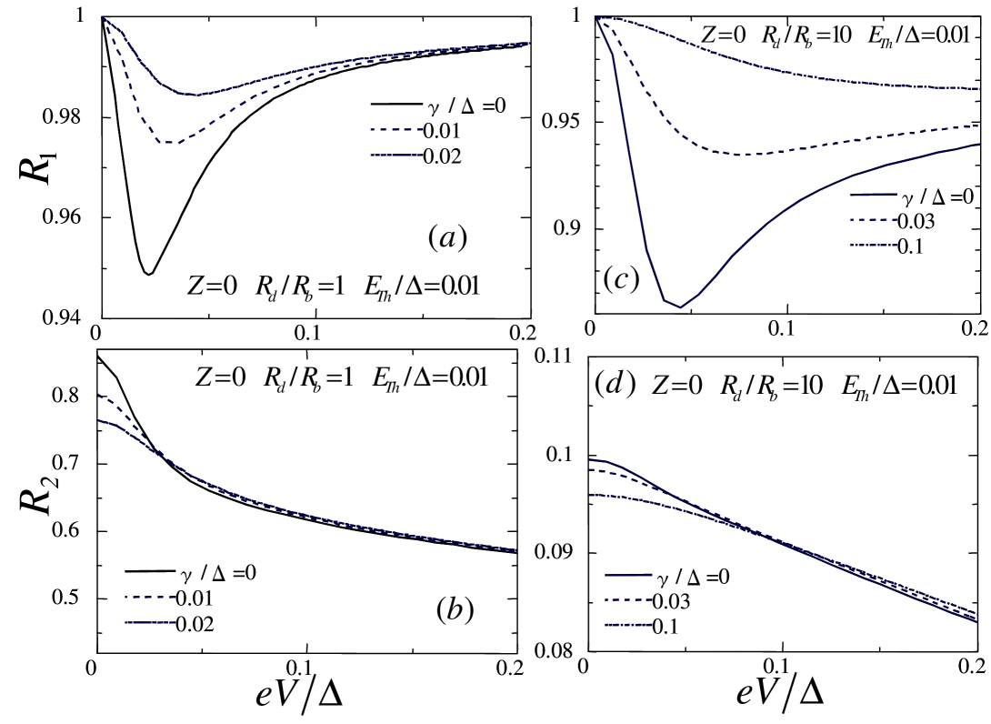
In this section, we focus on the bias voltage dependent normalized conductance for various situations. Let us first focus on the relatively low transparent junctions with for various (Fig. 2). For and , the curves have a rounded bottom shape and the height of the bottom value is reduced with an increase in . The height of the peak at is reduced with an increase in (see Fig. 2(a)). For and , the curves also have a rounded bottom structure which flattens with an increase in . Also the peak at is suppressed with the increase of (see Fig. 2(b)). For small Thouless energy and , the conductance has a prominent ZBCP with the width given by . As seen from Fig. 2(c), the magnetic impurity scattering suppresses the peak height. With the increase of the resistance ratio , the ZBCP transforms into ZBCD, as shown in Fig. 2(d). The magnitude of ZBCD decreases with the increase of , and the height of the peaks around is also reduced (see Fig. 2 (d)). As seen from these figures, the characteristic energy range of which modifies the magnitude of , is determined by , in agreement with the previous study based on the KL boundary conditions Yip2 .
In the case of an intermediate barrier strength (Fig. 3) the magnitude of always exceeds unity. The resulting line shapes of for are quite similar to the corresponding curves for (see Figs. 3(a) and 3(b)). For and , the zero-bias value is independent of (see Fig 3(a)), in contrast to the corresponding case shown in Fig. 2(a). Another important difference from the case of large -factor is the absence of ZBCP for low Thouless energy. It is seen that for a ZBCD occurs in both cases of and . This conductance dip and the finite voltage peaks are fully suppressed with the increase of for (see Fig. 3(c)). On the other hand, for only the peaks around are suppressed while the magnitude of does not depend on , similar to the case (see Fig. 3(d)). The relevant scale of is again given by the magnitude of .
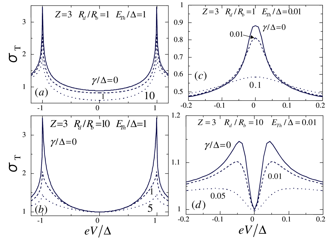
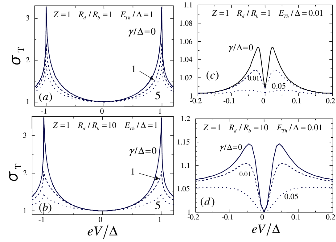
For fully transparent case with (Fig. 4), also always exceeds unity. The line shapes of with are similar to the corresponding curves for and (see Figs. 4(a) and 4(b)). For and , the magnitude of is enhanced by in contrast to the corresponding cases shown in Figs. 2(a) and 3(a)(see Fig 4(a)). For and , have a ZBCD. The magnitude of is enhanced by and the depth of the ZBCD decreases with the increase of (see Fig. 4(c)). On the other hand, for and , the magnitude of does not depend on while the finite bias peaks are suppressed similar to the cases of and (see Fig. 4(d)).

In order to understand the above wide variety of line shapes and their relation to the proximity effect, we shall discuss the behavior of function which is the measure of the proximity effect at the DN/S interface and determines the normalized local density of states by . At is always a real number even for non zero . First, we study the case of and (Fig. 5) where the same values of and are chosen as in Fig. 2. The real part of has a step function like structure and it is always positive for and negative otherwise. The absolute value of the real part of decreases with an increase in . At the same time, the imaginary part of has a coherent peak, the height of which is reduced with an increase in . For the case of and (Fig. 6) where the same values of are chosen as in Fig. 2, the real part of has a ZBCP with the width given by . The imaginary part of has a ZBCD for . Both the amplitudes of the real and imaginary part of are reduced with the increase of only around zero energy in the interval of the order of .
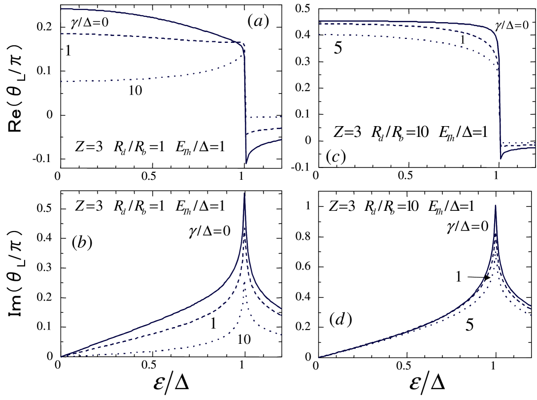
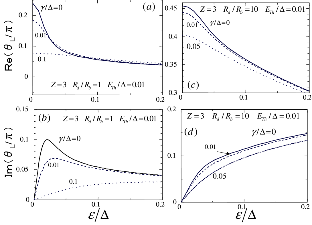
Next we consider the case of with (Fig. 7) and (Fig. 8) where the same values of are chosen as in Fig. 4. The line shapes of both and are similar to those in Figs. 5 and 6. There is no clear qualitative difference between the energy dependencies of for and those for . For all cases, the magnitude of is reduced with the increase of and then the proximity effect is suppressed by the magnetic impurity scattering within the energy range determined by . In almost all cases, the magnitude of is reduced with the decrease of . Only for high transparent case with not so large , the decrease of the magnitude of , , the reduction of the proximity effect, can enhance the magnitude of .


In the following, we explain the wide variety of the line shapes of . We consider and case, where has a weak energy dependence around zero voltage. For the fully transparent case with , i.e., , can be given by
| (7) |
with
| (8) |
From this equation we find that the magnitude of gets close to unity under the strong proximity effect, i.e., when the magnitude of is large. As shown in Figs. 7(a) and 7(b), the magnitude of at is lowered with an increase in for . Then , according to Eqs. (7) and (8), the resulting around is slightly enhanced as shown in Fig. 4(a). For , the magnitude of is much larger than the magnitude of . Then the dependence of becomes negligible as shown in Fig. 4(b). In order to understand the case of and the small magnitude of , we decompose into and following the previous workTGK , where and are defined by
and
Fig. 9 shows that has a minimum at a finite voltage which can result in a ZBCD and that has a maximum for high transparent junctions. For a large magnitude of , the effect of is dominant, then the normalized conductance always has a ZBCD (see Figs. 9(c), 9(d) and 4(d)). Since has a maximum at zero voltage (Fig. 9(b)), the resulting has a ZBCD as shown in Fig. 4(c).
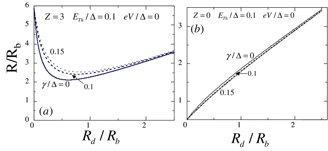
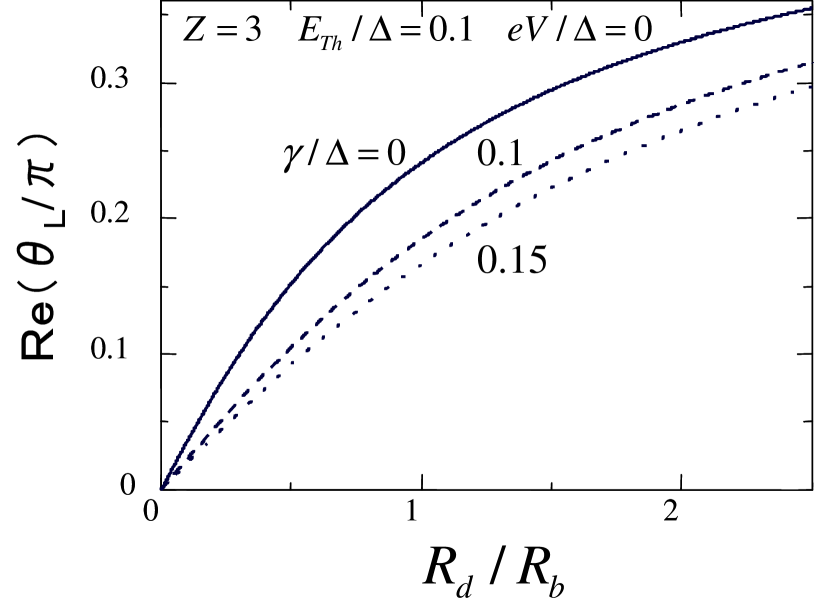
Next we focus on the zero voltage resistance as a function of . For , has a reentrant behavior as a function of due to the so called reflectionless tunneling effect reflec (see Fig. 10(a)). With the increase of , this effect is smeared since the magnitude of is reduced as shown in Fig. 11. In contrast, for , where increases monotonically as a function of , the dependence of is very weak (see Fig. 10(b)).
III.2 Tunneling conductance for -wave junctions
Below we discuss the results of calculations for the -wave case. Fig. 12 shows the normalized conductance for , , , and where denotes the the misorientation angle between the normal to the interface and the crystal axis of -wave superconductors. In this case, MARS are not formed at the interface of the -wave superconductor. The origin of the ZBCP is due to the proximity effect in the DN region and the height of the ZBCP is suppressed with increasing similar to the case of the -wave junctions.
With the increase of the magnitude of the MARS are formed at the interface. The MARS contribute to the charge transport across the junction and leads to the formation of the ZBCP. As is seen in Fig. 13, the ZBCP does not depend on for , , and . The similar result is obtained for different angle . The reason is that MARS reduce the proximity effect in DN, therefore the influence of magnetic impurity scattering on the becomes less important. In the extreme case, , the proximity effect is completely absent by the symmetry of the pair potential and is completely independent of .
IV Conclusions
We have performed a detailed theoretical study of the conductance of diffusive normal metal / - and -wave superconductor junctions in the presence of magnetic impurities. Below the main results obtained in this paper are summarized.
1. For the -wave junctions, the proximity effect is suppressed by the magnetic impurity scattering within the energy range determined by the Thouless energy in DN. In this range both the real and imaginary parts of the proximity effect parameter, i.e., and are reduced with the increase of the magnitude of for any transparency of the insulating barrier.
2. The magnitude of the normalized bias voltage dependent conductance in the low transparent -wave junctions is suppressed by the magnetic impurity scattering. On the other hand, for high transparent -wave junctions, can be enhanced by the magnetic impurity scattering.
3. In the -wave junctions, the zero bias conductance peak formed for low transparent barriers is suppressed by the magnetic impurity scattering only for . For other misorientation angles the conductance is not sensitive to the magnetic impurity scattering in a diffusive normal metal.
In the present paper, we have discussed the case where magnetic impurities are located in DN. These results can be also applied to the situation when the junction is in a weak magnetic field . If the field direction is parallel to the junction plane, the pair-breaking rate is given by , where is the transverse size of the DNBelzig1 . Assuming , , , and , we estimate the pair-breaking rate . This range of corresponds to the parameters chosen in the present paper. The suppression of the ZBCP and ZBCD by the magnetic field was actually observed in several experimentsGiazotto ; Kastalsky ; Bakker ; Xiong ; Magnee ; Poirier . The results of the present paper may serve as a guide to study the charge transport in the junctions with magnetic impurities or under applied magnetic field.
It is also an interesting problem to study the influence of the magnetic impurity scattering on diffusive normal metal / triplet superconductor junctions where anomalous proximity effect is expected pwave . An application of the present theory to the S/N/S junctions with unconventional superconductors also requires separate investigation.
The authors appreciate useful and fruitful discussions with Yu. Nazarov and H. Itoh. This work was supported by the Core Research for Evolutional Science and Technology (CREST) of the Japan Science and Technology Corporation (JST) and a Grant-in-Aid for the 21st Century COE ”Frontiers of Computational Science”. The computational aspect of this work has been performed at the facilities of the Supercomputer Center, Institute for Solid State Physics, University of Tokyo and the Computer Center.
References
- (1) A.F. Andreev, Sov. Phys. JETP 19, 1228 (1964).
- (2) G.E. Blonder, M. Tinkham, and T.M. Klapwijk, Phys. Rev. B 25, 4515 (1982).
- (3) A. V. Zaitsev, Sov. Phys. JETP 59, 1163 (1984).
- (4) F. W. J. Hekking and Yu. V. Nazarov, Phys. Rev. Lett. 71, 1625 (1993).
- (5) F. Giazotto, P. Pingue, F. Beltram, M. Lazzarino, D. Orani, S. Rubini, and A. Franciosi, Phys. Rev. Lett. 87, 216808 (2001).
- (6) T.M. Klapwijk, Physica B 197, 481 (1994).
- (7) A. Kastalsky, A.W. Kleinsasser, L.H. Greene, R. Bhat, F.P. Milliken, J.P. Harbison, Phys. Rev. Lett. 67, 3026 (1991).
- (8) C. Nguyen, H. Kroemer and E.L. Hu, Phys. Rev. Lett. 69, 2847 (1992).
- (9) B.J. van Wees, P. de Vries, P. Magnee, and T.M. Klapwijk, Phys. Rev. Lett. 69, 510 (1992).
- (10) J. Nitta, T. Akazaki and H. Takayanagi, Phys. Rev. B 49 3659 (1994).
- (11) S.J.M. Bakker, E. van der Drift, T.M. Klapwijk, H.M. Jaeger, and S. Radelaar, Phys. Rev. B 49, 13275 (1994).
- (12) P. Xiong, G. Xiao and R.B. Laibowitz, Phys. Rev. Lett. 71, 1907 (1993).
- (13) P.H.C. Magnee, N. van der Post, P.H.M. Kooistra, B.J. van Wees, and T.M. Klapwijk, Phys. Rev. B 50, 4594 (1994).
- (14) J. Kutchinsky, R. Taboryski, T. Clausen, C. B. Sorensen, A. Kristensen, P. E. Lindelof, J. Bindslev Hansen, C. Schelde Jacobsen, and J. L. Skov, Phys.Rev. Lett. 78 ,931 (1997).
- (15) W. Poirier, D. Mailly, and M. Sanquer, Phys. Rev. Lett. 79, 2105 (1997).
- (16) C.W.J. Beenakker, Rev. Mod. Phys. 69, 731 (1997);
- (17) C.J. Lambert, J. Phys. Condens. Matter 3, 6579 (1991);
- (18) Y. Takane and H. Ebisawa, J. Phys. Soc. Jpn. 61, 2858 (1992).
- (19) C.W.J. Beenakker, Phys. Rev. B 46, 12841 (1992).
- (20) C. W. J. Beenakker, B. Rejaei, and J. A. Melsen, Phys. Rev. Lett. 72, 2470 (1994).
- (21) G.B. Lesovik, A.L. Fauchere, and G. Blatter, Phys. Rev. B 55, 3146 (1997).
- (22) A.F. Volkov, A.V. Zaitsev and T.M. Klapwijk, Physica C 210, 21 (1993).
- (23) K.D. Usadel Phys. Rev. Lett. 25, 507 (1970).
- (24) M.Yu. Kupriyanov and V. F. Lukichev, Zh. Exp. Teor. Fiz. 94 (1988) 139 [Sov. Phys. JETP 67, (1988) 1163].
- (25) Yu. V. Nazarov, Phys. Rev. Lett. 73, 1420 (1994).
- (26) S. Yip, Phys. Rev. B 52, 3087 (1995).
- (27) S. Yip, Phys. Rev. B 52, 15504 (1995).
- (28) Yu. V. Nazarov and T. H. Stoof, Phys. Rev. Lett. 76, 823 (1996); T. H. Stoof and Yu. V. Nazarov, Phys. Rev. B 53, 14496 (1996).
- (29) A. F. Volkov, N. Allsopp, and C. J. Lambert, J. Phys. Cond. Mat. 8, L45 (1996); A. F. Volkov and H. Takayanagi, Phys. Rev. B 56, 11184 (1997).
- (30) A.A. Golubov, F.K. Wilhelm, and A.D. Zaikin, Phys. Rev. B 55, 1123 (1997).
- (31) A.F. Volkov and H. Takayanagi, Phys. Rev. B 56, 11184 (1997).
- (32) E. V. Bezuglyi, E. N. Bratus’, V. S. Shumeiko, G. Wendin and H. Takayanagi, Phys. Rev. B 62, 14439 (2000).
- (33) R. Seviour and A. F. Volkov, Phys. Rev. B 61, R9273 (2000).
- (34) W. Belzig, F. K. Wilhelm, C. Bruder, et al., Superlattices and Microstructures 25, 1251 (1999).
- (35) W. Belzig, C. Bruder, and G. Schön, Phys. Rev. B 54 9443 (1996).
- (36) Yu. V. Nazarov, Superlattices and Microstructuctures 25, 1221 (1999), cond-mat/9811155.
- (37) Y. Tanaka, A. A. Golubov and S. Kashiwaya, Phys. Rev. B 68 054513 (2003).
- (38) L.J. Buchholtz and G. Zwicknagl, Phys. Rev. B 23 5788 (1981); C. Bruder, Phys. Rev. B 41, 4017 (1990); C.R. Hu, Phys. Rev. Lett. 72, 1526 (1994).
- (39) Y. Tanaka and S. Kashiwaya, Phys. Rev. Lett. 74, 3451 (1995); S. Kashiwaya, Y. Tanaka, M. Koyanagi and K. Kajimura, Phys. Rev. B 53, 2667 (1996); Y. Tanuma, Y. Tanaka, and S. Kashiwaya Phys. Rev. B 64, 214519 (2001), Y. Asano , Y. Tanaka and S. Kashiwaya, Phys. Rev. B 69, 134501 (2004).
- (40) S. Kashiwaya and Y. Tanaka, Rep. Prog. Phys. 63, 1641 (2000) and references therein.
- (41) J. Geerk, X.X. Xi, and G. Linker: Z. Phys. B. 73,(1988) 329; S. Kashiwaya, Y. Tanaka, M. Koyanagi, H. Takashima, and K. Kajimura, Phys. Rev. B 51 1350 (1995); L. Alff, H. Takashima, S. Kashiwaya, N. Terada, H. Ihara, Y. Tanaka, M. Koyanagi, and K. Kajimura, Phys. Rev. B 55, 14757 (1997); M. Covington, M. Aprili, E. Paraoanu, L.H. Greene, F. Xu, J. Zhu, and C.A. Mirkin, Phys. Rev. Lett. 79, 277 (1997); J. Y. T. Wei, N.-C. Yeh, D. F. Garrigus and M. Strasik: Phys. Rev. Lett. 81, (1998) 2542; I. Iguchi, W. Wang, M. Yamazaki, Y. Tanaka, and S. Kashiwaya: Phys. Rev. B 62, (2000) R6131; F. Laube, G. Goll, H.v. Löhneysen, M. Fogelström, and F. Lichtenberg, Phys. Rev. Lett. 84, 1595 (2000); Z.Q. Mao, K.D. Nelson, R. Jin, Y. Liu, and Y. Maeno, Phys. Rev. Lett. 87, 037003 (2001); Ch. Wälti, H.R. Ott, Z. Fisk, and J.L. Smith, Phys. Rev. Lett. 84, 5616 (2000); H. Aubin, L. H. Greene, Sha Jian and D. G. Hinks, Phys. Rev. Lett. 89, 177001 (2002); Z. Q. Mao, M. M. Rosario, K. D. Nelson, K. Wu, I. G. Deac, P. Schiffer, Y. Liu, T. He, K. A. Regan, and R. J. Cava Phys. Rev. B 67, 094502 (2003); A. Sharoni, O. Millo, A. Kohen, Y. Dagan, R. Beck, G. Deutscher, and G. Koren Phys. Rev. B 65, 134526 (2002); A. Kohen, G. Leibovitch, and G. Deutscher Phys. Rev. Lett. 90, 207005 (2003); H. Kashiwaya, A.Sawa, S. Kashiwaya, H. Yamasaki, M. Koyanagi, I. Kurosawa, Y. Tanaka and I. Iguchi Physica C, 357-360 1610 (2001).
- (42) H. Kashiwaya, I. Kurosawa, S. Kashiwaya, A. Sawa and Y. Tanaka, Phys. Rev. B 68 054527 (2003); H. Kashiwaya, S. Kashiwaya, B. Prijamboedi, A. Sawa, I. Kurosawa, Y. Tanaka, and I. Iguchi, Phys. Rev. B 70, 094501 (2004).
- (43) Y. Tanaka, Y.V. Nazarov and S. Kashiwaya, Phys. Rev. Lett. 90 167003 (2003).
- (44) Y. Tanaka, Y. V.Nazarov , A.A. Golubov and S. Kashiwaya, Phys Rev. B 69 144519 (2004).
- (45) Y. Tanaka and S. Kashiwaya, Phys. Rev. B 69 012507 (2004).