Observation of single defect relaxation in a freely suspended nano resonator
Abstract
Relaxation of single defects in a nanometer sized resonator is observed by coupling surface acoustic waves to a freely suspended beam. The surface waves act on the resonator as driving forces being able to modify the internal friction in the beam. In analogy to classical experiments on internal friction in macroscopic samples, we perform frequency, amplitude, and temperature dependent experiments on the nano resonator and find a scenario which is consistent with the observation of single defect relaxation.
pacs:
85.85.+j, 43.35.+d, 61.72.HhThe motion of dislocations in elastic solids under periodic load is known to contribute to losses occurring in internal friction experiments Fantozzi:1 . Therefore, internal friction experiments offer a method to explore the dynamics of dislocations. This is in particular interesting if the elastic body under investigation is very small, not much larger than the typical dimension of the dislocation itself. The profound knowledge of the dominating energy dissipation mechanisms in nanometer sized resonators is in particular important in view of the visions using such systems as narrow band high frequency filters Nguyen:1 or for future sensor applications Cleland:1 . To date, mechanical resonance frequencies of nanometer sized resonators up to 1 GHz have been reported Roukes:1 . Unfortunately the dramatic reduction in resonator size over the last few years turned out to be accompanied by two undesirable facts. While nano crystalline materials seem to supply superior mechanical properties, like increased yield stresses in fine grained metals described by the Hall-Petch relationship Wang:1 , the quality factors of nano crystals under resonant excitation considerably decrease with size. For these reasons, it would be highly desirable to study the internal losses of a nano resonator under conditions where defect relaxation becomes observable.
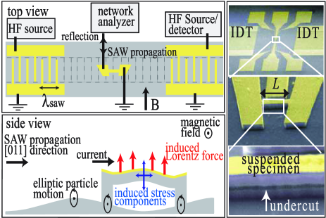
Here, we present experiments where surface acoustic waves (SAW) are used for the mechanical excitation of nano crystals. By directly probing the resonance frequency and the quality factor of a nano resonator, we are able to investigate the influence of SAW induced strain on the internal friction behavior of single defects in such a small mechanical system. Following the routes of classical experiments the strain dependent internal friction (ADIF) together with its typical temperature dependence indicate the prominent energy dissipation mechanism being mediated by line defects. Due to the small size of our nano resonator, we observe a non-classical step like increase of the damping in the ADIF experiments, which is attributed to single defects. Surface acoustic waves are perfectly suited to provide an excitation mechanism for probing attenuation effects in mechanical nano structures. SAW are acoustic modes propagating at the surface of an elastic solid, having wavelengths in the range of some microns and penetration depths of the same order. Excitation of SAW at a specific frequency is in particular effective employing a piezoelectric substrate (GaAs in our case) and properly designed interdigitated transducers (IDTs) Datta:1 . Then, a coherent acoustic ultrasonic beam is generated at the IDT’s resonance frequency . Here, km s-1 denotes the SAW velocity and the acoustic wavelength, being lithographically defined by the spacing between the fingers of the IDTs (cf. Fig. 1). As typical SAW amplitudes can range in the order of some 10 Å, they effectively modulate the acoustic properties of nano mechanical devices Beil:1 . The freely suspended nano crystals are prepared by several successive steps of electron beam lithography, anisotropic reactive ion etching (RIE), and selective isotropic wet etching. The details on production of nano mechanical devices is described in the literature Scheible:1 .
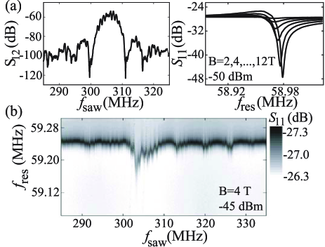
On the right of Fig. 1, we depict a top view of the setup together with an electron beam micrograph of the sample’s geometry. In our experiments, we first probe the quality factor of the resonator by standard magnetomotive excitation at the expected eigenfrequency. Here, an alternating current of the appropriate frequency is passed through the metallic top layer of the beam. The sample is placed in a strong dc magnetic field which induces a periodic Lorentz force acting on the beam. Its response is detected via standard impedance spectroscopy, and the quality factor of the resonance is determined by the relation where is the center frequency of the resonance and denotes the full width at half maximum. For low internal friction this procedure is justified, as can be shown by fitting to an appropriate equivalent circuit Beil:2 . The interaction between the nano resonator and the SAW travelling underneath it (cf. Fig. 1) is probed by measuring the changes of the magnetomotively induced signal. The SAW in this case is excited at a considerably higher frequency MHz than the beam, excluding cross talk of the IDTs to the resonator setup [cf. Fig. 2(a), left]. The response of the nano beam to magnetomotive excitation at 59 MHz is shown in Fig. 2(a, right) for different magnetic fields. As an indication for the interaction between the beam and the SAW, we observe a considerable shift of the nano mechanical resonance frequency, a decreased quality factor, and a strong attenuation of the resonance. This can be seen from Fig. 2(b), where we plot the resonator’s driving frequency versus the driving SAW frequency and code the depth of the resonance in a gray scale plot. In Fig. 3(a) the SAW-attenuation of the resonance and variation of the eigenfrequency on applied SAW power are shown. To ensure the SAW induced mechanical origin of the detuning of the beam resonance, any spurious effects have to be excluded: Pure heating of the crystal by the SAW can be shown to be a small effect Beil:1 ; Wixforth:1 . A SAW induced increase of clamping losses would be accompanied by a a larger shift in the beam’s eigenfrequency, due to a change in the form of the beam’s eigenmode. Induced currents or coupling of piezoelectric fields can also be discarded, since again they are generated at MHz, whereas the signal is detected at the beam’s eigenfrequency. Hence, the modulation of the resonator frequency and of the internal dissipation processes are attributed to a SAW mediated deformation of the oscillating beam. The responsible SAW induced strain in the nano crystal can be calculated by solving the free beam equation for the transversal amplitude of motion, taking into account time dependent boundary conditions, representing a SAW induced motion of the clamping points (cf. Fig. 1, lower left). For an elliptically polarized SAW of the Rayleigh type, the clamping points exhibit an elliptic motion in the sagittal plane, which can be expressed by the displacement vector
where , and denote the longitudinal and transversal components of the SAW propagating in the direction with frequency and wave vector component . The -axis is defined along the [011] direction, whereas the -axis is perpendicular to the sample surface. Solving the beam equation, we obtain the following expression for the SAW induced periodic strain in the beam extending from 0 to along the -axis:
where is the length of the beam. The corresponding SAW amplitude can be calculated in terms of the SAW power and the IDT geometry by
where , and are the appropriate components of the mechanical and electrical compliance tensor, respectively. is the aperture of the IDT, is the injected acoustic power of the SAW, and are constants connecting the SAW power with the induced piezoelectric fields Datta:1 . An estimated SAW amplitude of 10 Å hence induces a strain of order , resulting in a stress of N m-2. The shear strain induced by magnetomotive resonant excitation is on the order of for an amplitude of 10 Å, whereas the longitudinal strain in this case is even smaller.
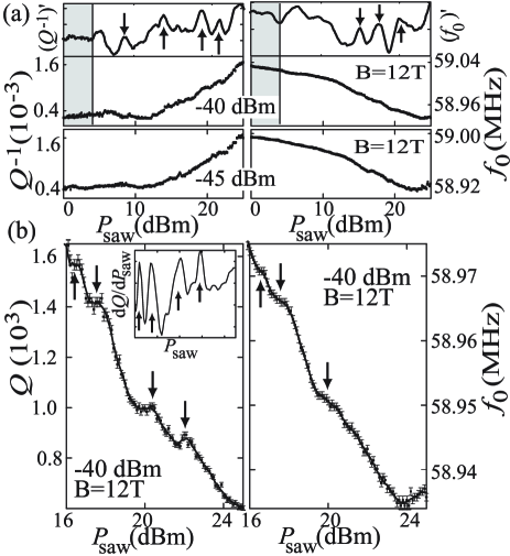
The SAW induced damping, as shown in Fig. 3(a), increases for increasing SAW amplitude about an order of magnitude. In parallel, we observe a shift of the beam’s resonance frequency to lower values. Magnifying one the characteristic traces of Fig. 3(a) reveals an interesting detail: the dramatic reduction of the resonance quality factor is accompanied by a step like decrease of the resonance frequency and quality factor [see Fig. 3(b)]. As will be confirmed by temperature dependent measurements below, we attribute the main contribution to the SAW-induced damping to the polycrystalline Au layer on top of the GaAs beam Pohl:1 . To explain the dependence of the damping on the SAW induced strain, we follow a classical string model, developed by Granato and Lücke Nowick:1 . This theory treats dislocations as vibrating strings, which execute damped oscillations under the action of a periodically applied force. A straight elastic string is pinned at both ends, the resonant frequencies of the string are calculated, and the losses associated are summed to yield a final expression for the total loss. Dislocations which are pinned to defects are treated as a series of loops becoming gradually unpinned, and increasing the length of the strings each time the net force at a pinning site overcomes a certain binding force. In this Granato-Lücke model the damping increases as , where is the dislocation loop length. For a random distribution of the pinning sites along the dislocation, Granato and Lücke obtain the following expression for the dependence of internal friction on tensile strain :
Here, and . is the dislocation density, the average loop length, and is the length of the dislocation. The theory also predicts an amplitude dependent modulus defect of the same form as Eq. (1). This theoretical description can be tested against experiments when plotting log() versus the reciprocal strain and looking for a linear dependence. The slope then varies inversely with the average loop length while the intersection with is sensitive to . These so called ’Granato-Lücke plots’ are shown in Fig.4(a) for two different ac driving powers at the beam. As expected, we obtain a linear behavior, although the occurring step-like modulations indicate a significant deviation from the classical model. To clarify this point, we note that the above string model assumes a statistical distribution of pinning centers and loop lengths. This can only be true for a large number of dislocations, which is certainly not the case for our nano beam. Moreover, the elastic energy stored in the oscillating nano crystal at the highest amplitude is of the order of 2 J 1 eV. This implies, that single defects with activation energies as low as 0.1 eV should be observable in the -value of the nano crystal resonance. In these terms, we attribute the steps in the ADIF measurements [Fig. 3(b)] to unpinning events for single dislocations in the gold layer having different activation energies. These steps in the Granato-Lücke plots tend to disappear for samples that have considerable more defects and pinning centers. Figure 4 additionally shows data obtained for another sample at 17 MHz with same dimensions, but increased thickness of the gold layer. The linear quality factor of this second sample was considerable smaller than the equivalent quantity of the first sample . This fact, together with the slope in the Granato-Lücke plot, shows that in the second sample more dislocations, with smaller average loop length, i.e. considerable more pinning centers, are present. The Granato-Lücke plots for this measurements don’t show a step like structure, due to a better statistical distribution of point defects along the dislocations.
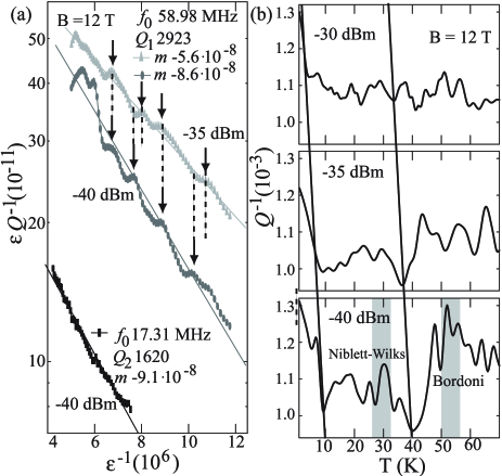
In addition to ADIF, dislocation mediated damping exhibits a characteristic temperature dependence. For macroscopic samples of fcc metals, typical traces exhibit a broad damping maximum around 120 K, known as the ’Bordoni peak’, followed by an increase in damping Marchesoni:1 . In Fig. 4(b), we depict such temperature dependent measurements of the internal friction for another, similar nano beam oscillating at 61 MHz. As in this case the eigenfrequency is four orders of magnitude larger than in macroscopic samples, whereas the maximum dislocation length is two orders of magnitude smaller the Bordoni peak is expected to be shifted in temperature, due to the Arrhenius equation for thermally activated relaxation processes Nowick:1 . Many theories regarding kink-pair formation assume a quadratic dependence of relaxation time on dislocation length (see e.g. Nowick:1 ; Brailsford:1 ), so that we expect a relaxation time four orders of magnitude smaller than in macroscopic samples (around 10-16 s). Taking the known activation energies for the Bordoni peak (around 0.1 eV) and the Niblett-Wilks peak (around 0.05 eV), we expect damping peaks due to dislocation relaxation around 30 K and 50 K. Experiments confirm a Bordoni like relaxation peak down to grain sizes below 30 nm Tang:1 . Using an atomic force microscope, we determined a typical grain size of about 50 nm in the polycrystalline gold layer for our samples, which is still large enough for kink-pair formation.
In summary, we have demonstrated the dynamical tuning of internal friction in nano crystals by surface acoustic waves. The evaluation of the SAW induced dissipation in nano beams shows that dislocations are responsible for the induced acousto-friction. Due to the small size of our specimen we are able to resolve the contribution of single defects to the mechanical loss. Temperature dependent measurements exhibit a damping peak at T=30 K followed by an increase in damping. This is explained by kink-pair formation whereas relaxation at the grain boundaries might play an additional role Tang:1 .
We gratefully acknowledge financial support by the Deutsche Forschungsgemeinschaft under contract number DFG/Bl-487/3. We also like to thank Jörg P. Kotthaus for stimulating discussions and continuing support.
References
- (1) G. Fantozzi, C. Esnouf, W. Benoit, and I. G. Ritchie, Prog. Mater. Sci. 27, 311 (1982).
- (2) A.-C. Wong, H. Ding, and C. T.-C. Nguyen, Technical Digest, IEEE International Electron Devices Meeting, 471 (1998).
- (3) A. N. Cleland, and M. L. Roukes, Nature 392, 160 (1998).
- (4) X. M. H. Huang, C. A. Zorman, M. Mehregany, and M. L. Roukes, Nature 421, 496 (2003).
- (5) Y. Wang, M. Chen, F. Zhou, and E. Ma, Nature 419, 912 (2002).
- (6) S. Datta, Surface Acoustic Wave Devices (Prentice-Hall, New Jersey, 1986).
- (7) F. W. Beil, A. Wixforth, and R. H. Blick, Physica E 13, 473 (2002); in Proceedings of IEEE Sensors, Orlando, 2002.
- (8) D. V. Scheible, A. Erbe, and R. H. Blick, New J. Phys. 4, 86 (2002).
- (9) F. W. Beil, R. H. Blick, and A. Wixforth, Physica E (to be published).
- (10) A. Wixforth, J. Scriba, M. Wassermeier, J. P. Kotthaus, G. Weimann, and W. Schlapp, Phys. Rev B 40, 7874 (1989).
- (11) X. Liu, E. J. Thompson, B. E. White, Jr., and R. O. Pohl, Phys. Rev. B 59, 11767 (1999).
- (12) A. S. Nowick, and B. S. Berry, Anelastic Relaxation in Crystalline Solids (Academic Press, New York, 1972).
- (13) F. Marchesoni, Phys. Rev. Lett. 74, 2973 (1995).
- (14) A. D. Brailsford, Phys. Rev. 128, 1033 (1962).
- (15) F. Tang, H. Tanimoto and S. Okuda, Nanostruct. Mater. 6, 563 (1995).