Unusual conductance collapse in one-dimensional quantum structures
Abstract
We report an unusual insulating state in one-dimensional quantum wires with a non-uniform confinement potential. The wires consist of a series of closely spaced split gates in high mobility GaAs/AlGaAs heterostructures. At certain combinations of wire widths, the conductance abruptly drops over three orders of magnitude, to zero on a linear scale. Two types of collapse are observed, one occurring in multi-subband wires in zero magnetic field and one in single subband wires in an in-plane field. The conductance of the wire in the collapse region is thermally activated with an energy of the order of 1 K. At low temperatures, the conductance shows a steep rise beyond a threshold DC source-drain voltage of order 1 mV, indicative of a gap in the density of states. Magnetic depopulation measurements show a decrease in the carrier density with lowering temperature. We discuss these results in the context of many-body effects such as charge density waves and Wigner crystallization in quantum wires.
pacs:
73.23.-b, 73.21.Hb, 72.15.Nj, 73.21.-bElectron-electron interactions profoundly modify transport in one dimension. For short-range interactions, a 1D system is described as a Luttinger liquid (LL) with gapless excitations tomanaga50 ; luttinger63 ; haldane81 . In the presence of scattering, the conductance of an LL with repulsive interactions is predicted to vanish in a power-law fashion as temperature kane92c . For long-range interactions at sufficiently low densities a single subband wire is predicted to form a 1D Wigner crystal glazman92 ; schulz93 . Theoretical studies also point to the existence of a charge density wave order in quantum wires kane92c ; glazman92 ; larkin . In the case of multi-subband wires, an inter-subband charge density wave can be stabilized, which can give rise to an insulating state due to inter-subband backscattering, or superconducting instabilities for Cooper scattering aoki94 ; starykh . Unlike a Luttinger liquid, such states are expected to be gapped in quantum wires at low temperatures starykh .
Observation of interaction effects requires that the length of the wire be much larger than the thermal coherence length , where is the Fermi velocity. In shorter wires, interactions are renormalized by the non-interacting leads maslov95a ; safi95 ; pmarenko95 and transport is broadly understood within the picture of a non-interacting electron gas, although interaction effects such as the 0.7 structure thomas96a , enhanced -factors thomas96a ; daneswar and the high-field 0.7 analogue structures graham03 are still present. Fabricating clean, long 1D wires is a technological challenge tarucha95 ; liang00 . However, in the presence of interactions, disorder and backscattering play an important role kane92c ; apel82 ; ogata94 . Power-law behaviour in temperature and voltage, expected for a dirty Luttinger liquid, has been measured in carbon nanotubes bockrath99 and in GaAs wires tarucha95 .
We have fabricated a long quantum wire system formed by the series addition of two or three closely spaced shorter wires defined in high mobility two-dimensional electron gases (2DEG), allowing the controlled modulation of the confining potential. By varying the widths of the wires independently, we observe a collapse in the conductance of greater than three orders of magnitude. DC bias measurements show that a gap is present in the density of states. Perpendicular magnetic field measurements show a reduction in carrier concentration as the temperature is lowered. In a parallel field the collapse is enhanced. Although there are differences, such behaviour resembles theoretical predictions of a 1D Wigner crystal glazman92 ; schulz93 and charge density wave order kane92c ; glazman92 ; larkin .
We present results observed in three samples. Samples A and B consist of three split gates in series, defined in a single GaAs/AlGaAs quantum well. The 2DEG formed 300 nm below the surface has a mobility cm2V-1s-1 and density cm-2 at 1.5 K. Figure 1(a) inset shows a schematic of samples A and B, which have a short wire of lithographic length m between two long wires of m. All wires have a width m and the separation between adjacent wires is m. When the gates are negatively biased, the projected dimensions of the wires in the 2DEG change due to electrostatic depletion; increases and and decrease, resulting in an inhomogeneous quantum wire system longer than 7.2 m. The results reported here do not qualitatively differ even when the central short wire is left grounded. The inhomogeneity of the potential at the junction between the long wires acts as a scattering centre or pinning source. The role of the central short wire is to modulate the potential at this region.
Sample C is defined in a single heterojunction with the 2DEG 100 nm below the surface, with cm2V-1s-1 and cm-2 after brief illumination with a red LED. The sample (figure 4 inset) consists of a long wire of m and m between two short wires of m and m. The separation between the wires is 0.25 m. Only the long wire and one of the short wires need to be defined to see the effects reported here. For all the samples, the inter-wire spacing is less than the width of the wires, implying that there is no 2DEG between the wires when defined. Standard two terminal conductance measurements are made with the sample attached to the mixing chamber of a dilution refrigerator. The excitation voltage is V at a frequency of 31 Hz. The data presented here are corrected for a series resistance of 1 k, unless otherwise mentioned.
Two types of conductance collapse are observed, both occurring as the width of one of the wires is swept while the others are held constant. Type 1 conductance collapses (CC1) occur in zero magnetic field and show a hysteresis in gate voltage, and type 2 (CC2) occurs only in the presence of a parallel magnetic field, but is reproducible in both directions of gate sweep.
Figure 1(a)
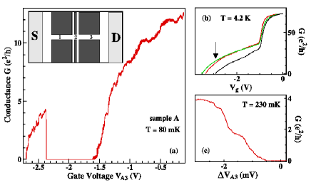
shows a typical example of CC1 at 0.1 K, where wire 1 of sample A (A1) was fixed at V corresponding to several occupied 1D subbands, and is measured as a function of . Figure 1(b) shows the characteristics of the two wires A1 and A3, measured independently as well as in series. The arrow indicates the voltage (-2.91 V) at which wire A1 is fixed for the measurement in figure 1(a). When A1 is biased at this voltage, the series combination of A1 and A3 together pinch-off at V, as shown in figure 1(a). As was swept towards 0 V, the two-terminal conductance rose to a value close to and abruptly collapsed to zero (within the measurement noise level) at V. The drop in the conductance is more than three orders of magnitude. On continuing the voltage sweep, the conductance increases gradually from zero for V. In a slow sweep of (different measurement), shown as figure 1(c), the collapse edge shows a plateau at . At low temperatures, the zero conductance state is stable and lasts for several days until the experiment is terminated. At higher temperatures, the conductance drops to a value above zero, but the drop is still abrupt. No such collapse has been observed in a single wire.
To highlight the reproducibility of CC1 in the up sweeps and the absence of it in the down sweeps, we show in figure 2(a)
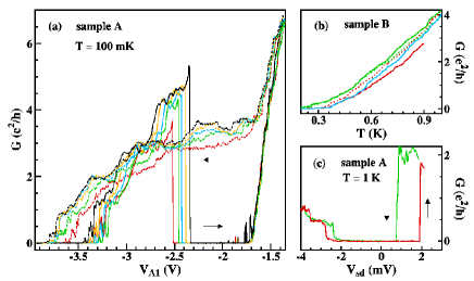
five sets of measurements taken under the same conditions. Here is fixed at V and is swept. The conductance collapse is only observed in the up sweeps (solid lines) for V V, whereas the conductance for the down sweeps (dashed lines) remains finite, close to , for the same range of . The large hysteresis in the characteristics of the up and down voltage sweeps is a feature of CC1. We note that for either direction of sweep, the characteristics to the left of the collapse ( V) in figure 2(a) are not exactly reproduced in all the traces, but to the right of the collapse ( V) they are nearly identical. A change in pinch-off voltage accompanies a change in collapse voltage for different sweeps. Traces with a more negative pinch-off voltage have a conductance collapse at a less negative voltage and from a higher conductance value. With gate voltages fixed in the collapse region for sample B, figure 2(b) shows the reproducibility of a typical collapse state in several temperature cycles between 0.2 and 1 K.
Figure 2(c) shows the DC source-drain bias measurements taken in the collapse region for sample A at 1 K. At , the collapse state was stable at for K. As increases, we observe a sudden jump in the conductance from zero to a nearly constant value, indicative of a gap in the density of states or depinning. The gap shows hysteresis and a jump to a different value for and . The gap, 3–5 mV, is much greater than both the highest temperature at which any collapse is observed and the activation temperature of 5.5 K measured in this cooldown.
Transverse magnetic field measurements show that the collapse is accompanied by a reduction in the 1D carrier density with decreasing temperature. The effect of a transverse magnetic field on 1D wires is to increase the energy spacing of the 1D subbands and cause them to pass progressively through the Fermi energy berggren86 . The energies of the magnetoelectric 1D levels are determined by the confinement provided by the gate voltages and the magnetic field. At a constant gate voltage, as in our case, magnetic depopulation causes to decrease as is increased, with plateaus of quantized conductance appearing as the energy levels are forced through the Fermi energy. When the cyclotron diameter is greater than the wire width the levels are hybrid magnetoelectric levels, and when the cyclotron diameter is much less than the width the 1D subbands are equivalent to 2D Landau levels berggren86 . From the filling factor of Landau levels, the electron density can be extracted. Figure 3(a)
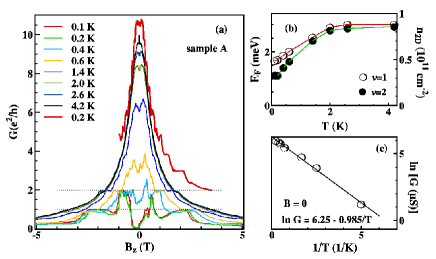
shows the magnetoconductance at various temperatures for sample A in the collapse region with fixed gate voltages on each of the three wires. As decreases, at decreases and there is a decrease in the magnetic field required to depopulate a particular subband. For example, at 4.2 K the conductance plateau occurs at T, but at 0.4 K the plateau shifts to 1 T, corresponding to a 50% reduction in the (2D) carrier concentration, or an equivalent drop in the Fermi energy, shown in figure 3(b).
Starting from the collapse region, a perpendicular field of 200 mT is sufficient to restore conductance. For K, the conductance first rises to a value close to with increasing . The thick red trace in figure 3(a) shows measured at 0.2 K but outside the collapse region. The depopulation trace is almost identical with that measured in the collapse region at 4.2 K (black trace), indicating that the carrier density is restored on heating and showing that the drop in carrier concentration is a property solely of the long wire structure formed from the two in series. Figure 3(c) shows an Arrhenius plot of from figure 3(a), with an activation temperature of 1 K.
The second type of collapse, CC2, observed in the presence of an in-plane magnetic field, is reproducible in both directions of gate voltage sweep. Figure 4
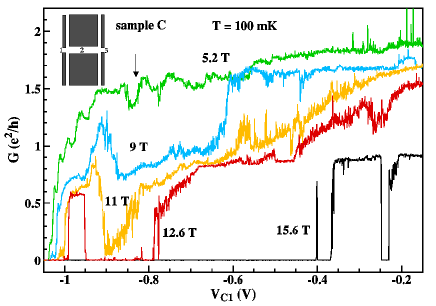
shows five traces in sample C at various in-plane magnetic fields, , applied parallel to the wires. The misalignment of the field was less than 1∘ out of the 2DEG plane. For this measurement is such that at . Strong fluctuations are present in the traces. As increases, a small valley at T marked by an arrow drops to zero conductance at T, and the width of the collapse region increases. At T, the valley expands and a new region of collapse is seen at V. The conductance drop is typically and the gate voltage width of the collapse was within broadening of zero. The collapse was continuously reproduced in both sweep directions over 100 times with no appreciable change in the traces. Shifting the short wire C1 laterally has no appreciable effect. Collapse type CC1 was also observed in this sample, but reproducibility was low. It is unknown whether the reproducibility of CC2 in the up anddown sweeps, in contrast to CC1, is associated with the lifting of the spin degeneracy of the electrons.
Traces of CC2 at different temperatures at 12.6 T are shown in figure 5.
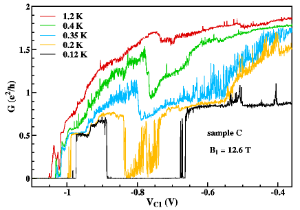
At 0.12 K the collapse is well defined, and outside the collapse region the conductance is suppressed to . At 1.2 K strong fluctuations set in, the collapse is removed, and there is no spin-split plateau at . The disappearance of the spin-split plateau and the associated rise in at high temperatures resemble our previous observations on the 0.7 structure thomas00 .
Various mechanisms can be responsible for small drops in conductance. Resonances, resulting from defects, impurities, or modifications of the exit regions; universal conductance fluctuations BeenRev ; and for double constrictions, anti-resonances due to mode matching blaikie are possible. These mechanisms, however, cannot explain collapses of the magnitude observed here, nor the hysteresis and temperature dependences. Localization of carriers by disorder is inconsistent with figure 2(c). No anomalies were reported in previous studies of short wires in series wharam88b ; kouwen89 .
Theories exist which predict the existence of an insulating state in 1D wires. In the presence of any scattering the conductance of a Luttinger liquid is expected to vanish as a power law in temperature and voltage. The observed behaviour (figure 2(c)) is inconsistent with such a mechanism. An insulating state may result from the pinning of a Wigner crystal or a charge density wave by a barrier potential. The relation and thermally activated behaviour support such mechanisms glazman92 . Our 2D density immediately before the collapse is cm-2. For a width of 0.3 m, equal to the cyclotron diameter at 0.2 T, where the collapse is removed in figure 3(a), we estimate cm-1 or , being the Bohr radius. At such low densities a 1D Wigner crystal glazman92 ; schulz93 in single subband wires is expected, and may show a pinning energy greater than the thermal activation energy, as we observe. A trapped superconducting state lambert98 also cannot be excluded. For multiple subbands, an inter-subband charge density wave starykh could open a gap at the Fermi level due to inter-subband backscattering, leading to an insulating state. However, the drop in Fermi energy with temperature further suggests the formation of a state below the 1D subbands as . We also note the suppression of the collapse with a small perpendicular field, which suggests that the interaction between k and k electrons is important.
In summary we have observed an unusual collapse in the conductance of serially connected 1D quantum wires. Two types of collapse are observed, both of which have the defining feature of zero conductance in a gate voltage region where a finite conductance is expected. The mechanism is unknown but may result from an inter-subband charge density wave or a 1D Wigner crystallization. Further experimental and theoretical work is necessary to understand the phenomenon.
We acknowledge EPSRC for funding this work, and KJT thanks the Royal Society for the Eliz Challenor Research Fellowship. We thank Alan Beckett and Pete Flaxman for technical assistance.
References
- (1) S. Tomonaga, Prog. Theor. Phys. 5, 544 (1950).
- (2) J. M. Luttinger, J. Math. Phys. 4, 1154 (1963).
- (3) F. D. M. Haldane, J. Phys. C 14, 2585 (1981).
- (4) C. L. Kane and M. P. A. Fisher, Phys. Rev. B 46, 15233 (1992).
- (5) L. I. Glazman, I. M. Ruzin, and B. I. Shklovskii, Phys. Rev. B 45, 8454 (1992).
- (6) H. J. Schulz, Phys. Rev. Lett. 71, 1864 (1993).
- (7) A. I. Larkin and P. A. Lee, Phys. Rev. B 17, 1596 (1978).
- (8) K. Kuroki and H. Aoki, Phys. Rev. Lett. 72, 2947 (1994).
- (9) O. A. Starykh, D. L. Maslov, W. Häusler, and L. I. Glazman, Low-Dimensional Systems: Interaction and Transport Properties (Springer, 2000), pp. 37–78, cond-mat/9911286.
- (10) D. L. Maslov and M. Stone, Phys. Rev. B 52, 5539 (1995).
- (11) I. Safi and H. J. Schulz, Phys. Rev. B 52, 17040 (1995).
- (12) V. V. Ponomarenko, Phys. Rev. B 52, 8666 (1995).
- (13) K. J. Thomas, J. T. Nicholls, M. Y. Simmons, M. Pepper, D. R. Mace, and D. A. Ritchie, Phys. Rev. Lett. 77, 135 (1996).
- (14) A. J. Daneshvar, C. J. B Ford, A. R. Hamilton, M. Y. Simmons, M. Pepper, D. A. Ritchie, Phys. Rev. B 55, 13409 (1997).
- (15) A. C. Graham, K. J. Thomas, M. Pepper, N. R. Cooper, M. Y. Simmons, and D. A. Ritchie, Phys. Rev. Lett. 91, 136404 (2003).
- (16) S. Tarucha, T. Honda, and T. Saku, Sol. St. Commun. 94, 413 (1995).
- (17) C.-T. Liang, M. Pepper, M. Y. Simmons, C. G. Smith, and D. A. Ritchie, Phys. Rev. B 61, 9952 (2000).
- (18) W. Apel and T. M. Rice, Phys. Rev. B 26, 7063 (1982).
- (19) M. Ogata and H. Fukuyama, Phys. Rev. Lett. 73, 468 (1994).
- (20) M. Bockrath, D. H. Cobden, J. Lu, A. G. Rinzler, R. E. Smalley, L. Balents, and P. L. McEuen, Nature 397, 598 (1999).
- (21) K.-F. Berggren, T. J. Thornton, D. J. Newson, and M. Pepper, Phys. Rev. Lett. 57, 1769 (1986).
- (22) K. J. Thomas, J. T. Nicholls, M. Pepper, W. R. Tribe, M. Y. Simmons, and D. A. Ritchie, Phys. Rev. B 61, 13365 (2000).
- (23) C. W. J. Beenakker and H. van Houten, in Solid State Physics, edited by H. Ehrenreich and D. Turnbull (Academic Press, New York, 1991).
- (24) K. Nakazato and R. J. Blaikie, J. Phys.: Cond. Matt. 3, 5729 (1991).
- (25) D. A. Wharam, M. Pepper, H. Ahmed, J. E. F. Frost, D. G. Hasko, D. C. Peacock, D. A. Ritchie, and G. A. C. Jones, J. Phys. C 21, L887 (1988).
- (26) L. P. Kouwenhoven, B. J. van Wees, W. Kool, C. J. P. M. Harmans, A. A. M. Staring, and C. T. Foxon, Phys. Rev. B 40, 8083 (1989).
- (27) C. J. Lambert and R. Raimondi, J. Phys. C 10, 901 (1998).