Foil-based atom chip for Bose-Einstein condensates
Abstract
We describe a novel method of fabricating atom chips that are well suited to the production and manipulation of atomic Bose-Einstein condensates. Our chip was created using a silver foil and simple micro-cutting techniques without the need for photolithography. It can sustain larger currents than conventional chips, and is compatible with the patterning of complex trapping potentials. A near pure Bose-Einstein condensate of 4 104 87Rb atoms has been created in a magnetic microtrap formed by currents through wires on the chip. We have observed the fragmentation of atom clouds in close proximity to the silver conductors. The fragmentation has different characteristic features to those seen with copper conductors.
pacs:
3.75.-b, 34.50.Dy1 Introduction
Bose-Einstein condensates (BECs) have become a valuable tool for probing many aspects of atomic and quantum physics. Recently, condensates have been produced in miniature magnetic traps formed by current-carrying wires patterned onto a substrate [1, 2]. Such devices have become known as atom chips, and are finding wide application in efforts to coherently control matter for new atom-optical devices [3].
Atom chip BEC experiments have mostly been performed with chips fabricated using photolithographic techniques [4, 5, 6]. These chips have been highly successful and form the basis of a growing number of experiments. However, there are some limitations to chips produced in this manner. One is that the photoresist thickness and etching process constrain the maximum height of the conducting wires. Typical conductor thicknesses range from about m for evaporatively or sputter-coated wires, up to m for electroplated wires. The latter also appear to suffer from rough edges, leading to fragmentation of clouds near the surface [7]. A desirable feature of atom chips is that narrower wires result in tighter trapping potentials near the surface for a fixed current. However, the cross-sectional area (and hence the thickness) of a wire restricts the maximum current that can be sustained before it overheats and detaches from the surface. Current densities of order A cm-2 have been achieved on atom chips at currents of order 1 A, but continuous operation at these current densities is fraught with danger. An elegant solution to this problem would be to use high- superconducting wires, although this introduces additional technical complexity. Thicker extruded wire [8] and machined copper conductors [9] have also been used to obtain higher currents, but these methods are not suited to sub-millimetre patterning.
In this article we describe a method of fabricating atom chips with thick wires capable of sustaining currents of several amps without overheating. We begin by reviewing magnetic microtraps and provide analytic expressions to describe the properties of the widely used Z-wire trap. We then describe the fabrication process for our chip and demonstrate its effectiveness by using it to produce a Bose-Einstein condensate of 87Rb. Finally, we look at cold atom clouds trapped close to the chip surface and observe fragmentation of the atomic density profile.
2 Magnetic Microtraps
When an atom with a magnetic dipole moment, , is placed in a magnetic field, , it experiences an interaction potential = - . If the projection of the magnetic moment onto the field remains constant during the atom’s motion, the adiabatic condition is satisfied (i.e. the atom remains in the same magnetic substate, ). In such cases the potential is given by the scalar expression, = -, where is the Landé g-factor, is the Bohr magneton and = . Atoms whose magnetic moment aligns antiparallel to are known as weak-field seekers, as their lowest energy state is at a minimum of .
Several arrangements of wires have been proposed [10] and used in experiments to realise a variety of magnetic trapping geometries for weak-field seeking atoms [11, 3]. A building block for all of these is the “side guide”, in which the combination of the field of a straight conducting wire and homogeneous bias field produces a two-dimensional, linear (to first order) trapping potential. A simple three-dimensional trap can be realised by bending a single wire into the shape of a Z, as shown in figure 1, where the top and bottom wire sections produce a confining potential in the longitudinal () direction.
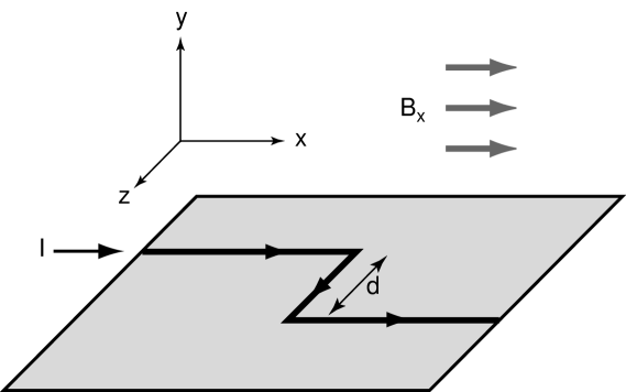
The combination of a Z-shaped wire and transverse bias field, , produces a Ioffe-Pritchard type trap with a nonzero minimum located above the centre of the middle section of wire. In the - plane the trap minimum is where the field of the wire is exactly compensated by the bias field . While the and components of the field go to zero here, the -component, , is nonzero out of the plane of the chip ( = 0), as the fields due to the two sections of current in the -direction add constructively. Treating the wires as having an infinitesimal cross-section, the distance from the wire to the minimum is given by
| (1) |
where is the magnetic permeability of free space and is the current through the wire. The magnitude of the field gradient near the minimum (,,) = (0,,0) is equal in the radial ( and ) directions, and is given by
| (2) |
In the axial () direction the trapping potential is well described by half of the -component of field produced by two infinite wires carrying current in the -direction, located at (,) = (0,). The trapping potential is given by
| (3) |
which is approximately harmonic at the centre with a curvature
| (4) |
The residual offset field in the direction at the minimum of the trap is
| (5) |
which can be partially compensated by an additional field along - to increase the transverse confinement.
3 Atom Chip
Our atom chip was fabricated entirely in-house using materials and machinery readily available to typical laboratories. A schematic of the chip is shown in figure 2.
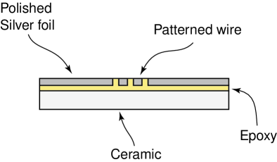
A 125 m silver foil (Goodfellow AG000360) was glued onto a 1 mm thick machinable ceramic (Macor) substrate using EpoTek H77 ultra high vacuum (UHV) compatible epoxy. Silver was chosen as the conductive material as it has the lowest resistivity of all metals (1.59 cm), compared with gold (2.2 cm) and copper (1.67 cm). It is also highly reflective (97%) to light resonant with the Rb D2 transition at 780 nm. The epoxy adheres strongly to the ceramic, but less effectively to the silver. Improved bonding to the silver was achieved by roughening the surface to be glued with fine-grade sand paper. A 100 nm platinum layer was evaporatively coated onto the foil, which was then oxidised (with heat in air) before gluing. After curing the epoxy, the foil was polished to a mirror finish in three stages. Firstly, fine-grade abrasive paper held on a flat block was used under running water to take out any large ( 10 m) ripples in the surface. Secondly, a range of finer grade abrasive cloths (Micromesh 1500 – 8000) were used down to a grain size of 3 m. Finally, 3 m and 1 m grain size diamond polishing pastes (ProSciTech M23/3 and M23/1) were applied to the surface with a silk polishing cloth. These three polishing stages typically removed about 30 – 40 m of the silver, leaving a final conductor thickness of approximately 90 m. The finished surface had very few scratches visible to the naked eye. A near-infrared laser beam was reflected from the finished surface and viewed several metres away without visible distortion. The power in the reflected beam was 95 2% of the incident power, in good agreement with the known reflectivity of silver at 780 nm.
The polished chip was then ready to be machined. A computer numerically controlled (CNC) milling machine was used to cut insulating gaps into the silver foil using a 150 m diameter PCB cutting tool (LPKF 0.15 mm end mill, 107244). The wire patterns were programmed into the CNC mill and the cutting was performed in several runs, with the cut depth incremented by 20 m each run. The cutting tool spun at 10 krpm and traced the pattern of the wires at a speed of 5 mm/min. We found these parameters gave good results, but expect that higher rotation rates would be desirable. Deeper cutting increments (up to 50 m) were also tried and no noticeable degradation of the cuts were observed. However, the tool was seen to wear very quickly if it penetrated the ceramic and so we were cautious with our increments. Small holes (1 mm diameter) were drilled through the foil, epoxy and macor near the edges of the chip, in the centre of the current connection pads.
After the pattern was cut, the resulting insulating channels were carefully backfilled with epoxy to provide additional mechanical support and heatsinking for the wires. Finally, the whole chip was repolished using the diamond pastes to remove any scratches or residues from the cutting process. The chip was cleaned with distilled water and methanol, before the electrical connections were assembled and the chip was placed in the vacuum chamber.
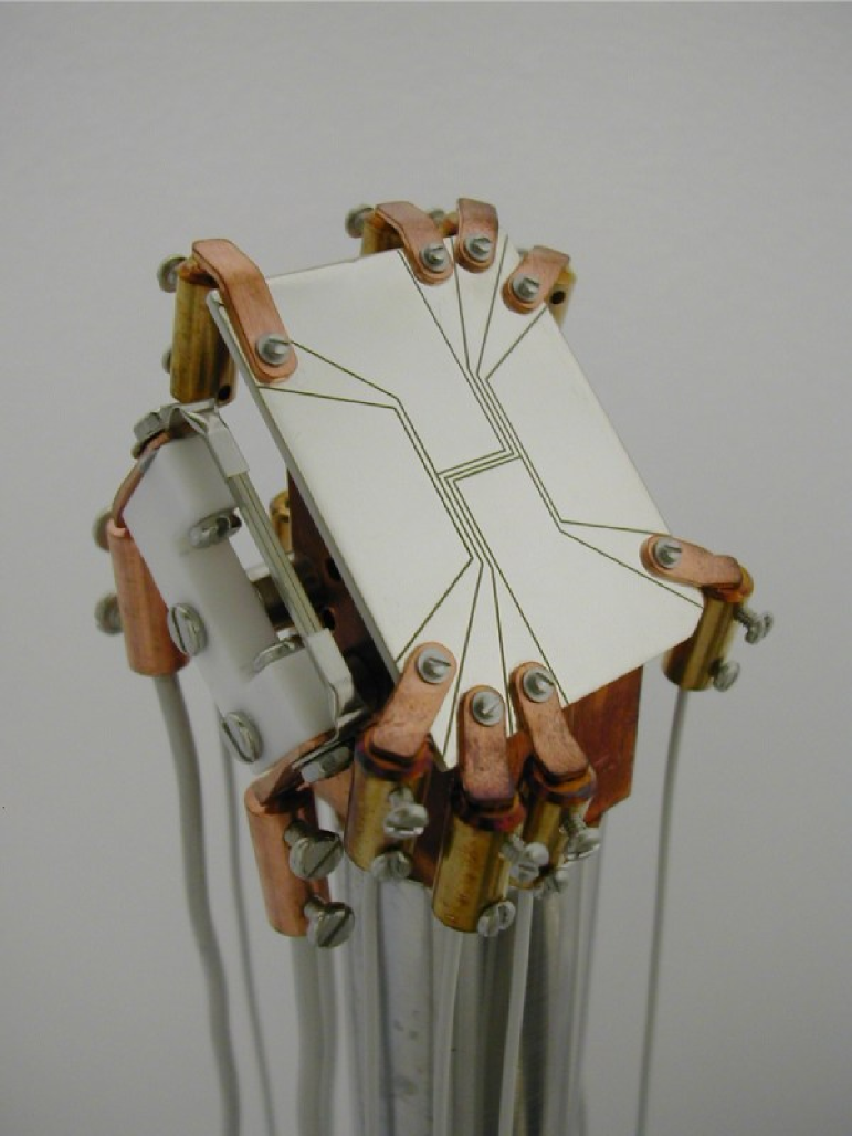
The robust nature of our chip allows simple yet secure electrical connections to the wires. The holes drilled through the connection pads accommodate 1 mm diameter screws. Copper tabs, also with holes drilled through them, were placed onto the connection pads and held in place by screws with a nut and sprung washer that prevented loosening during bake-out of the vacuum system. By contacting over a large area of the pad we ensure very low resistance connections and negligible heating. Figure 3 shows the completed chip with the electrical connections in place. The copper tabs are attached to barrel connectors, which in turn connect to thicker ceramic coated wires (Kurt J. Lesker, CCWA10SI and CCWA20SI) that run to the electrical feedthroughs for the vacuum chamber. Also visible is the rubidium dispenser, attached to the side and recessed by a few millimetres from the silver surface of the chip.
We have tested the current-carrying capacity of our chip wires and found that individual wires can sustain currents of 8 A in vacuo for 10 s with the temperature remaining below 100 ∘C. The temperature was evaluated by monitoring the resistance of the wire from outside the vacuum chamber. This necessarily includes the resistance of the connections and connecting wires — our estimate of the heating assumes that the increase in resistance observed was entirely due to heating of the chip wires. We therefore obtain an upper limit for the temperature increase of the chip. A nude ion gauge located approximately 30 cm from the chip could detect no increase of the pressure in the vacuum chamber at the level of 2 10-11 mbar during these measurements. The current density in the wire was 5 104 A cm-2.
Figure 3 also shows the wires patterned onto the chip. These consist of two parallel Z-trap wires with a centre to centre separation of = 0.4 mm, and two additional endcap wires for varying the axial confinement. The parallel Z-wires are capable of producing fields suitable for realising the two-wire guide proposed in [12]. Assuming equal currents in the two wires, there are three possible configurations in the - plane. These can be selected by the strength of the (dimensionless) bias field, =, where = . The first, 1, consists of two quadrupole traps in the = 0 plane, separated vertically by . The second is a single hexapole trap which occurs at the critical bias field value ( = 1), with a minimum at (,) = (0,). The third configuration is for 1 and produces two symmetric traps separated horizontally by .
4 Experiment
We have used our atom chip to produce Bose-Einstein condensates of 87Rb atoms. The experiment follows the usual stages for BEC production and the details of our procedure are described below.
Our vacuum chamber consists of a glass cell (made in our glass-blowing workshop) attached to a stainless steel vacuum chamber. We use a 75 l/s ion pump and a non-evaporable getter to reach pressures below mbar. This was achieved by baking the chamber for two weeks at a temperature of 140 ∘C and pumping it with a turbo pump. The epoxy bonding the silver to the ceramic is rated to 150 ∘C which limits the bake-out temperature.
Rubidium vapour is obtained from a dispenser source which is pulsed with a current of 7.2 A for 12 s. We collect 108 atoms in a reflection magneto-optical trap (MOT) formed 4.5 mm from the surface of the chip. Trapping light is provided by a Toptica DLX 110 400 mW external cavity diode laser system sent through a single mode fibre. It is tuned 15 MHz below the 5S1/2 = 2 to 5P3/2 = 3 transition in 87Rb. Four trapping beams enter the chamber, each with a power of 23 1 mW and 1/e2 diameter of approximately 25 mm. This laser is a home-built external cavity diode laser system locked to the = 1 to = 2 transition. The repump laser is combined with the trapping laser on a polarising beam splitter cube, and approximately 10 mW of repump light enters the chamber.
After the dispenser pulse, atoms are held in the MOT for a further 10 s to allow the vacuum to recover. At this distance from the surface the MOT does not appear to be seriously depleted by the imperfections in our mirror due to the insulating gaps. While we cannot make a direct comparison with a MOT with a near perfect mirror, our atom number (108), temperature (90 K) and lifetime (40 s) are sufficient for producing condensates.
Next, the atoms are transferred to a compressed MOT with a magnetic field provided by a U-shaped wire centred 1.6 mm below the silver surface carrying a current of 20 A, combined with a uniform transverse bias field of 12 G. This results in a spherical quadrupole field with gradients of 35 G cm-1 radially and 5 G cm-1 axially leading to a highly anisotropic cloud at a distance of 1.5 mm from the chip surface. The MOT lasers and current through the U-wire are then turned off simultaneously in less than 100 s and the atoms are optically pumped into the = 2, = 2 ground state in 400 s. A current of 4 A is then turned on through both Z-wires on the chip and the atoms are caught in the potential produced by the wire and a 12 G transverse bias field. The bias is ramped linearly from 12 G to 30 G over 500 ms to compress the cloud and achieve final trapping frequencies of 570 Hz radially and 11.2 Hz axially at a distance of 430 m from the surface. The lifetime of atoms in the magnetic trap is more than s, indicating that the vacuum is not adversely affected by the chip. At this point efficient evaporative cooling can begin.
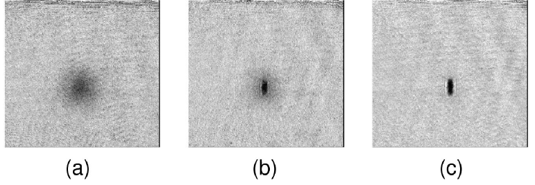
The atomic cloud is evaporatively cooled through the BEC transition using a single logarithmic sweep of a radio frequency (RF) magnetic field from 13 MHz to around 1 MHz in 10.5 s. In the two-wire trap this produces condensates of around 3 104 atoms. Larger condensates can be produced by further compressing the cloud into a trap formed by current through a single wire. Figure 4 shows absorption images of atom clouds following 15 ms free expansion after being released from a single wire magnetic trap. The three images show clouds after terminating the RF evaporation at 1080 kHz, 1050 kHz and 1010 kHz respectively. The trap forms 200 m from the chip surface with oscillation frequencies of 1100 Hz radially and 6 Hz axially. The condensate contains around 5 104 atoms and has a peak density of 4 1014 cm-3. With our parameters the critical temperature for condensation is around 500 nK, which is reached with approximately 1.2 105 atoms.
5 Fragmentation
When cold atom clouds are brought close to current-carrying wires, the atomic distribution is seen to fragment into “lumps” [13, 14, 15]. This is apparently due to microscopic deviations in the direction of current flow which produce small components of magnetic field parallel or antiparallel to the axis of the wire [13]. This effect may prove to be a limitation of current-carrying wire-based atom chips for applications such as atom interferometry.
We also observe fragmentation of cold clouds brought close to the chip surface. Figure 5 shows an absorption image and an averaged cross-sectional profile of a fragmented atom cloud after being accelerated away from the chip surface. The cloud was prepared at a distance of 45 5 m from a single wire at a temperature of 4 K. At this distance the atoms could not be directly viewed in the trap due to light scattered from the gaps between the wires. Therefore the atoms were accelerated away from the surface for 5 ms by ramping up the current through the wire immediately before being imaged. Because of the short acceleration time and low cloud temperature and axial trapping frequency (nominally 2.9 Hz), any redistribution of atoms in the axial direction in the displaced trap is not significant in the image.
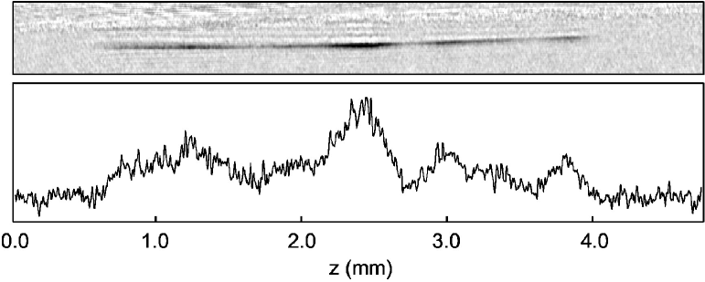
We observe larger structure in the atomic density profile than has been seen in other experiments — up to the millimetre scale. The cross-sectional profile also reveals shorter wavelength structure superposed on these larger fragments. This may be caused by slight deviations in the movement of the cutter during milling producing wires that are not perfectly straight — however we have no direct evidence of this as yet. The depth of the fragmenting potential is comparable to what has been seen above copper conductors [15].
Fragmentation appears to be highly dependent on the geometric and material properties of the conductors [7]. Our method of chip fabrication may be beneficial in this regard, as the high-purity solid metal foil should have superior conductor uniformity to electroplated wires. It remains to be seen how precisely wires can be patterned into a solid foil, and subsequently how this affects fragmentation. This topic will be investigated in future work. Regardless of any improvements in uniformity, our higher current-carrying capacity allows us to produce moderately tight traps further away from the conductors. This is important as fragmentation is seen to scale approximately as , where is the wavenumber of the current deviations [15].
6 Conclusion
We have demonstrated a novel method of producing atom chips suitable for the production and manipulation of Bose-Einstein condensates. Our chip is capable of sustaining higher currents than typical lithographically patterned chips, and can therefore produce deeper magnetic traps. This facilitates condensate production without sacrificing the versatility of the atom chip. The patterning of wires on our chip is currently at the 100 m scale but could be reduced using laser cutting to produce the insulating channels. Nonetheless, our technique has proven to be simple and reliable. Because of the higher current-carrying capacity of this setup, we are able to produce moderately tight traps at distances greater than 100 m from the surface, where fragmentation effects become less important.
References
References
- [1] Ott H, Fortagh J, Schlotterbeck G, Grossmann A and Zimmermann C 2001 Phys. Rev. Lett. 87 230401
- [2] Hänsel W, Hommelhoff P, Hänsch T W and Reichel J 2001 Nature 413 498
- [3] Folman R, Krüger P, Schmiedmayer J, Denschlag J and Henkel C 2002 Adv. Atom. Mol. Opt. Phys. 48 263
- [4] Hänsel W, Reichel J, Hommelhoff P, and Hänsch T W 2001 App. Phys. B 72 81
- [5] Fortágh J, Ott H, Schlotterbeck G, Zimmermann C, Herzog B and Wharam D 2002 App. Phys. Lett. 81 1146
- [6] Leanhardt A E, Chikkatur A P, Kielpinski D, Shin Y, Gustavson T L, Ketterle W and Pritchard D E 2002 Phys. Rev. Lett. 89 040401
- [7] Estéve J, Aussibal C, Schumm T, Figl C, Mailly D, Bouchoule I, Westbrook C and Aspect A 2004 Preprint physics/0403020
- [8] Jones M P A, Vale C J, Sahagun D, Hall B V and Hinds E A 2003 Phys. Rev. Lett. 91 080401
- [9] Schneider S, Kasper S, vom Hagen Ch, Bartenstein M, Engeser B, Schumm T, Bar-Joseph I, Folman R, Feenstra L and Schmiedmayer J 2003 Phys. Rev. A 67 023612
- [10] Weinstein J D and Libbrecht K G 1995 Phys. Rev. A 52 4004
- [11] Hinds E A and Hughes I G 1999 J. Phys. D. 32 R119
- [12] Hinds E A, Vale C J and Boshier M G 2001 Phys. Rev. Lett. 86 1462
- [13] Kraft S, Günther A, Ott H, Wharam D, Zimmermann C and Fortágh J 2002 J. Phys. B 35 469
- [14] Leanhardt A E, Shin Y, Chikkatur A P, Kielpinski D, Ketterle W and Pritchard D E 2003 Phys. Rev. Lett. 90 100404
- [15] Jones M P A, Vale C J, Sahagun D, Hall B V, Eberlein C C, Sauer B E and Hinds E A 2004 J. Phys. B 37 L15