Shell-effects in heavy alkali-metal nanowires
Abstract
We supplement our previous observations of the shell effect in alkali-metal nanowires (Li, Na, K) shell ; atomic ; FNT ; super with data extended to the heavy alkalis Rb and Cs. Our observations include: i) a non-monotonous dependence of conductance-histogram peak heights on atomic weight, ii) a rapid transition to an atomic shell structure at elevated temperatures, and iii) a ”reverse” atomic-electronic shell transition, caused by the closeness to the liquid state.
I Introduction
Conductance quantization was first observed in a 2-dimensional electron gas in a semiconductor heterostructure Wees . Later the effect was extended to a 3-dimensional electron gas in metals using nanowires produced by the break-junction technique Krans . The alkali metals used in the latter study have a single valence electron very weakly bound to the nuclei. They are well suited to satisfy the free-electron gas model. It has been long known that for clusters of alkali metals the conduction electrons are spherically distributed around the ions, smoothing the corrugation of ionic roughness. In a nanowire this leads to a cylindrical shape of the binding potential for finite electron movement in transverse dimensions. For thicker nanowires, the side surface becomes faceted. This transformation is stipulated by elevated temperatures, where the ions occupy the positions corresponding to a minimum of the lattice free energy.
At helium temperatures nanowires obtained by the break-junction technique assume all possible diameters, down to a single atom in cross-section, on many times stretching and renewing the contact between massive electrodes. The summation of conductance versus elongation traces (we call these “scans”) yields a conductance histogram whose peaks indicate the enhanced stability of nanowires with given diameters (conductance). These diameters correspond to a “magic” number of atoms in the narrowest cross-section whose conductance electrons fully occupy the so-called electron-energy shells in the transverse dimensions deHeer ; shell . By shells we imply the bunches of electron energy levels in the 2-dimensional cross-section whose positions on the energy scale are separated from each other by much wider energy gaps.
At elevated temperatures the probability of observing the electronic “magic” diameters becomes greatly enhanced, since the atoms have enough mobility to occupy the “magic” cross-section during subsequent rearrangements, which relax the strength created by pulling. Accordingly, the shell structure is greatly enhanced with rising temperature.
As in metallic clusters, the amplitude of electronic shell oscillations in thicker nanowires decreases with radius and the geometric (atomic) oscillations take over. The side surface becomes faceted and a complete layer of atoms (or a completed facet) corresponds to the enhanced stability of the nanostructure (cluster or wire) Martin ; atomic . There is an important difference between clusters and nanowires. While in the first case atoms on the surface are exchanged with the gas phase in the mass spectroscopy device through evaporation or condensation, in the second one the surface atoms are exchanged with the banks by surface diffusion and mechanical deformation during stretching of the wire on pulling. This imposes additional geometrical constraints to which the geometric shell structure should be compatible FNT . This is observed when recording return-histograms, which differ from the usual ones that are built from scans in the forward (pulling) direction, in being collected while applying a pushing force to compress the wire (in reverse movement).
In the present paper we extend the previous studies of conductance quantization, electronic shell/supershell and atomic (geometric) shell effects in Li, Na, and K shell ; atomic ; FNT ; super to the heavy alkali metals Rb and Cs. We supplement our data with a number of new observations, among them are: i) a non-monotonous succession of peak heights in the conductance histogram against the atomic weight in the series LiNaKRbCs; ii) the evolution of conductance histograms and their Fourier spectra as a function of temperature; iii) the reverse transition from atomic to electronic shell oscillations at the highest attainable temperature for the heaviest alkali Cs, which we connect with the liquid state of the nanowire.
II Low-temperature conductance histograms
Conductance histograms for the five alkali metals measured by us, and their atomic weights and melting points are shown in Fig.1.
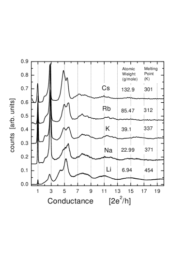
All of them exhibit conductance quantization for electron wave functions propagating along a metallic waveguide with circular cross-section of variable radius Krans . The peaks near conductances equal to 1, 3, 5 and 6 conductance quanta are clearly seen. Note that peaks at =2, and 4 are (almost) absent. For Na and K the peak heights at =1, 3 are approximately equal (Fig.2) while for Li the peak at 1 is always lower than that at 3.
For the heaviest metals Rb and Cs this behavior could be understood in terms of the atomic mobility in a one-atom contact, taking into account their noticeably lower melting point, but for Li it seems strange. Another anomaly for Li is the much higher shift of the peak positions at 5 and 6 to lower conductances. Presumably, the mobility of the Li atoms is higher than that of Na and K even at helium temperatures, in spite of its higher melting point. This could be due to tunnelling of the light Li atoms through shallow barriers in the case where the number of interatomic bonds is greatly reduced. This could be tested by measurements at still lower temperatures where tunnelling of atoms would be seen as a temperature independent height of the first peak.
The intense peaks at =1, 3, 56 should be distinguished from the shallow maxima at 8, 11, 15 … (Fig,1), which are due to the low-temperature electronic shell structure. Below we shall show how such a structure evolves with rising temperature, but here we note that the shell structure extends down even for the conductance peaks at =3 and 56. Especially this is evident for , which according to calculation for Na Torres should be much smaller than 6, and according to the experiment given in Ref.Bas, does not carry a fully open conductance channel as that of =6. From the data presented in Fig.1, the intensity of the peak near =5 is of the same order as that near 6, and increases (compared to the peak at 6) in the direction NaCs, according to the lowering of the melting point. In other words, the increased mobility of the atoms (due to the melting point lowering) stimulates the shell-effect contribution to the peak at 5 in the same way as a rise in the temperature affects other shell-structure peaks (8, 11, 15, etc.).
III Rubidium
III.1 Shell and supershell structure
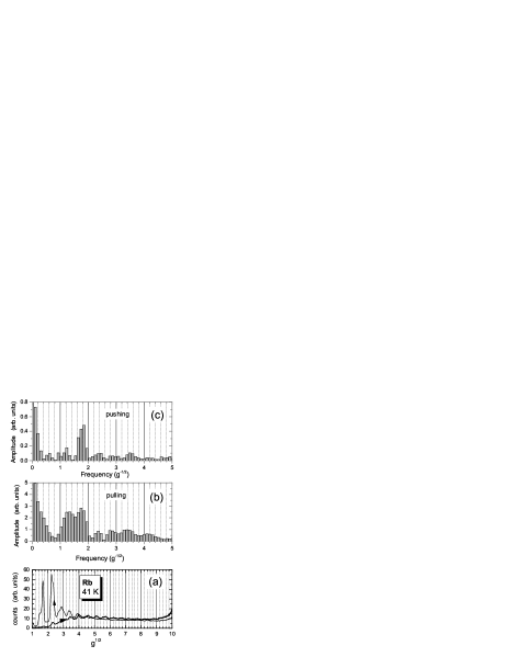
Conductance histograms for Rb both for pulling (i.e. decreasing) and pushing ( increasing) force are shown in Fig.3 (a).
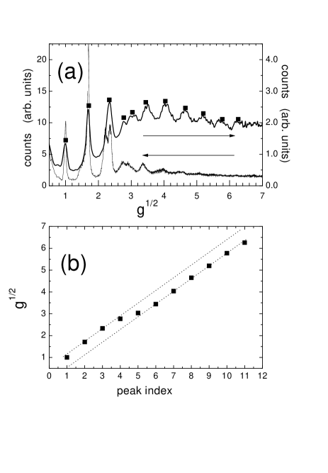
The histograms are obtained by cycling a Rb contact many times between =100 and 0.2. Along the abscissa we use the square root of since for this coordinate the shell oscillations are expected to be periodic, and we find a period shell (Fig.3 (b)). This period is close to the average periodicity predicted by quasi classical calculation for triangular and rectangular orbits in circular cross section FNT . There is a noticeable difference between the regular (pulling) and return (pushing) histograms. The observed hysteresis signifies that not only the equilibrium temperature influences the atomic movement, but the dynamics of atomic rearrangement itself strongly determines the observed histograms. In particular, the visible number of shell oscillations while pushing is substantially greater than that for pulling force (see the symbol positions which mark the oscillation maxima in Fig.3 (a)). The peak heights in the return histogram follow the shell oscillation envelope more smoothly, than those in the regular one.
Around peak indices a shift of the straight line fit is observed. This may be a phase-shift due to the node of shell oscillation amplitude (the so-called, supershell effect super ).
For completeness we show the Fourier spectrum for the return histogram of Fig.3 (a). A smooth background is subtracted (see Fig.4 (a)) for clarity.
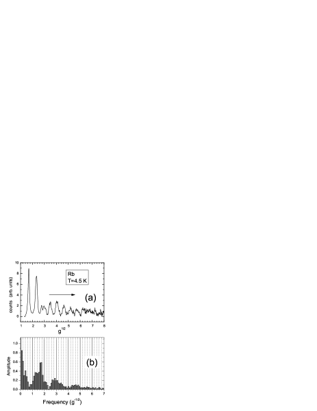
The spectrum in Fig.4 (b) displays two principal maxima at frequencies and 1.7 which are characteristic of the electronic shell effect, where the triangular and rectangular trajectories are seen as a single maximum at and the diametrical trajectory appears as a maximum at . The structure at higher frequencies may be considered as harmonics of the principal spectrum.
III.2 Evolution of the shell structure with temperature
Up to a temperature of 40 K the electronic shell effect prevails in the conductance histogram. An example of this is shown in Fig.5. The peaks at and 1.8, characteristic of the electronic shell oscillations, are the strongest ones in the forward (pulling, Fig.5 (b)) and return (pushing, Fig.5 (c)) Fourier spectra. The enhanced mobility of the Rb atoms stimulated by increasing temperature leads to a maximum intensity of the peak at 2.3 relative to the peaks at and 1.7 in the pulling histogram of Fig.5 (a), unlike the pulling histogram at K (Fig.3 (a)).
With rising temperature (60 K, not shown) a new peak in Fourier spectrum at emerges with the same intensity as the electronic shell peaks. This implies that atomic shell structure atomic occurs with approximately the same probability as the electronic one. Moreover, the center of the maximum at is shifted to a higher frequency having a full width at the half height in the range of . A new spectral peak at is located at half the principal atomic shell frequency (). Its origin will be discussed below.
Finally, at a still higher temperatures (80 K), only the atomic shell frequencies remain in the forward and return Fourier spectra (Fig.6 (c) and (d)) which are shown with original conductance histograms in panels (a) and (b). The principal frequency is 4.4.
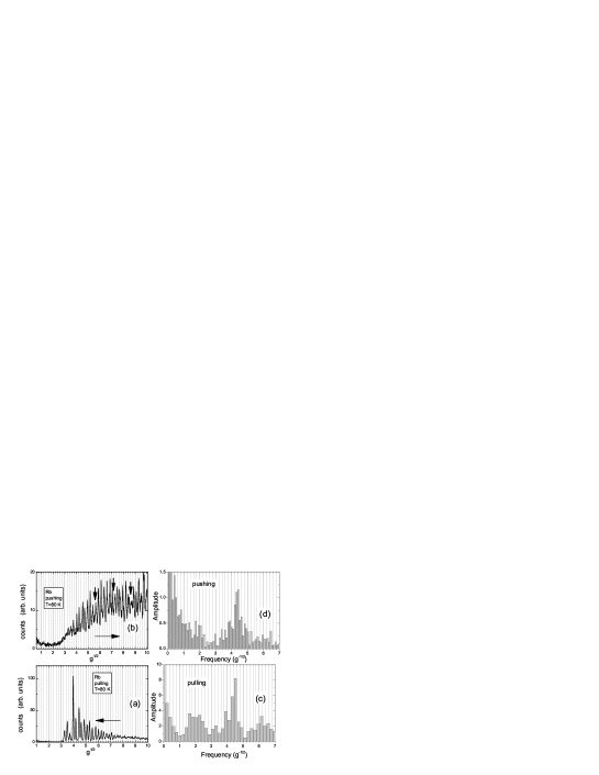
Turning to the conductance histogram (Fig.6 (a)), one notices that at the given temperature the wires with conductances up to are not stable, and for the return histogram (Fig.6 (b)) a clear modulation of the peak amplitudes is visible. The envelope period embraces approximately 6 atomic shell oscillations. As we mentioned in Refs. atomic, and FNT, , the 6-fold period approximately corresponds to a full atomic layer coverage of the hexagonal wire, and each oscillation corresponds to the coverage of a single facet in the hexagonal symmetry of the crystal structure of the neck. Here, again we can see an example that the forward and reverse histograms differ from each other.
It is interesting that further measurements at K the nanowires revert to the electronic shell effect in the regular (pulling) histogram with some retardation in time of about 15 minutes, during which the metal might be purified by continuous cycling Untiedt . This reappearance concerns only the forward (stretching) histograms, while for the backward (compressing) movement no stable nanowire appears up to conductances .
It is important to realize how the nanowire behaves during recording of the scan cycles (forward-return cycles). In reality, most of the stretching scans do not survive down to conductances . Instead, they show a break at larger conductances. Atoms migrate from the protrusions left on the banks after breaking to the bulk of the electrodes until the reverse movement of break-junction electrodes recovers the electrical contact. A gap (expressed as Volts applied to the piezo driver of the controllable break-junction) appears between the end of the pulling and the onset of the pushing movement (see, for example, Figs.7, 8, and 9). This gap becomes larger the higher the mobility of the atoms at given experimental conditions (temperature, adsorbates on the surface). In the case where the electronic shell structure reappears the gap becomes much larger than that for the scans of atomic shell structure recorded at lower temperatures. This implies that the reversed reappearance of the electronic shell structure corresponds to faster atomic mobility, possibly close to the liquid state for the surface atoms. Finally, if we decrease the temperature once again (say, from 80 to 60 K), the atomic shell structure is recovered.
IV Cesium: scans and histograms
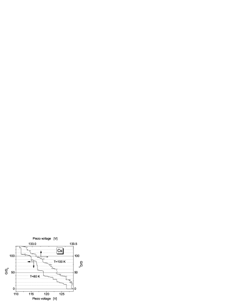
Rb and Cs are very similar in their properties. All the features that we ascribe to Rb can also be found in Cs nanowires and vice versa. In this section we would like to show how scans of the Cs break junctions evolve with temperature along with the histograms. The characteristics of the Cs nanowire at K are shown in Fig.7.


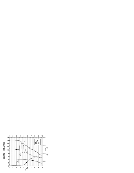
The directions of recording are shown with arrows superimposed on the data curves. The stretching wire corresponds to an increase in the piezo voltage. One can see a hysteresis in the forward and backward directions, and a gap of about 0.5 V, due to retractions of atoms to the electrodes while the contact breaks. Although an accurate calibration has not been attempted and varied in different experiments, for the same series the change in Vpiezo scale induced by the temperature is quite certain. The histogram is constructed from several thousands scans, which vary widely and one of them is shown by the dotted curve in Fig.7. As a whole, they produce a reproducible histogram shown in the same graph. Some of the strongest peaks in the forward direction (at , 3) are seen in the scan as a steeper part, but most of the steps do not correspond to any feature in the histograms. This means that these steps are completely random and give a monotonous background seen at high () conductances.
For this particular junction, an increase in temperature up to 70 K transforms the shell structure to the atomic one (Fig.8).
There is no immediate agreement between the steps in the scans to any of the extrema in the atomic-structure part of the histogram. Electronic shell structure is observed at , 3.4, 3.8 and corresponding steps are seen in the stretching scan. At a still higher temperatures (80 K, Fig.9), the electronic shell oscillations reappear (as in the case with Rb) with a noticeable increase of the gap in the piezo voltage between forward and return scans. We recall that the scans shown are representative of many different scans used to built the histogram.
The most spectacular series of temperature dependent histograms for Cs is shown in Fig.10.
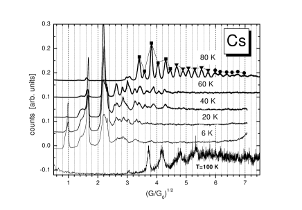
It demonstrates an example of how the low temperature electronic oscillations gradually transform to the atomic ones, starting already at rather low temperatures. At K the atomic oscillations prevail and are clearly grouped by sixes, shown with different symbols on top of each of the maxima. At a still higher temperatures (100 K) the histogram shows the above mentioned reversed transformation to the electronic shell structure. We suggest that the wire becomes fully liquid. More precisely, the speed of surface diffusion of the atoms becomes much faster than the experimental timescale. This suggestion is justified by the corresponding scans (Fig.11), which confirm that at K the neck is solid because of the well defined step structure, while at K such a dependence becomes noisy and destroyed.
Note, also, the dramatic shrinking of the length of stretching of the wire, which in the solid state amounts about 12 V on the piezovolt scale, while in the liquid state (100 K) this is only 0.5 V.
Fig.10 presents an example of how at low temperatures (20 K) the atomic shell oscillations for heavy alkali are superimposed on the electronic ones. In part, this is due to the heavy atomic weight since we never observed such a transition in the lightest metal, Li. In cluster physics, the transition between electronic and atomic shells is connected to the cooling of the cluster beam. It is believed that electronic shell structure is observed in the liquid state of a cluster, while the atomic structure corresponds to the solidification of the metal cluster. In nanowires in most cases we deal with solid necks since the step-like scans conclusively persuade us of the succession of elastic elongation and yielding stages. The latter is impossible in the liquid state. The higher temperatures greatly enhance the thermal fluctuations of the atoms forcing them to explore many locations, some of which may have a lower total free energy due to minima in the electronic contribution. Energy which is released during yielding may cause further heating. Upon rearrangement the atoms on average fall into the deepest free energy minimum, where the shell structure plays a noticeable role.
V Summary
We supplement our previous study of light alkali metals Li, Na, and K with heavy alkalis Rb and Cs. All the features discovered in that study were observed here. Besides, some additional observations confirming our previous results were obtained.
The low-temperature conductance quantization features for the smallest cross-sections are the same for all five alkalis studied. There exist some differences in relative intensities of the peaks near 5, and 6 between the conductance histograms of different metals, in particular for the peak near 5. We explain the enhancement of the latter peak for heavy alkalis by the electronic shell effect extending to lower radii due to a lower melting point.
The evolution of conductance histograms and their Fourier spectra with rising temperature, showing the transition to atomic (geometric) shell oscillations, exhibits the fundamental frequency 4.5 . For heavy alkalis the atomic shells are observed at lower temperatures than for the lighter ones, due to their lower melting point.
One of the unexpected observation is the reverse transitions from the atomic shell structure to the electronic one with rising temperature. We explain this by relative heating of heavy alkali metal nanowire having lower melting point.
References
- (1) B.J. van Wees, H. van Houten H., C.W.J. Beenakker, J.G. Williamson, L.P. Kouwenhoven, D. van der Marel, and C.T. Foxon. Phys. Rev. Lett. 60, 848 (1988).
- (2) J.M. Krans, C.J. Muller, I.K. Yanson, Th.C.M. Govaert, R. Hesper, and J.M. van Ruitenbeek. Phys. Rev. B 48, 14721 (1993).
- (3) W.D. Knight, K. Clemenger, W.A. de Heer, W.A. Saunders, M.Y. Chou, and M.L. Cohen. Phys. Rev. Lett. 52, 2141 (1984); W.A. de Heer, Rev. Mod. Phys. 65, 677 (1993)
- (4) A.I. Yanson, I.K. Yanson, and J.M. van Ruitenbeek, Nature (London) 400, 1440 (1999).
- (5) T.P. Martin. Phys. Rep. 273, 199 (1996).
- (6) A.I. Yanson, I.K. Yanson and J.M. van Ruitenbeek, Phys. Rev. Letters 87, 216805 (2001).
- (7) A.I. Yanson, I.K. Yanson, and J.M. van Ruitenbeek, Fiz. Nizk. Temp. 27, 1092 (2001); Low Temp. Phys. 27, 807 (2001).
- (8) A.I. Yanson, I.K. Yanson, and J.M. van Ruitenbeek, Phys. Rev. Lett. 84, 5832 (2000).
- (9) J.A. Torres and J.J. Saenz, Phys. Rev. Lett. 77, 2245 (1996).
- (10) B. Ludoph, M.H. Devoret, D. Esteve, C. Urbina, and J.M. van Ruitenbeek. Phys. Rev. Lett. 82, 1530 (1999).
- (11) C. Untiedt, G. Rubio, S. Vieira, and N. Agraït, Phys. Rev. B 56, 2154 (1997).