]Present address: Physics Department, Harvard University, Cambridge, MA 02138
Spin-dependent transport in molecular tunnel junctions
Abstract
We present measurements of magnetic tunnel junctions made using a self-assembled-monolayer molecular barrier. Ni/octanethiol/Ni samples were fabricated in a nanopore geometry. The devices exhibit significant changes in resistance as the angle between the magnetic moments in the two electrodes is varied, demonstrating that low-energy electrons can traverse the molecular barrier while maintaining spin coherence. An analysis of the voltage and temperature dependence of the data suggests that the spin-coherent transport signals can be degraded by localized states in the molecular barriers.
pacs:
85.30.Mn, 85.65.+h, 85.75.-dThe field of molecular electronics has made a number of recent advances, with measurements performed on single molecules, and demonstrations that molecules can exhibit diode and transistor behaviors Reed ; Kergueris ; Weber ; Metzger ; Zhou_APL_97 ; Park ; Liang ; Nitzan . However, to date nearly all molecular-electronics experiments have focused on charge transport, without taking advantage of the electron’s spin. Exceptions are experiments on carbon nanotubes contacted by ferromagnetic electrodes Tsukagoshi_Nature_99 and spin transport of photo-excited ( 1 eV) carriers through organic linkers between semiconductor quantum dots Awschalom_Science_03 . Molecular devices may be well-suited for applications requiring spin manipulation because the relative weakness of spin-orbit and hyperfine interactions in many molecules, compared to conventional semiconductor systems, may help to isolate the spin from external degrees of freedom. Here we study the spin-polarized transport of electrons tunneling through a barrier consisting of a self-assembled organic monolayer between two magnetic electrodes. We find that spin coherence can be maintained during the tunneling process, as demonstrated by changes in resistance as we vary the relative orientations of the magnetic moments in the two electrodes. Our measurements demonstrate that spin-coherent transport in molecular devices is possible for low-energy electrons, as distinct from previous demonstrations for photo-excited carriers Awschalom_Science_03 . However, our molecular barriers are not ideal. Strong voltage and temperature dependence of the junction magnetoresistance (JMR) and time-dependent telegraph-noise signals suggest that the device properties can be affected by localized states in the molecular barriers.
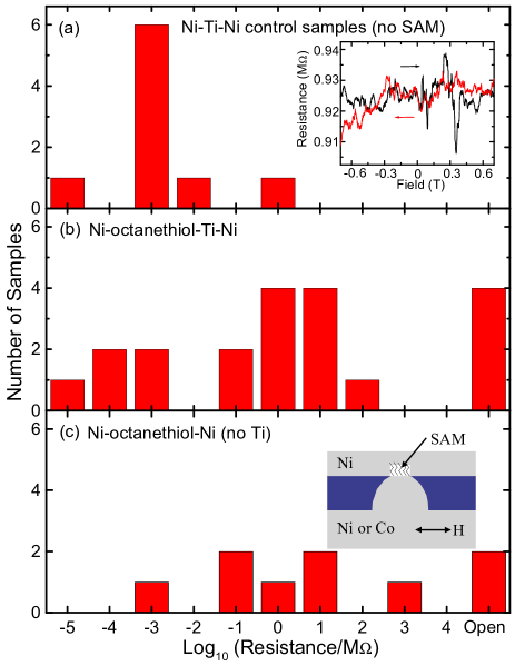
We fabricate nanometer-scale tunnel junctions with self-assembled molecular barriers using the nanopore technique Ralls_APL_89 , employed previously to study conduction through molecular layers in nonmagnetic tunnel junctions Zhou_APL_97 ; Petta_APL_00 ; Wang . First, we use electron-beam lithography and a timed reactive-ion etch to fabricate a bowl-shaped hole through a suspended silicon-nitride membrane. The area of the holes is characterized by evaporating Cu onto both sides of test samples without breaking vacuum, measuring the resistance of the metal contacts formed through individual holes, and estimating the area of the contact using the Sharvin formula, Sharvin . We find hole diameters in the range of 5–10 nm. Once a set of holes is made, the procedure to create the molecular tunnel junctions begins by evaporating a 10 Å Ti adhesion layer (which does not fill the hole), followed by 1000 Å of Ni and 500 Å of Cu onto the bowl-shaped side of the sample (the bottom side of the schematic in the inset of Fig. 1(c)). After breaking vacuum, we immerse the samples immediately in a 1 mM solution of octanethiol in ethanol, transfer them to an Ar glove box, and leave them to react for at least 48 hours to form a self-assembled monolayer (SAM) of octanethiol on the Ni Mekhalif_Langmuir_03 . We choose to use octanethiol because the transport properties of this molecule in contact with non-magnetic electrodes have been studied extensively Bumm ; Wold ; Cui ; Wang . Before evaporation of the top contact, we rinse the samples with ethanol and blow dry with dry N2. The samples are then transferred to an evaporator and pumped to high vacuum (10-7 Torr). For most of the devices described below we deposit 10 Å of Ti, followed by 300 Å of Ni or Co and a 1000 Å Cu capping layer. Because the Ti adhesion layer could damage the organic monolayer, we have also fabricated samples without any Ti in the top contact near the sample region. Devices fabricated with and without Ti had similar magnetoresistance curves. All top-contact evaporations are performed at a low rate (0.1–0.2 Å/s) and with the target cooled to 77 K to minimize damage to the molecular layer. By convention, positive voltages () correspond to electron flow from bottom to top in the device schematic in Fig. 1(c). Unless specified otherwise, all transport measurements were taken at a temperature of 4.2 K.
To characterize our monolayers, as well as to distinguish effects due merely to the solvent or the processing procedures, rather than the SAM, we fabricated control samples by immersing the devices in pure ethanol solvent for 48 hours instead of octanethiol solution. For both the control samples and the SAM devices, we found a distribution of resistance values (Fig. 1). All but one of 9 controls without octanethiols had resistances below 25.8 k, indicating the presence of a metallic contact Warning . Several of the SAM samples also had low resistances, from which we infer the presence of metallic shorts through the molecular layer. However, 23 of 29 octanethiol devices had resistances greater than , indicating electron transport via a tunneling mechanism. The resistance values clustered in the M range are similar to previous measurements of alkanethiol molecules using Au electrodes in a nanopore geometry Wang . In the following, we will focus solely on the junctions with resistance greater than .
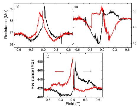
In Fig. 2(a–c) we plot the resistance (), measured at 4.2 K, as a function of magnetic field () applied in the sample plane for three Ni-octanethiol-Ti-Ni samples with varying resistances. For 0.6 T, the magnetizations of the two electrodes are parallel, resulting in an -independent resistance . We note that the saturation field is larger than for simple planar Ni films, presumably due to the bowl-shaped contact on one side of the device (inset, Fig. 1(c)). As is swept through zero, the magnetizations of the two electrodes undergo reversal processes at different fields, so that they may approach an approximately antiparallel configuration before ultimately aligning with the reversed field. During this process, the samples exhibit clear changes in resistance, reaching values of that are generally higher than , although in some samples for a range of the resistance may also dip below (e.g., Fig. 2(a–b)). If is the maximum resistance measured and is the minimum, we define the positive and negative junction magnetoresistances (-)/ and (-)/. For the three samples in Fig. 2 we find 3.5%, -6.1%, and 16.0% for (a–c), respectively (see figure caption for bias voltages). In comparison, the low resistance Ni-ethanol-Ti-Ni control samples with no octanethiol barriers exhibited much smaller resistance changes and qualitatively different magnetoresistance traces (see the inset of Fig. 1(a)).
An estimate for the value of JMR corresponding to the mechanism of direct electron tunneling through a barrier is given by the Julliere formula, JMR = 2/(1-), where and are the tunneling spin polarizations associated with the two electrodes Julliere_PLA_75 . For Ni, where 0.31, the Julliere estimate is JMR = 21% Monsma . The largest JMR that we have measured is 16%, for a bias voltage of 5 mV (Fig. 2(c)). This is 3/4 of the Julliere value, from which we conclude that the electron spin is capable of maintaining a high degree of coherence during the tunneling process.
The measured values of JMR are strongly correlated with the sample resistance, with the largest magnitudes associated with the most resistive samples (Fig. 3(a)). This suggests that imperfections in the SAM, which should lower , can also reduce the JMR. The smaller JMR values are likely due to contributions from transport mechanisms that differ from simple direct tunneling through the molecular barrier, as discussed below.
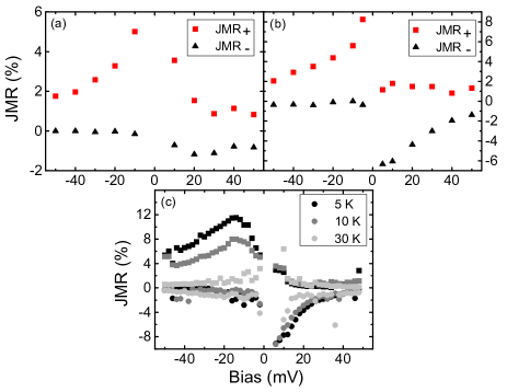
The quality of the SAM tunnel barriers can be characterized in more detail by measurements of the voltage and temperature dependence of their transport properties. In Fig. 3(b), we plot a high bias - curve from a high-resistance Ni-octanethiol-Ti-Ni junction as a function of , along with a fit to the Simmons tunneling model Wang ; Simmons . The fit suggests a barrier height of 1.510.02 eV, in rough agreement with the value of 1.4 eV measured for alkanethiols on gold Wang . We illustrate the and dependence of the JMR in figures 4 and 5. The magnitude of the JMR depends strongly on in all samples, and for some devices the JMR can change sign to produce negative values in particular ranges of and . In all samples, the magnitude of the JMR decreases for large enough values of , and is typically reduced to less than 2% for 40 mV (Fig. 4). The magnetoresistance is strongly temperature dependent, as well (Fig. 4(c)).
Previously, qualitatively similar and dependences have been observed for oxide tunnel barriers, for which the characteristic voltage scale of the decaying magnetoresistance can vary from 3 mV to 500 mV, depending on the barrier quality Tsymbal_review . For oxide barriers, the mechanisms behind negative JMR values and the and dependence of magnetoresistance have been controversial, but the recent observation that vacuum tunnel barriers give magnetoresistances with very little dependence Wulfhekel provides evidence that two-step tunneling through localized states in the tunnel barrier is a possible explanation for all three effects Zhang_JAP ; Tsymbal_PRL ; Tsymbal_review . We suggest that, in a similar way, localized states in the octanethiol barrier may explain many of the anomalous features that we measure as a function of and .

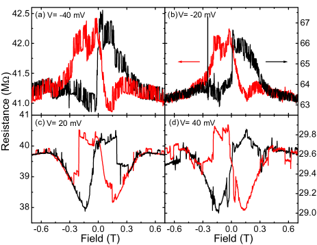
Several of our samples exhibit striking time-dependent two-level resistance fluctuations, i.e. telegraph noise (Fig. 5). The frequency of the fluctuations varies as a function of both and Xiao . The fluctuations could be due either to the motion of electrons within localized charge defects or to changes in the structural properties of the junctions. In either case, they demonstrate the importance of imperfections in the molecular barrier. The size of the changes in resistance suggest that a very small number of molecules may be involved in these fluctuations. For example, in sample #2, the resistance at =0 fluctuates by 0.5 M out of a total resistance of 42 M at =-40 mV (see Fig. 5), for a fractional fluctuation of 0.01. We estimate that the device area is in the range 20–80 nm2, based on the Sharvin resistance of test nanopores filled with Cu. Assuming a packing density of molecules/nm2 Widrig , the device should therefore contain 100–400 molecules. A fractional change of 0.01 therefore corresponds to having 1–4 molecules switch their conductance between fully off and on states, using the very rough assumption that all molecules contribute equally to transport. In other devices, the amplitude of the telegraph signals corresponds to fluctuations by a conductance equivalent to 1–12 molecules. These numbers should be considered upper bounds, because if transport through the barriers is non-uniform then the relative strength of signals from individual molecules could be enhanced.
In conclusion, we have fabricated and measured the transport properties of magnetic tunnel junctions containing octanethiol tunnel barriers. We find, first, that spin coherence can be maintained in transport through these molecular devices. The tunnel junctions exhibit JMR values of up to 16% at low bias voltages. This suggests that molecular bridges may prove useful in applications involving electron-spin manipulation. However, we also find a correlation between the JMR and the sample resistances, strong and dependence for the magnetoresistance, negative JMR values for particular ranges of and in some samples, and the presence of telegraph noise. All of these factors suggest the presence of localized states within the octanethiol barrier Zhang_JAP ; Tsymbal_PRL ; Tsymbal_review . The origin of these states is uncertain. They could be formed in the physical process of top-layer deposition, by chemical reactions between the monolayer and the metals, or by stress Son . A better understanding of the growth of SAMs on magnetic surfaces and improved procedures for depositing top contacts are likely to improve device yield and increase the JMR.
Acknowledgements.
We thank R. A. Buhrman for discussions. This work was supported by DARPA (N00173-03-1-G011), the ARO (DAAD19-01-1-0541), and the NSF (DMR-0244713). A portion of the work was performed at the NSF-funded Cornell Nanoscale Facility/NNIN.References
- (1) M. A. Reed, C. Zhou, C. J. Miller, T. P. Burgin, and J. M. Tour, Science , 252 (1997).
- (2) C. Kergueris et al., Phys. Rev. B , 12505 (1999).
- (3) H. B. Weber et al., Chem. Phys. , 113 (2002).
- (4) R. M. Metzger et al., J. Am. Chem. Soc. , 10455 (1997).
- (5) C. Zhou, M. R. Deshpande, M. A. Reed, L. Jones II, and J. M. Tour, Appl. Phys. Lett. , 611 (1997).
- (6) J. Park et al., Nature , 722 (2002).
- (7) W. J. Liang et al., Nature , 725 (2002).
- (8) A. Nitzan and M. A. Ratner, Science , 1384 (2003) and references therein.
- (9) K. Tsukagoshi, B. W. Alphenaar, and H. Ago, Nature , 572 (1999).
- (10) M. Ouyang and D. D. Awschalom, Science , 1074 (2003).
- (11) K. S. Ralls, R. A. Buhrman, and R. C. Tiberio, Appl. Phys. Lett. , 2459 (1989).
- (12) W. Wang, T. Lee, and M. A. Reed, Phys. Rev. B , 035416 (2003).
- (13) J. R. Petta, D. G. Salinas, D. C. Ralph, Appl. Phys. Lett. , 4419 (2000).
- (14) A. G. M. Jansen, A. P. van Gelder, and P. Wyder, J. Phys. C, , 6073 (1980).
- (15) Z. Mekhalif, F. Laffineur, N. Couturier, and J. Delhalle, Langmuir , 637 (2003).
- (16) L. A. Bumm, J. J. Arnold, T. D. Dunbar, D. L. Allara, and P. S. Weiss, J. Phys. Chem. B , 8122 (1999).
- (17) D. J. Wold and C. D. Frisbie, J. Am. Chem. Soc. , 5549 (2001).
- (18) X. D. Cui et al., Nanotechnology , 5 (2002).
- (19) It is important to use ethanol as the solvent. Other control samples made using THF as the solvent exhibit resistances in the M range in the absence of any SAM, indicating the formation of an insulating surface layer.
- (20) M. Julliere, Phys. Lett. A, , 225 (1975).
- (21) D. J. Monsma and S. P. P. Parkin, Appl. Phys. Lett. , 720 (2000).
- (22) J. G. Simmons, J. Appl. Phys. , 1793 (1963).
- (23) E. Y. Tsymbal, O. N. Mryasov, and P. R. LeClair, J. Phys.:Condens. Matter , R109 (2003).
- (24) W. Wulfhekel, H. F. Ding, and J. Kirschner, J. Magn. Magn. Mater. , 47 (2002).
- (25) J. Zhang and R. M. White, J. Appl. Phys. , 6512 (1998).
- (26) E. Y. Tsymbal, A. Sokolov, I. F. Sabirianov, and B. Doudin, Phys. Rev. Lett. , 186602 (2003).
- (27) M. Xiao, I. Martin, and H. W. Jiang, Phys. Rev. Lett. , 078301 (2003).
- (28) C. A. Widrig, C. A. Alves, and M. D. Porter, J. Am. Chem. Soc. , 2805 (1991).
- (29) K.-A. Son, H. I. Kim, and J. E. Houston, Phys. Rev. Lett. , 5357 (2001).