Computing with spins: From classical to quantum computing
Abstract
This article reviews the use of single electron spins to compute. In classical computing schemes, a binary bit is represented by the spin polarization of a single electron confined in a quantum dot. If a weak magnetic field is present, the spin orientation becomes a binary variable which can encode logic 0 and logic 1. Coherent superposition of these two polarizations represent a qubit. By engineering the exchange interaction between closely spaced spins in neighboring quantum dots, it is possible to implement either classical or quantum logic gates.
1 Introduction
The visionary who first thought of using the spin polarization of a single electron to encode a binary bit of information has never been identified conclusively. Folklore has it that Feynman mentioned this notion in casual conversations (circa 1985), but to this author’s knowledge there did not exist concrete schemes for implementing spintronic logic gates till the mid 1990s. Encoding information in spin may have certain advantages. First, there is the possibility of lower power dissipation in switching logic gates. In charge based devices, such as metal oxide semiconductor field effect transistors, switching between logic 0 and logic 1 is accomplished by moving charges into and out of the transistor channel. Motion of charges is induced by creating a potential gradient (or electric field). The associated potential energy is ultimately dissipated as heat and irretrievably lost. In the case of spin, we do not have to move charges. In order to switch a bit from 0 to 1, or vice versa, we merely have to toggle the spin. This may require much less energy. Second, spin does not couple easily to stray electric fields (unless there is strong spin-orbit interaction in the host material). Therefore, spin is likely to be relatively immune to noise. Finally, it is possible that spin devices may be faster. If we do not have to move electrons around, we will not be limited by the transit time of charges. Instead, we will be limited by the spin flip time, which could be smaller.
2 Spintronic classical (irreversible) logic
In 1994, we proposed a concrete scheme for realizing a classical universal logic gate (NAND) using three spins placed in a weak magnetic field [1]. By “three spins”, we mean the spin orientations of three conduction band electrons, each confined in a semiconductor quantum dot. The system is shown schematically in Fig. 1. Exchange interaction is allowed only between nearest neighbor spins (second nearest neighbor interaction is considered too weak to have any effect). Because of the magnetic field, the spin orientation in any quantum dot becomes a binary variable. The spin polarization is either along the magnetic field, or opposite to the field. To understand this, consider the Hamiltonian of an isolated dot:
| (1) |
where is the unperturbed Hamiltonian in the absence of the magnetic field, is the magnetic field, is the Landé g-factor of the quantum dot material, is the Bohr magneton, and is the Pauli spin matrix. If the magnetic field is directed along the z-direction, then
| (2) |
Diagonalizing the above Hamiltonian yields the eigenspinors (1,0) and (0,1) which are +z– and -z–polarized spins. Therefore, the spin orientation is a binary variable; it is either parallel or anti-parallel to the applied magnetic field.

In the presence of exchange interaction between two electrons confined to two separate potentials (such as two different quantum dots), the anti-ferromagnetic ordering, or the singlet state, (i.e. two neighboring spins are anti-parallel) is preferred over the ferromagnetic ordering, or triplet state (two spins are parallel) [2]. We will assume that the tendency to preserve this anti-ferromagnetic ordering is stronger than the tendency for all spins to line up along the magnetic field. This merely requires that the exchange splitting energy (energy difference between triplet and singlet states) exceed the Zeeman splitting energy . We ensure this by reducing the potential barrier between neighboring dots to enhance the exchange, while at the same time, making the magnetic field sufficiently weak to reduce the Zeeman energy. Under this scenario, the ground state of the array has the spin configuration shown in Fig. 1(a). We will call “upspin” the spin orientation directed along the magnetic field and “downspin” the opposite orientation.
We encode logic 1 in the upspin state. Furthermore, we will consider the two edge dots in Fig. 1(a) as input ports to a logic gate, and the middle dot as the output port. It is obvious that when the two inputs are logic 1, the output will be logic 0 when the system reaches ground state (anti-ferromagnetic ordering).
Next, consider the situation when the two inputs are logic 0 (see Fig. 1(b)). The output must be logic 1 in order to conform to the anti-ferromagnetic ordering. However, there is a subtle issue. Fig. 1(b) is actually not the ground state of the system, Fig. 1(a) is. This is because of the weak magnetic field. The difference between Fig. 1(a) and Fig. 1(b) is that in the former case, two spins are aligned parallel to the magnetic field, while in the latter, two spins are aligned anti-parallel to the magnetic field. Therefore, if the system is left in the state of Fig. 1(b), it must ultimately decay to the state in Fig. 1(a), according to the laws of thermodynamics. But that may take a very long time because of three reasons. First, the system must emit some energy carrying entity to decay. This entity is most likely a phonon. However, phonon emissions in quantum dots are suppressed by the “phonon bottleneck” effect [3]. Second, phonons do not couple easily to spin unless we have a strongly pyroelectric material as the host. Finally, if spins flip one at a time (all three spins flipping simultaneously is very unlikely), then in order to access the state in Fig 1(a), the state in Fig. 1(b) will have to go through a state where two neighboring spins will be parallel. Such a state is much higher in energy than either Fig. 1(a) or Fig. 1(b). Therefore, Fig. 1(a) and Fig. 1(b) are separated by an energy barrier, making Fig. 1(b) a long lived metastable state. As long as the input bit rate is high enough so that inputs change much more rapidly than the time it takes for the metastable state to decay to the global ground state of Fig. 1(a), we need not worry about this issue.
What happens if one of the inputs is logic 1, and the other is logic 0 as shown in Fig. 1(c)? Here the magnetic field comes in handy to break the tie. In this case, logic 1 is preferred as the output since the all other things being equal, a spin would prefer to line up parallel to the magnetic field, rather than anti-parallel. Thus, when either input is logic 0, the ouput is logic 1. We have realized the truth table in Table 1.
| Input 1 | Input 2 | Output |
| 1 | 1 | 0 |
| 1 | 0 | 1 |
| 0 | 1 | 1 |
| 0 | 0 | 1 |
The reader will recognize that this is the truth table of a NAND gate, which is one of two universal Boolean logic gates. Since we can realize a NAND, we can realize any arbitrary Boolean logic circuit (combinational or sequential) by connecting NAND gates. A number of different logic devices (half adders, flip-flops, etc.) were designed and illustrated in ref. [1].
These devices have been extensively studied by others [4, 5] using time independent simulations. The time-independent simulations address the steady state behaviors and therefore do not directly reveal a serious problem with these devices that was already recognized in ref. [1]. In the following section, we explain this problem.
3 Problem: Lack of unidirectionality
At the time these logic gates were proposed, it was also realized that they have a severe shortcoming that precludes their use in pipelined architectures [1]. To understand the nature of the problem, consider three inverters (NOT gates) in series. A single NOT gate is the simplest device; it is realized by two exchange coupled spins, one of which is the input and the other is the output. Because of the anti-ferromagnetic ordering, the output is always the logic complement of the input.

Fig. 2(a) shows three conventional inverters in series and Fig. 2(b) shows the corresponding spintronic realization. The input to the first inverter is logic 1 and the output of the last inverter is logic 0, as it should be. But now, let us suddenly change the input at the first inverter to logic 0 at time = 0. The situation at time = 0+ is shown in Fig. 2(c). We expect that ultimately the output of the last inverter will become logic 1. Unfortunately, this cannot happen. In Fig. 2(c), the second spin from the left finds its left neighbor asking it to flip (because of the exchange interaction that enforces anti-ferromagnetic ordering between two neighboring spins) while its right neighbor is asking it to stay put because of the same exchange interaction. Both influences – from the left and from the right – are exactly equally strong and the second cell is stuck in a logic indeterminate state that it cannot get out of [6]. Rolf Landauer later termed it a metastable state that prevents decay to the desired ground state [7]. In fact, if we take the external magnetic field into account, then there is a preference for the second cell to actually not flip in response to the input since there is a slight preference for the upspin state because of the external magnetic field. In this case, the logic signal cannot propagate from the input to the output and the circuit simply does not work! Similar situations were examined in ref. [8]. The real problem is that exchange interaction is bidirectional which cannot ensure unidirectional flow of logic signal from the input to the output of the logic device. This unidirectionality is a required attribute of any logic device (for the five necessary requirements of a classical logic device, see ref. [9]). We can think of desperate measures to enforce the unidirectionality. For example, we can claim that if we hold the input at the first inverter (leftmost cell in Fig. 2(c)) to logic 0, and do not let go, then the second cell which is equally likely to follow its left neighbor and right neighbor, will have no option but to ultimately follow its left neighbor since it is adamant and persistent (we are not letting go of the input). This will happen in spite of the magnetic field since the exchange energy is larger than the Zeeman splitting. In this case, we are trying to enforce unidirectionality via the input signal itself (note that the input device does indeed break the inversion symmetry of the system in Fig. 2(c)). This possible remedy was studied theoretically in ref. [10] which reached the conclusion that it does not always work. In fact, the process of logic signal propagation under this scenario is inefficient thermally assisted random walk and the final logic state, if reached, can be destroyed by thermal fluctuations. The idea of using the input device to enforce unidirectionality was also implicitly used in the experiment of ref. [11]. While this may work for a few cells (as it did in ref. [11]), it will obviously not work for a large number of cells since the influence of the input decays with increasing distance from the input. Ultimately, the remote cells that are far from the input, will not feel the input’s effect and remain stuck in metastable states, producing wrong answers to simple logic problems.
3.1 Possible solution
In ref. [1], one solution that was offered to break this impasse was to progressively increase the distance between cells. This makes the influence of the left neighbor always stronger than that of the right neighbor since the strength of the exchange interaction has an exponential dependence on the separation between neighboring cells. This is not an elegant solution since ultimately the exchange splitting energy will become smaller than the Zeeman splitting energy, at which point the paradigm will no longer work.
In 1996, we proposed a more elegant solution [12]. This was inspired by the realization that in charge coupled device (CCD) arrays, there is no inherent unidirectionality, yet charge is made to propagate from one device to the next unidirectionally. This is achieved by clocking. We mentioned that unidirectionality can be imposed in time or space [12] and clocking imposes unidirectionality in time. However, a cursory examination revealed that normal clocking will not work in our case. Say, we put gate pads on the barriers between neighboring cells. Initially, all the the barriers are high and opaque so that there is no overlap between the wavefunctions of adjacent electrons and hence no exchange interaction between neighboring spins. Now, we lower the first barrier by applying a positive potential to gate 1 as shown in Fig. 2(d). This allows the wavefunctions of electrons on either side of the gate pad to leak out into the barrier, overlap. and cause an exchange interaction. Exchange causes the second spin to assume a polarization anti-parallel to the input spin orientation since the singlet state is lower in energy than the triplet. In other words, the second cell switches. At this point, if we let go of the input, raise the first barrier back up, and lower the second barrier by applying a positive potential to gate 2, then either the third cell switches in response to the second (which is shown in the upper branch), or the second cell switches in response to the third (which is shown in the lower branch). The upper branch is the desired state, but it is equally likely that the lower branch will result since both branches obey the ant-ferromagnetic ordering between the two exchange coupled cells (cell 2 and 3). Therefore, a simple sequential clock will not work. What is required is that both gate 1 and gate 2 have positive potentials while the input is applied. Now the first three cells assume the correct polarizations as shown in Fig. 2(e). Then, the input is removed, gate 1 is returned to zero potential and positive potentials are applied to gates 2 and 3. This causes the first four cells to assume the correct polarization, and so on. This situation is shown in Fig. 2(f) and is the desired configuration. Thus by lowering two adjacent barriers pairwise at the same time, we can propagate the input state through a linear array. In other words, we will need a three-phase clock, a single phase will not work. The three clock pulse trains for a three-phase clock are shown in Fig. 2(g). Each train is phase shifted from the previous one by radians. Such a situation is not unusual since charge coupled device arrays also need a multi-phase clock (push clock, drop clock) to work [13].
While, multi-phase clocking can make these devices work, it is hardly an attractive solution since one needs to fabricate gate pads between every two cells. The separation between the cells may need to be 5 nm in order to have sufficient exchange coupling. Aligning a gate pad to within a space of 5 nm is a major lithography challenge. Furthermore, the gate potentials are lowered and raised by moving charges into and out of the gate pads, leading to considerable energy dissipation that completely negates the advantage of using spins. Therefore, these devices present interesting physics, but at this time, do not appear to be serious candidates for practical applications.
4 Using spin as a qubit
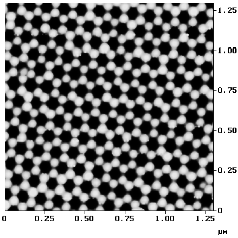
So far, we have discussed the use of spin in classical irreversible logic gates. These logic gates dissipate a minimum of amount of energy per bit flip [14]. Let us assume that we can make quantum dots with a density of 1012 cm-2. Quantum dots self assembled by electrochemical techniques in our own lab (and in many other labs) can achieve this density today. We show a raw atomic force micrograph of quantum dots self assembled in our lab in Fig. 3. The dark areas are the dots and the surrounding light areas are the barriers. The dot diameter in this micrograph is 50 nm and the dot density is close to 1011 cm-2. By using slightly different synthesis conditions, we can actually achieve densities exceeding 1012 cm-2.
Let us now assume that we can flip the spin in a quantum dot in 1 psec. Then the minimum power that will be dissipated per unit area will exceed /(1 psec) = 3 kW/cm2 (actually most of the power will be dissipated in the clock cycles, which we have ignored). This dissipation is at least 30 times more than what the Pentium IV chip dissipates [15]. Although removal of 1 kW/cm2 of heat from a chip was demonstrated almost two decades ago, removing 3 kW/cm2 from a chip is still a major challenge in heat sinking.
The obvious way to overcome (or, rather, circumvent) this challenge is to develop reversible logic gates that are not constrained by the Landauer barrier. In 1996, we devised a logically and physically reversible quantum inverter using two exchange coupled spins [16]. This device is very similar to the single electron parametron idea [17] and can be viewed as a single spin parametron. Since either spin could exist in a coherent superposition of two orthogonal spin states (call them “upspin” and “downspin” states), this would also be a “qubit”. Later, Loss and DiVincenzo devised a universal quantum gate using two exchange coupled spins in two closely spaced quantum dots [18]. Recently, experimental demonstration of coherent transfer of electron spins between quantum dots coupled by conjugated molecules has been demonstrated, opening up real possibilities in this area [19].
5 Spintronic quantum gates
The idea of using a single electron or nuclear spin to encode a qubit and then utilizing this to realize a universal quantum gate, has taken hold [20, 21, 18, 22]. The motivation for this is the realization that spin coherence times in solids is much larger than charge coherence time. Charge coherence times in semiconductors tend to saturate to about 1 nsec as the temperature is lowered [23]. This is presumably due to coupling to zero point motion of phonons which cannot be eliminated by lowering temperature [23]. On the other hand, electron spin coherence times of 100 nsec in GaAs at 5 K has already been reported [24] and much higher coherence times are expected for nuclear spins in silicon [25]. Therefore, spin is obviously the preferred vehicle to encode qubits in solids. Using spin to carry out all optical quantum computing has also appeared as a viable and intriguing idea [26]. The advantage of the all-optical scheme over the electronic scheme is that we do not have to read single electron spins electrically to read a qubit. Electrical read out is extremely difficult [32], although some schemes have been proposed for this purpose [27, 28, 29]. Recently, some experimental progress has been made in this direction [30], but reading a single qubit in the solid state still remains elusive,. The difficult part is that electrical read out requires making contacts to individual quantum dots, which is an engineering challenge. In contrast, optical read out does not require contacts. The qubit is read out using a quantum jump technique [31] which requires monitoring the fluorescence from a quantum dot. Recently, it has been verified experimentally that the spin state of an electron in a quantum dot can be read by circularly polarized light [33]. Therefore, optical read out appears to be a more practical approach.
6 Conclusion
In this article we have provided a brief history of the use of single electron spin in computing. We have indicated where and why spin may have an advantage over charge in implementing the type of devices and architectures discussed here.
This work is supported by the US Air Force Office of Scientific Research under grant FA9550-04-1-0261.
References
- [1] S. Bandyopadhyay, B. Das and A. E. Miller, Nanotechnology, Vol. 5, 113 – 133 (1994).
- [2] N. Ashcroft and D. Mermin, Solid State Physics (Saunders College, HRW, 1972).
- [3] H. Benisty, C. M. Sotomayor-Torres, and C. Weisbuch, Phys. Rev. B., Vol. 44, 10945 – 10948 (1991).
- [4] S. N. Molotkov and S. N. Nazin, JETP Lett., Vol. 62, 273 (1995).
- [5] A. M. Bychkov, L. A. Openov and I. A. Semenihin, JETP Lett., Vol. 66, 298 – 303 (1997).
- [6] S. Bandyopadhyay and V. P. Roychowdhury, in Quantum Devices and Circuits, Eds. K. Ismail, S. Bandyopadhyay and J-P Leburton, (Imperial College Press, London, 1997), 271–276.
- [7] R. Landauer, Philos. Trans. R. Soc., Ser. A, Vol. 353, 367– 376 (1995).
- [8] J. C. Lusth, B. Dixon, D. J. Jackson and S. L. Burkett, in Quantum Devices and Circuits, Eds. K. Ismail, S. Bandyopadhyay and J-P Leburton, (Imperial College Press, London, 1997), 289 – 297.
- [9] David A. Hodges and Horace G. Jackson, Analysis and Design of Integrated Circuits, 2nd. edition (McGraw Hill, New York, 1988), Chapter 1, p. 2.
- [10] M. P. Anantram and V. P. Roychowdhury, J. Appl. Phys., Vol. 85, 1622– 1625 (1999).
- [11] R. P. Cowburn and M. E. Welland, Science, Vol. 287, 1466 – 1468 (2000).
- [12] S. Bandyopadhyay and V. P. Roychowdhury, Jpn. J. Appl. Phys., Vol. 35, Part 1, No. 6A, 3350 –3362 (1996).
- [13] D. K. Schröder, Advanced MOS Devices, (Modular Series on Solid State Devices, Vol. VII) Eds. R. F. Pierret and G. W. Neudeck (Addison-Wesley, Reading, Massachusetts, 1989)
- [14] R. W. Keyes and R. Landauer, IBM J. Res. Develop., Vol. 14 , 152 – 157 (1970).
- [15] Suman Datta, Intel Corp., Portland, Oregon, private communication.
- [16] S. Bandyopadhyay and V. P. Roychowdhury, Proceedings of the International Conference on Superlattices and Microstructures, Liege, Belgium, 1996, Also in Superlat. Microstruct., Vol. 22, No. 3, 411–416 (1997).
- [17] K. K. Likharev and A. N. Korotkov, Science, Vol. 273, 763–765 (1996).
- [18] D. Loss and D. P. DiVincenzo, Phys. Rev. A, Vol. 57, 120 – 126 (1998).
- [19] Min Ouyang and David D. Awschalom, Science, Vol. 301, 1074-1078 (2003).
- [20] V. Privman, I. D. Wagner and G. Kventsel, Phys. Lett. A, Vol. 239, 141 – 146 (1998).
- [21] B. E. Kane, Nature (London), Vol. 393, 133 – 137 (1998).
- [22] S. Bandyopadhyay, Phys. Rev. B, Vol. 61, 13813– 13819 (2000).
- [23] P. Mohanty, E. M. Q. Jariwalla and R. A. Webb, Phys. Rev. Lett., Vol. 78, 3366 – 3369 (1997).
- [24] J. M. Kikkawa and D. D. Awschalom, Phys. Rev. Lett., Vol. 80, 4313 – 4316 (1998).
- [25] G. Feher, Phys. Rev., Vol. 114, 1219 (1959).
- [26] T. Calarco, A. Datta, P. Fedichev, E. Pazy and P. Zoller, Phys. Rev. A, Vol. 68, No. 1, 012310-1 – 012310-21 (2003); E. Pazy, E. Biolattia, T. Calarco, I. D’ Amico, P. Zanardi, F. Rossi and P. Zoller, Europhys. Lett., Vol. 62, 175 (2003).
- [27] B. E. Kane, N. S. McAlpine, A. S. Dzurak, R. G. Clark, G. J. Milburn, He Bi Sun and Howard Wiseman, Phys. Rev. B, Vol. 61, 2961 – 2972 (2000).
- [28] Patrick Recher, Eugene V. Sukhorukov and Daniel Loss, Phys. Rev. Lett., Vol. 85, 1962 – 1965 (2000); Hans Andreas Engel and Daniel Loss, Phys. Rev. Lett., Vol. 86, 4648 – 4651 (2001).
- [29] S. Bandyopadhyay, Phys. Rev. B, Vol. 67, 193304-1 – 193304-4 (2003).
- [30] K. Ono, D. G. Austing, Y. Tokura and S. Tarucha, Science, Vol. 297, 1313-1317 (2002).
- [31] A. Imamoglu, Fortschr. Phys. , Vol. 48, 987 (2000).
- [32] H. S. Goan and G. J. Milburn, Phys. Rev. B, Vol. 64, 235307-1 – 235307-12 (2001).
- [33] S. Cortez, et al., Phys. Rev. Lett., Vol. 89, 207401-207404 (2002).