Hopping versus bulk conductivity in transparent oxides: 12CaO7Al2O3
Abstract
First-principles calculations of the mayenite-based oxide, [Ca12Al14O32]2+(2e-), reveal the mechanism responsible for its high conductivity. A detailed comparison of the electronic and optical properties of this material with those of the recently discovered novel transparent conducting oxide, H-doped UV-activated Ca12Al14O33, allowed us to conclude that the enhanced conductivity in [Ca12Al14O32]2+(2e-) is achieved by elimination of the Coulomb blocade of the charge carriers. This results in a transition from variable range hopping behavior with a Coulomb gap in H-doped UV-irradiated Ca12Al14O33 to bulk conductivity in [Ca12Al14O32]2+(2e-). Further, the high degree of the delocalization of the conduction electrons obtained in [Ca12Al14O32]2+(2e-) indicate that it cannot be classified as an electride, originally suggested.
Recently, an insulator-conductor conversion was discovered in a transparent oxide, 12CaO7Al2O3 or mayenite: after hydrogen annealing followed by ultraviolet (UV) irradiation, the conductivity of the material increases by 10 orders of magnitude [1]. More recently, a further 100-fold enhancement of the conductivity (up to 100 S cm-1) was reported for [Ca12Al14O32]2+(2e-) – a material that was classified as a novel inorganic electride [2, 3, 4]. The technological importance of these two discoveries – including a wide range of optoelectronic applications [1, 2], the environmental advantages and the abundance of the ceramic constituents – has stimulated enormous interest in materials of the mayenite family. In this Letter, based on a detailed comparison of the electronic properties of the H-doped UV-irradiated Ca12Al14O33 (abbreviated as C12A7:H0) and [Ca12Al14O32]2+(2e-) (abbreviated as C12A7:2e-), we demonstrate that despite chemical similarities of these two mayenite-based materials, their transport properties are not only quantitatively but also qualitatively different – in C12A7:H0 the conductivity is provided by variable range hopping, while C12A7:2e- shows bulk conductivity. In addition, the calculated charge density distribution for C12A7:2e- clearly shows high delocalization of the “excess” electrons – a significant property [5] that excludes this material from electride classification originally suggested [2].
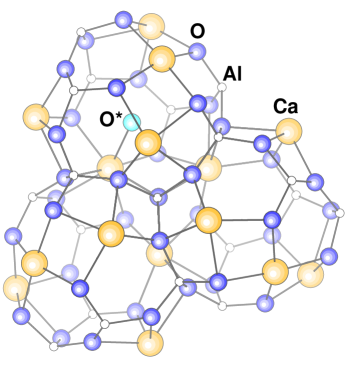
The characteristic feature of mayenite, Ca12Al14O33, is its nanoporous zeolite-like structure [6]: the unit cell with two formula units contains 12 cages of minimal diameter 5.6 Å across (cf., Fig. 1). This framework includes 64 of the oxygen atoms; the remaining two O2- ions (abbreviated as O∗ hereafter) provide charge neutrality [7] and are located inside the cages, Fig. 1. The large cage ‘entrances’ (about 3.7 Å in diameter) make it possible to incorporate H- ions into the cages according to the chemical reaction: O2-(cage) + H2(atm.) OH-(cage) + H-(another cage). The H-doped system remains an insulator – until UV-irradiation is performed. First-principles calculations have shown [8] that in C12A7:H0, the charge transport associated with the electrons excited off the H- ions occurs by electron hopping through the states of the H0 and OH- (located inside the cages) and their Ca neighbors (belonging to the cage wall). The detailed knowledge of the transport mechanism obtained for C12A7:H0 allowed prediction of ways to enhance the conductivity by increasing the concentration of hopping centers (such as encaged H0 or OH-) which would provide additional hopping paths for the carrier migration [8]. In striking contrast, whereas in C12A7:2e- the encaged O∗ ions are removed [2], i.e., all cages are empty, the conductivity is increased by 2 orders of magnitude as compared to C12A7:H0.
To understand the mechanism of the conductivity in C12A7:2e- and to determine the differences in the transport properties of these two mayenite-based compounds, we performed first-principles electronic band structure calculations of mayenite with oxygen vacancies inside the cages (i.e., with all O∗ removed) and with 2e- added as a uniform background charge to provide charge neutrality. Self-consistent solutions of the effective one-electron Kohn-Sham equations were obtained by means of the linear muffin-tin orbital method in the atomic sphere approximation [9] for the cell of C12A7:2e- with one formula unit (a total of 58 atoms per unit cell which constitute six cages) and with periodic boundary conditions. In addition, 86 empty sheres were included to fill out the open spaces of the system [10].

The calculated electronic densities of states (DOS) for Ca12Al7:H0 and Ca12A7:2e- are found to be similar, cf., Fig. 2(a) and 2(b): in both cases, oxygen 2p states form the top of the valence band, Ca 3d states form the bottom of the conduction band and a hybrid band in the band gap crosses the Fermi level making both systems conducting. Using the optical selection rules, we calculated the joint DOS that determines the positions of the characteristic absorption bands, Fig. 2(c) and 2(d). As one can see, the overall structure of the absorption spectra is similar for the two systems, and is in good agreement with experiment [1, 2]. We find: (i) in C12A7:H0, the 0.4 eV absorption peak is narrow, well-defined and separated from the 2.8 eV peak which corresponds to transitions from the occupied states of the hybrid band to the conduction band; (ii) by contrast, in C12A7:2e- the pronounced DOS at EF gives the non-zero absorption in the large wavelength limit; in addition, due to the increased width of the hybrid band, the absorption band centered at 0.4 eV substantially overlaps with the one at 2.8 eV, resulting in the observed black coloration of the samples [2].
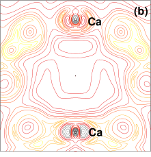
Despite the apparent similarity of the characteristic optical absorption peaks, we found that the conductivity mechanism in these two mayenite-based compounds is qualitatively different. This is clearly seen from a comparison of the charge density distributions calculated in a 25 meV energy window below EF, cf., Fig. 3. In the case of C12A7:H0, the connected charge density maxima along the hopping path demonstrates the hopping nature of the conductivity [8]. In contrast to this trapping of the electrons on particular atoms, in C12A7:2e- the conduction electrons are found to be highly delocalized. Their extended wave function suggests a bulk mechanism for the conductivity. Indeed, in C12A7:2e-, all Ca and the encaged empty spheres give comparable contributions to the DOS in the vicinity of EF (on average, 3.1 and 2.6 %, respectively), while in C12A7:H0, only four of the 12 Ca atoms, i.e., the neighbors of the encaged H0 and OH-, contribute significantly to the DOS near EF [8].

The above description of the transport properties in C12A7:H0 and C12A7:2e- differs from the original interpretation that was based on the formation of F+ centers (i.e., electron trapping on the oxygen vacancy) inside positively charged cages [1, 2, 4]. In the framework of the F+ model, the released electron could hop between empty cages (there are eight of them per unit cell) which strongly contradicts experimental observations for C12A7:H0 that the area not exposed to UV irradiation remains insulating [1, 11]. In sharp contrast to the F+ model, our calculations [8] demonstrate clearly that the conducting channels do not involve empty cages and are formed only in the UV-irradiated area because the untreated H- ions prevent the creation of such hopping paths in the light protected region – in agreement with experiment [1, 11].
Consistent with this view, we found that in C12A7:2e- the conduction electrons are not localized inside the cages, cf. Fig. 3(b). This indicates that C12A7:2e- cannot be considered to be an electride [2, 3, 4] which is essentially classifies those compounds in which the electron density is confined within structural cavities and tends to avoid the regions occupied by cations [5, 12]. Our result is in contrast with the first theoretical study of C12A7:2e- that was based on the embedded defect cluster approach [4] which excluded possibilities other than electron localization inside the cages, i.e., formation of the F+ center; strikingly, the resulting schematic picture of the energy levels (cf., Fig. 3 of the Ref. [4]) disagreed with the observed optical absorption energies [1].
Thus, our first-principles band structure calculations provide a clear physical explanation of the 100-fold enhancement of the conductivity in C12A7:2e- as compared to C12A7:H0. In the H-doped case, the released electrons migrate along a well-defined channel – the hopping path [8]. Moving one-by-one, they interact (repel) strongly with each other resulting in the formation of the parabolic Coulomb gap in the DOS at EF (cf., Fig. 2(a) inset). The value of the gap can be estimated as , where is the elementary charge, is the dielectric constant, and the characteristic distance between two electrons in the unit cell, , is equal to the cube root of the unit cell volume divided by 2. Using the lattice parameter of cubic mayenite, 11.98 Å, and =2.56 (Ref. [13]), yields 0.3 eV for the value of the Coulomb gap which agrees well with the calculated [8] splitting of the hybrid band, 0.38 eV, and with the observed [1] absorption peak at 0.4 eV.
This successful interpretation of the transport properties in C12A7:H0 suggests a way to improve the conductivity: an increased number of transport channels should alleviate the electron repulsion. Consistent with this view, a 100-fold increase of the conductivity is observed for C12A7:2e-, where, loosely speaking, the number of conducting channels can be considered very large so that the injected electrons have more freedom and the “Coulomb blockade” does not occur. Following this interpretation, we predict that even higher conductivity can be obtained in similarly treated Si-substituted mayenite, [Ca12Al10Si4O32]6+(6e-), where two additional oxygen vacancies inside the cages would result in a three-fold increase of the carrier concentration (up to 71021 cm-3) in this material [14].
Finally, we stress that the enhanced conductivity in C12A7:2e- comes at the cost of greatly increased optical absorption. The latter occurs due to the increase of (i) the density of states of the hybrid band in the band gap and (ii) the width of this hybrid band – resulting in intense transitions from the occupied states of the hybrid band to the conduction band in the visible range which excludes the possibility of using this oxide as a transparent conducting material. Fortunately, the details of the electronic band structure and the conductivity mechanism found here will help in the search for new candidates with improved optical and transport properties.
We thank M. I. Bertoni and T. O. Mason for close collaboration in carrying out suggested conductivity measurements for the UV-light protected C12A7:H0 samples. Work supported by the DOE (grant N DE-FG02-88ER45372) and the NSF through its MRSEC program at the Northwestern University Materials Research Center. Computational resources have been provided by the DOE supported NERSC.
REFERENCES
- [1] K. Hayashi, S. Matsuishi, T. Kamiya, M. Hirano, and H. Hosono, Nature 419, 462-465 (2002).
- [2] S. Matsuishi, Y. Toda, M. Miyakawa, K. Hayashi, T. Kamiya, M. Hirano, I. Tanaka, and H. Hosono, Science 301, 626 (2003).
- [3] J. L. Dye, Science 301, 607 (2003).
- [4] P. V. Sushko, A. L. Shluger, K. Hayashi, M. Hirano, and H. Hosono, Phys. Rev. Lett. 91, 126401 (2003); P. V. Sushko, A. L. Shluger, K. Hayashi, M. Hirano, and H. Hosono, Thin Solid Films 445, 161 (2003).
- [5] J. L. Dye, Inorg. Chem. 36, 3816 (1997).
- [6] H. Bartl, and T. Scheller, Neues Jb. Miner. Mh. 35, 547-552 (1970); A. N. Christensen, Acta Chem. Scand., Ser. A 41, 110 (1987).
- [7] J. A. Imlach, L. S. D. Glasser, and F. P. Glasser, Cement Conc. Res. 1, 57-61 (1971).
- [8] J. E. Medvedeva, A. J. Freeman, M. I. Bertoni, and T. O. Mason, arXiv:cond-mat/0402218, submitted to Phys. Rev. Lett.
- [9] O. K. Andersen, O. Jepsen, and M. Sob, Electronic band structure and its applications, (ed. Yussouff, M. Springer-Verlag, Berlin, 1986).
- [10] J. Keller, J. Phys. C 4, L85 (1971).
- [11] M. I. Bertoni, and T. O. Mason, unpublished.
- [12] Z. Li, J. Yang, J.G. Hou, and Q. Zhu, J. Am. Chem. Soc. 125, 6050 (2003).
- [13] G. I. Zhmoidin, and G. S. Smirnov, Inorg. Mater. 18 1595-1601 (1982).
- [14] J. E. Medvedeva, A. J. Freeman, M. I. Bertoni, and T. O. Mason, to be published.