Atom Chips: Fabrication and Thermal Properties
Abstract
Neutral atoms can be trapped and manipulated with surface mounted microscopic current carrying and charged structures. We present a lithographic fabrication process for such atom chips based on evaporated metal films. The size limit of this process is below 1m. At room temperature, thin wires can carry more than 107A/cm2 current density and voltages of more than 500V. Extensive test measurements for different substrates and metal thicknesses (up to 5 m) are compared to models for the heating characteristics of the microscopic wires. Among the materials tested, we find that Si is the best suited substrate for atom chips.
pacs:
Manipulation of neutral atoms using micro-structured surfaces (atom chips) has attracted much attention in recent years Folman et al. (2002). Atom chips promise to combine the merits of microfabrication and integration technologies with the power of atomic physics and quantum optics for robust manipulation of atomic quantum systems. Extreme and precise confinement in traps with large level spacing is possible. Neutral atoms have been trapped by currents flowing in microscopic wires fabricated on the atom chip surface Reichel et al. (1999); Folman et al. (2000), manipulated by electric fields Krüger et al. (2003), and even cooled to Bose-Einstein condensates Ott et al. (2001); Hänsel et al. (2001); Schneider et al. (2003).
The demands on atom chips are high current densities to create steep traps, and small structure sizes to create complex potentials at a scale where tunneling and coupling between traps can become important. Exceptional high-quality fabrication is essential, since the smallest inhomogeneities in the bulk of the wire or the fabricated edges can lead to uncontrolled deviations of the current flow and therefore to disorder potentials in the magnetic guides and traps Fortagh et al. (2002a); Jones et al. (2003); Leanhardt et al. (2003); Wang et al. (2004); Esteve et al. (2004).
The fabrication process preferred by groups working in the field is to grow thick wires from a thin patterned layer using electroplating Drndić et al. (1998); Fortagh et al. (2002b); Lev (2003), which allow large currents for trapping and manipulating the atoms.
In contrast, we have chosen to directly pattern up to 5m tall evaporated high-quality layers of gold using a photolithographic lift-off technique (Fig. 1). Wires are defined by thin gaps in the evaporated gold surface. These m sized gaps only produce an insignificant amount of stray light when the gold surface is used as a (nearly perfect) mirror for laser cooling and atom imaging. This technique was preferred because it results in high surface quality and very smooth structure edges.
In our process, the substrate (Si or GaAs covered with a SiO2 insulation layer or sapphire) is prepared with an adhesion primer. To allow the evaporation of thick metal layers, we spin up to 5m thick films of image reversal photoresist (AZ 5214E) onto the sample at low speed. The resist is then exposed to UV-light through an e-beam patterned mask. After developing the resist structure (Fig. 1A), a Ti adhesion layer (35nm) and a thick Au layer (1–5m) are evaporated at a short distance from the source at a rate of 5–40Å/s. To achieve good surface quality, care has to be taken in controlling the evaporation speed and substrate temperature. The gold covered resist structure is then removed in a lift-off procedure using acetone (if necessary in a warm ultrasonic bath) and isopropanol as solvents. A second gold layer can be added by repeating the above process. Some chips were covered with a thin protective insulation layer of Si3N4. Finally, the chips are cut or cleaved to the desired dimensions of mm2.
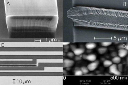
The resulting gold surfaces (Fig. 1D) are smooth (grain sizes nm), and the wire edges are clearly defined. The surface quality depends on adhesion properties and the substrate smoothness. Semiconductor substrates (Si and GaAs) gave better results than sapphire samples.
An important characteristic of atom chips is how much current and voltage the microscopic wires can carry. The achievable confinement of the atoms depends on the maximal potential gradient, which scales with the achievable current density .
To evaluate the fabrication process and to collect comprehensive data for the operation of the atom chips and their limits, a series of test chips was built incorporating 2mm long wires with widths of 2, 5, 10, 50, and 100m and heights ranging from 1-5m on different substrates (Si with 20nm or 500nm thick isolation layer, GaAs, and sapphire). The test chips were mounted on a simple sample holder, and the current and voltage characteristics were measured under moderate vacuum conditions (mbar).
Regarding charges, both semiconducting (Si) and insulating (sapphire) substrates tolerated voltages of V (V for sapphire) across a gap of 10m. This provides ample flexibility for manipulation of atoms in comparably deep potentials even at relatively large distances from the surface by means of electrostatic fields Krüger et al. (2003).
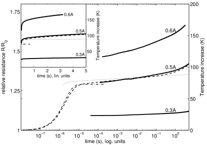
The current characteristics were measured by pushing a constant current through the wire and recording the voltage drop, which yields the resistance of the wire. The experiments were carried out in a pulsed manner similar to the real atom chip experiments, allowing a cool down time (typically s) between the pulses. Usually, we arranged the length of the current pulses such that the resistance rose by less than 50%. This proved to be a safe procedure without damaging the wires. At stronger heating, the measurements were partly irreproducible (sometimes the wires were even destroyed).
The measurements show two timescales for the heating process (Fig. 2). Immediately after switching the current, the wires heat up on a s timescale, seen as an increased resistance in our experiments. This initial jump, which was not resolved in our measurements, is followed by a slow rise of temperature, which was observed over the full duration of the current pulses (up to 10s).
In order to gain insight into the relevant processes and parameters, we compared our data with a simple model for the heating of the substrate mounted wires. The heat created in a wire of height and width carrying a current density is given by ohmic dissipation. Essentially, the heat is removed through heat conduction to the substrate, as thermal radiation is negligible for the observed temperatures. The temperature evolution of the wire is determined by the heat flow through the interface, which exhibits a thermal contact resistance (thermal conductance ), and the heat dissipation within the substrate, governed by the heat conductivity and heat capacity (per volume) . This leads to two very different timescales for the heat removal:
The timescale of the first process (heat flow from the wire to the substrate through the isolation layer) is given by where is the heat capacity (per volume) of the wire, its (cold) resistivity with a linearly approximated temperature coefficient . For typical parameters of our chips, this timescale (s) is so short that the temperature difference between the wire and the substrate
| (1) |
saturates practically instantaneously, unless exceeds the limit of . In this case, an exponential rise of the temperature will lead to an almost instantaneous destruction of the wire.
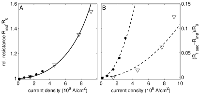
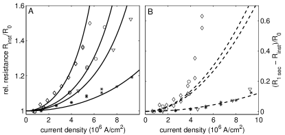
Our model for the fast heating process quantitatively agrees with the data. While the initial temperature rise is independent of the wire width (Fig. 3A), it depends on the contact resistance to the substrate (Fig. 4A). The latter effect can clearly be seen by comparing the data for two Si substrates with different insulation layers. A 500nm thick SiO2 layer leads to stronger heating than a 20nm thick layer. In order to find the optimal substrate, the values for the thermal conductance were obtained from fitting the model to our data (W/Km2 for Si with 20nm SiO2, sapphire, Si with 500nm SiO2, and GaAs, respectively). The fitting is necessary, because includes the conductance through the insulation layer and the contact resistances at the individual material interfaces. The best conductance was found for the Si substrate with the thin SiO2 layer. The differences between the remaining data are mainly due to different wire heights. In our experiments Si substrates with thin isolation layers consistently exhibited the lowest fast heating of typically K corresponding to % resistance increase at A/cm2.
In a two dimensional model for the heat transport within the substrate, we assume a line-like heat source on the surface of a half space substrate. The temperature increase at this point is then given by the incomplete function
| (2) |
Here, the (small) temperature dependence of the resistivity is neglected.
For this slow heating process, the total heat dissipation becomes important. Hence, wider wires heat up faster than narrow ones for equal current density (Eq. 2 and Fig. 3 B). In addition, the heat transport in Si is faster than in the other tested materials due to its larger heat conductivity (). Fig. 4 shows that the thin wires (m) mounted on Si heat up significantly less than the taller wires (m) fabricated on sapphire or GaAs. In the latter case, the simple model underestimates the temperature rise for large power dissipation as predicted by the numerical heat equation integration. The analytical model is only valid as long as the substrate can be treated as a heat sink. For a thin substrate (typically 700m) the heat transport out of the substrate has to be taken into account for longer times (typically after a few 100ms). Then a two-dimensional numerical calculation accurately reproduces the data (Fig. 2).
To conclude, we have presented a method for fabricating atom chips with a lithographic lift-off process. With this process we produced wires that can tolerate high current densities of A/cm2. We have shown that the temperature evolution of surface mounted microwires agrees with a simple dissipation model. The optimal substrate has a large heat conductivity and capacity and is in good thermal contact with the wire. Si substrates with thin oxide layers showed the best thermal properties of the examined samples as well as good surface qualities. The described fabrication process leads to very accurate edge and bulk features. As a result, the disorder potentials have been observed to be sufficiently small not to fragment a cold thermal atomic cloud (K) at a distance of m from the wire Kru et al. (2004).
We thank T. Maier and K. Unterrainer of the Mikrostrukturlabor der TU-Wien for valuable discussions and their insight in developing the initial fabrication process this work is based on, O. Raslin for her help in the fabrication process and C. Becker and A. Mair for their help with the test measurements. This work was supported by the European Union, contract numbers IST-2001-38863 (ACQP) and HPRI-CT-1999-00114 (LSF) and the Deutsche Forschungsgemeinschaft, Schwerpunktprogramm ‘Quanteninformationsverarbeitung’.
References
- (1)
- Folman et al. (2002) R. Folman et al., Adv. At. Mol. Opt. Phys. 48, 263 (2002).
- Reichel et al. (1999) J. Reichel et al., Phys. Rev. Lett. 83, 3398 (1999).
- Folman et al. (2000) R. Folman et al., Phys. Rev. Lett. 84, 4749 (2000).
- Krüger et al. (2003) P. Krüger et al., Phys. Rev. Lett. 91, 233201 (2003).
- Ott et al. (2001) H. Ott et al., Phys. Rev. Lett. 87, 230401 (2001).
- Hänsel et al. (2001) W. Hänsel et al., Nature 413, 498 (2001).
- Schneider et al. (2003) S. Schneider et al., Phys. Rev. A 67, 023612 (2003).
- Fortagh et al. (2002a) J. Fortagh et al., Phys. Rev. A 66, 041604(R) (2002a).
- Jones et al. (2003) M. P. A. Jones et al., Phys. Rev. Lett. 91, 080401 (2003).
- Leanhardt et al. (2003) A. E. Leanhardt et al., Phys. Rev. Lett. 90, 100404 (2003).
- Wang et al. (2004) D.-W. Wang et al., Phys. Rev. Lett. 92, 076802 (2004).
- Esteve et al. (2004) J. Estève et al., physics/0403020.
- Drndić et al. (1998) M. Drndić et al., Appl. Phys. Lett. 72, 2906 (1998).
- Fortagh et al. (2002b) J. Fortagh et al., Appl. Phys. Lett. 81, 1146 (2002b).
- Lev (2003) B. Lev, Quant. Inf. Comp. 3, 450 (2003).
- Kru et al. (2004) P. Krüger et al., to be published (2004).