The electronic structure around As antisite near (110) surface of GaAs
Abstract
The electronic structure around a single As antisite in GaAs is investigated in bulk and near the surface both in the stable and the metastable atomic configurations. The most characteristic electronic structures of As antisite is the existence of the localized p-orbitals extending from the As antisite. The major component of the highest occupied state on As antisite in the stable configuration is s-orbital connecting with neighboring As atoms with nodes whereas that in the metastable configuration is p-orbital connecting without nodes. Localized p-orbitals on the surrounding As atoms around the As antisite exist in every configuration of As antisite. Such features are retained except the case of the As antisite located just in the surface layer in which the midgap level is smeared into the conduction band and no localized states exist near the top of the valence band. Scanning tunneling microscopic images of defects observed in low-temperature grown GaAs, possibly assigned as As antisite, the origin of the metastability, and the peculiarity of the defects in the surface layer are discussed.
pacs:
73.20.Hb, 61.72.Ji, 68.37.Ef, 71.55.-iI Introduction
Bulk GaAs crystals grown under As-rich conditions are known to contain As-related defects called EL2 centers Kamińska and Weber (1993) that form a deep double donor level at the middle of the band gap. The EL2 centers compensate residual shallow acceptors thus giving the crystals a semi-insulating property useful for device applications. The EL2 centers induce a characteristic optical absorption extending to the sub-band gap region with a spectral hump peaking around 1.2 eV. The most peculiar feature of the EL2 centers is the photoquenching effect in which the EL2-originated optical absorption becomes diminished when the crystal is optically illuminated with an intra-center excitation at low temperatures. Martin (1981) The centers once quenched are, however, recovered if the crystal is heated or illuminated with a different infrared light. Fischer (1987) This reversibility and the lost of the effect at high temperatures indicate that the EL2 centers, when they are electrically neutral, are transformable between the stable () and the metastable () state.
For the atomic structure of EL2 centers, the most commonly accepted model is isolated arsenic antisite defects (). First principle calculations Chadi and Chang (1988); Dabrowski and Scheffler (1988) based on the model showed that the metastable may be a close pair of an interstitial arsenic () and a gallium vacancy () that is formed by the displacement of the antisite As atom from the lattice point to a puckered interstitial position in a [111] direction leaving a behind. The point symmetry lowering from to by the displacement was supported by optical absorption experiment. Trautman and Baranowski (1992) However, the atomic structure of and have been controversial since some defects, though exhibiting features of EL2 centers, were found to show no photoquenching effect. Omling et al. (1986); Manasreh et al. (1990) The presence of such variations in EL2-like centers arose an argument that the EL2 centers form a ‘family’ including various structures rather than have a unique atomic configuration. Taniguchi and Ikoma (1983)
Low-temperature grown (LT-) GaAs crystals homoepitaxially grown under an excess As pressure contain a high density of As-related defects. Feenstra and his coworkers Feenstra et al. (1993) applied scanning tunneling microscopy (STM) to atomic level observations of individual point defects abundantly found in LT-GaAs epifilms. Four different defect contrasts observed in different sizes were attributed to atoms located in different depths from the sample surface. Recently, some of the present authors Hida et al. (2001) provided direct evidence for the defect being EL2: They found that the STM contrasts of the defects in LT-GaAs samples kept at a low temperature (90K) are drastically changed by light illumination with an excitation spectrum nearly identical to that for the photoquenching effect of EL2 centers in bulk crystal. The local density of states (DOS) measured by scanning tunneling spectroscopy (STS) at the defect sites shows that the donor gap state present in the normal state disappears in the metastable state, conforming the characteristics of EL2.
Theoretically simulated STM images of defects show an apparently good agreement with experimental images as far as the defects in the second largest contrast Feenstra et al. (1993) are concerned. Capaz et al. (1995); Zhang (1999) However, no systematic comparison has been made for the STM image contrasts in other sizes and those in the metastable state. foo
In this paper, we will report results of first principle electronic structure calculations of an in GaAs bulk crystal and those near the surface, both in the stable and the metastable state. The main aim of the present study is to answer a naïve question if defects near the surface that can be probed by STM may be substantially different or not in the structures and physical properties from the defects in the bulk crystals. In Sec. II, we describe the methods of calculations based on the atomic structure models. In Sec. III, we show the electronic structures of the highest occupied level in real space and discuss the nature of the level which differs depending on the depth of the from the surface. Section IV is devoted to a comparison between the simulated STM images and experimental ones and discussions about the effects of surface on the properties of centers in light of the calculated electronic structures. In Sec. V, we conclude this paper.
II Computational Details
Since a considerable lattice expansion is present around defects due to the antibonding nature of the double donor level in the band gap, Bonapasta and Giannozzi (2000) it is needed to calculate the electronic structure allowing lattice relaxation with sufficient accuracy. For this purpose, we used the density-functional (DFT) theory with the local-density approximation (LDA) employing two different methods for electronic structure calculations. One is the method using the norm-conserving pseudopotential of the Troullier-Martin type with the plane wave basis set Troullier and Martins (1991) and the other is the tight-binding Linear Muffin-Tin Orbital (LMTO) method. Andersen and Jepsen (1984)
In the case of the norm-conserving pseudopotential of the Troullier-Martin type, we adopt a supercell and the cut-off energy for the plane wave basis was set to be 10 Rydberg. The -point sampling in the Brillouin zone was done only at the point. We relaxed atomic positions, and calculated the electron density with the plane wave basis.
The LMTO basis is localized around each atom and hence we can analyze the contribution of the atomic orbital to a specific energy state in concern. The LMTO basis set is minimal and each basis function can be described by a small number of parameters so that we can perform calculations with relatively small memory and computing time.
The procedure for calculating the electronic structures
in the model system that is bounded with a surface and contains
an defect is as follows:
(1) Relaxing a relatively small lattice system with an and a surface by the pseudopotential method.
(2) Embedding the relaxed small system in a larger perfect lattice
with the atomic configuration around the unchanged.
(3) Calculating the electron density with point
in a supercell by the pseudopotential method, and other properties
such as the relation,
the total density of states (DOS) and local density of states
(DOS) of each atom by the tight-binding LMTO method.
For defects in bulk crystals, we introduced an defect by replacing a Ga atom with an As atom in a cubic unit cells containing 64 atoms. These atoms were then subject to relaxation by means of the molecular dynamics with plane wave bases. The lattice constant was fixed to the experimental value 5.654 Å during the relaxation. We found that the distances between the and the neighboring atoms after relaxation are similar to the previous results. Kaxiras and Pandey (1989); Bonapasta and Giannozzi (2000)
For calculations of the defect structure in the metastable state, we first displaced the atom tentatively by 1.2 Å from the lattice point to a puckered interstitial position along a bond breaking [111] direction, and then relaxed the lattice by means of the molecular dynamics with plane wave bases. The resultant distance after the relaxation between and a neighboring As atom on the axis of the symmetry was 1.37 Å, a little larger than the previous values. Chadi and Chang (1988); Dabrowski and Scheffler (1988, 1989) The electron density were calculated for the perfect lattice of this size (64 atoms) and for lattices in an extended size of (192 atoms) in which we embedded a relaxed supercell containing an or an - pair. In these calculations, we fixed the atoms beyond the third neighbors at the perfect lattice positions.
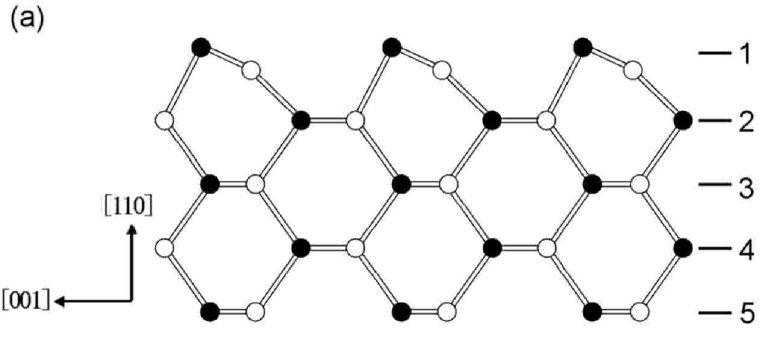
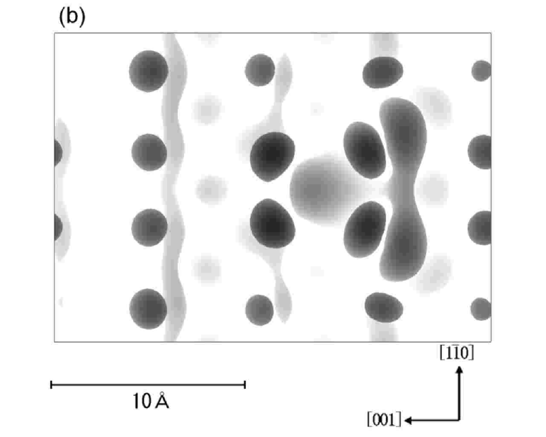
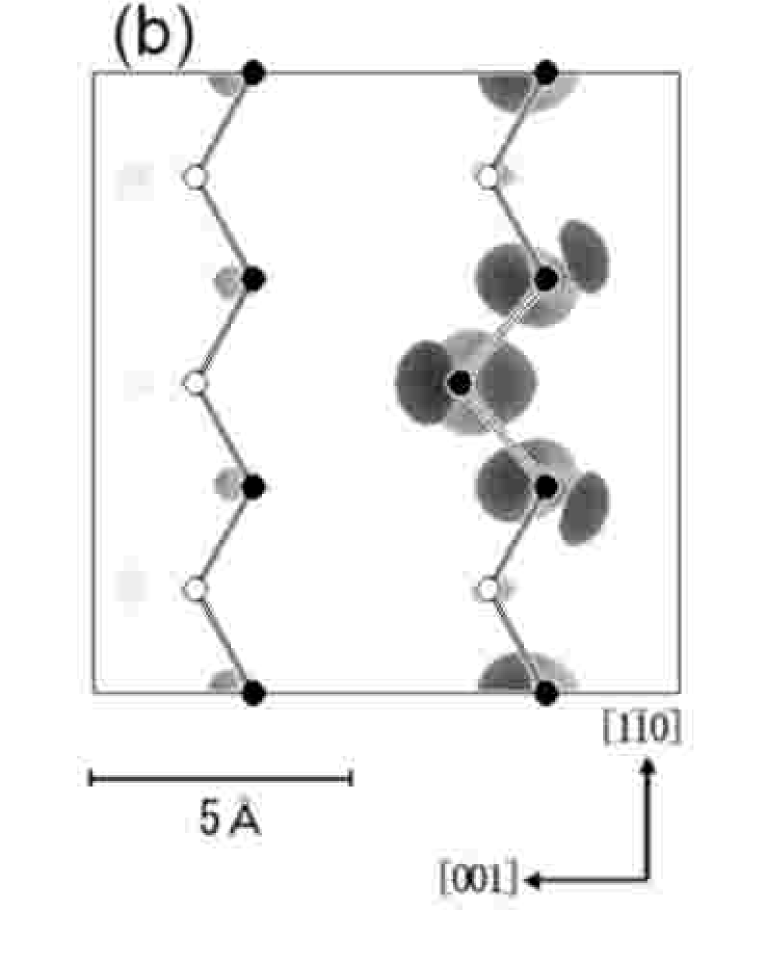
For defects near a (110) surface, we prepared a slab lattice parallel to the (110) plane in which one surface was relaxed and the other surface was terminated with hydrogen atoms. For convenience, we refer to the surface layer without hydrogen, though buckled as shown in Fig. 1(a), as ‘layer 1’, the one layer down as ‘layer 2’, one more layer down as ‘layer 3’ and so on. The electronic structures of the system bounded with surfaces were calculated for various configurations: without defects, with an defect (the stable state) located in the layer 1 to the layer 4.
The procedure of lattice relaxation and electronic structure calculations are as follows. We first relaxed the surface bounded slab of a lateral size of and a thickness of 7 layers including the layer of hydrogen atoms. The lattice constant was fixed in this case too. The positions of atoms in the relaxed configuration displaced from those of the ideal atomic positions are smaller than 0.2 Å, 0.1 Å and 0.05 Å for the first, the second and the third neighbor atoms of , respectively. Some of the neighbor atoms were displaced considerably, especially near the surface. For example, for an located on the layer 2, the third neighbor atoms on the layer 1 were displaced by 0.063 Å, whereas the third neighbors on the layer 3 only by 0.019 Å. Therefore, the atoms at shallow depths from the surface were not fixed tightly while the atoms further than third neighbors were fixed since all these atoms, even if relaxation was allowed, were found to be displaced by only a magnitude smaller than 0.07 Å. After relaxing the small system, we embedded it in a larger system with a surface of a size of and 5 layers including the hydrogen layer. For an on the layer 4, we embedded the relaxed system in a still larger system of the same surface size but of 6 layers in thickness.
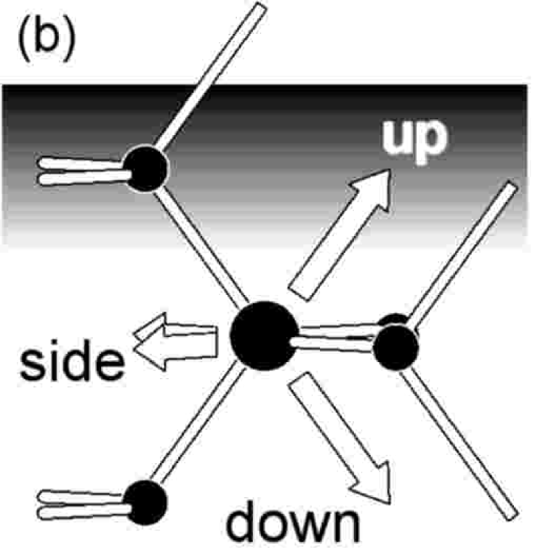
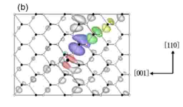
For calculations of metastable - pairs, we should note that there are three inequivalent configurations regarding the displacement direction relative to the surface as shown in Fig. 1(b). We hereafter call the “up” configuration for the displacement direction ascending to the surface, the “side” configuration for the direction parallel to the surface, and the “down” configuration for the direction descending from the surface. The lattice relaxed to a metastable configuration similar to that in the bulk crystal except for atoms on the layer 1, where the similar displacement of the surface atoms would destabilize the surface buckling and therefore is energetically unfavorable.
According to Tersoff-Hamann theory, Tersoff and Hamann (1985) filled-state STM images under a negative sample bias of V, the bias condition experimentally employed in the previous study, Hida et al. (2001) were simulated by taking into account only the highest occupied state that should give the main contribution to the contrast. The image was calculated as a two-dimensional contour map of the iso-surface of electron density of the highest occupied state in vacuum out of the surface.
III Electronic Structure
III.1 As antisite in bulk crystal
III.1.1 Stable configuration
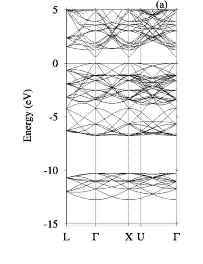
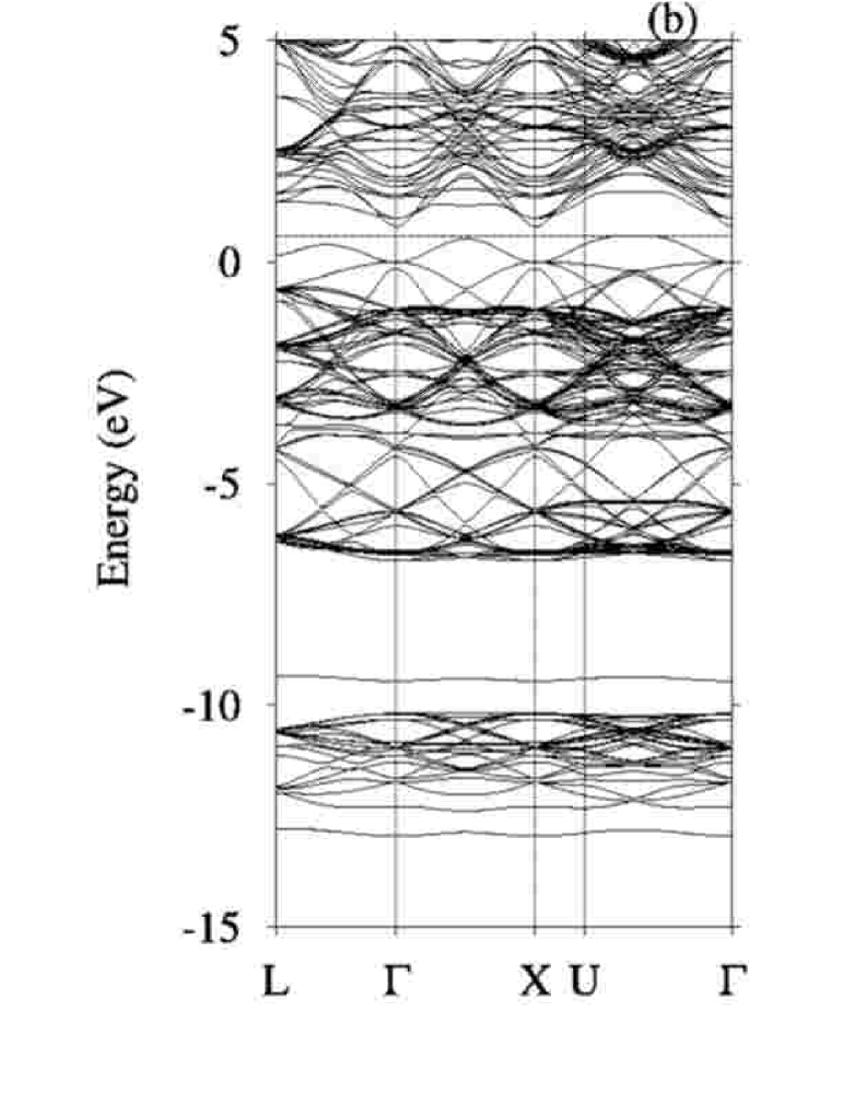
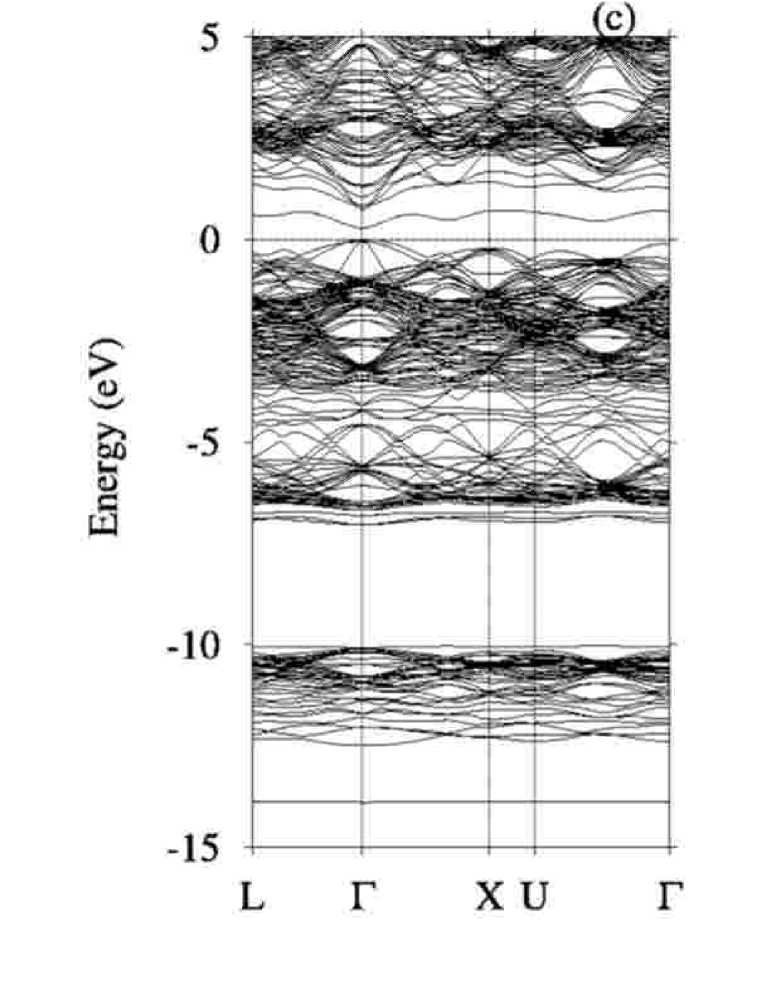
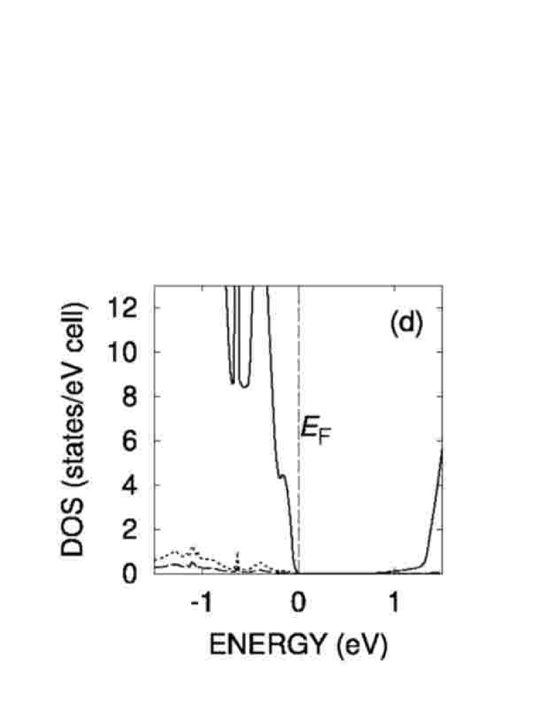
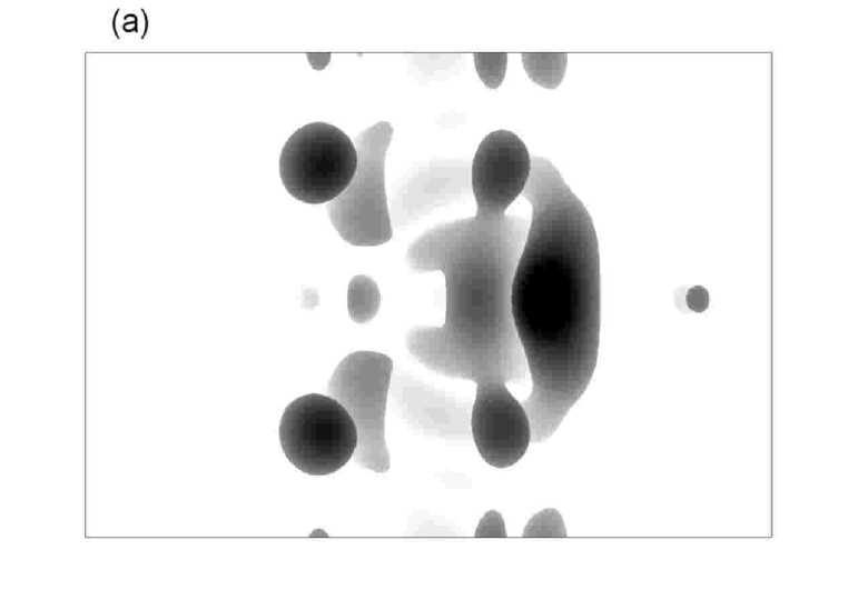
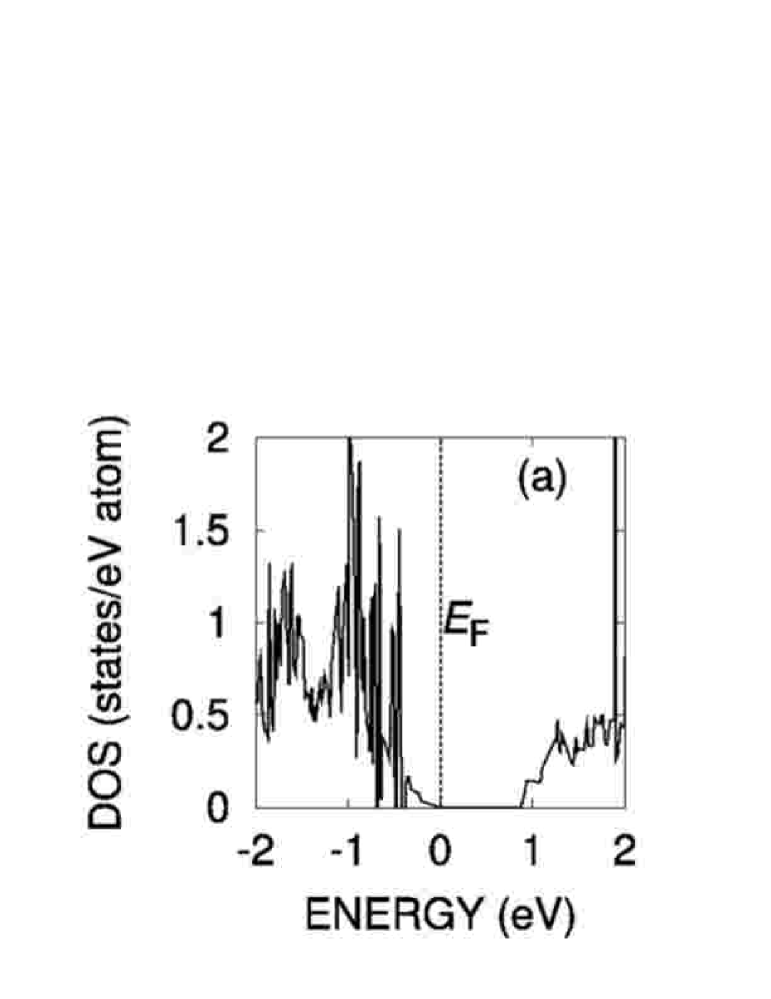
Figures 2(a) and 2(b) show the relations calculated by the LMTO method in a bulk system with a unit cell of 64 atoms. Figure 2(a) is that of the perfect lattice and 2(b) that of the lattice containing an atom in the stable configuration. The band structure of the perfect lattice is characterized by three bands with energy gaps, the As s band below eV, the valence band between eV and eV, and the conduction band above the energy gap. An atom in the stable configuration introduces an occupied band with relatively small dispersion in the band gap as shown in Fig. 2(b). The DOS of perfect lattice and that of the lattice containing an in the stable configuration are shown in Figs. 2(d) and 2(e) respectively. Comparison between the two figures indicates that atom introduces the gap state mainly localized at the atom and neighboring four As atoms.
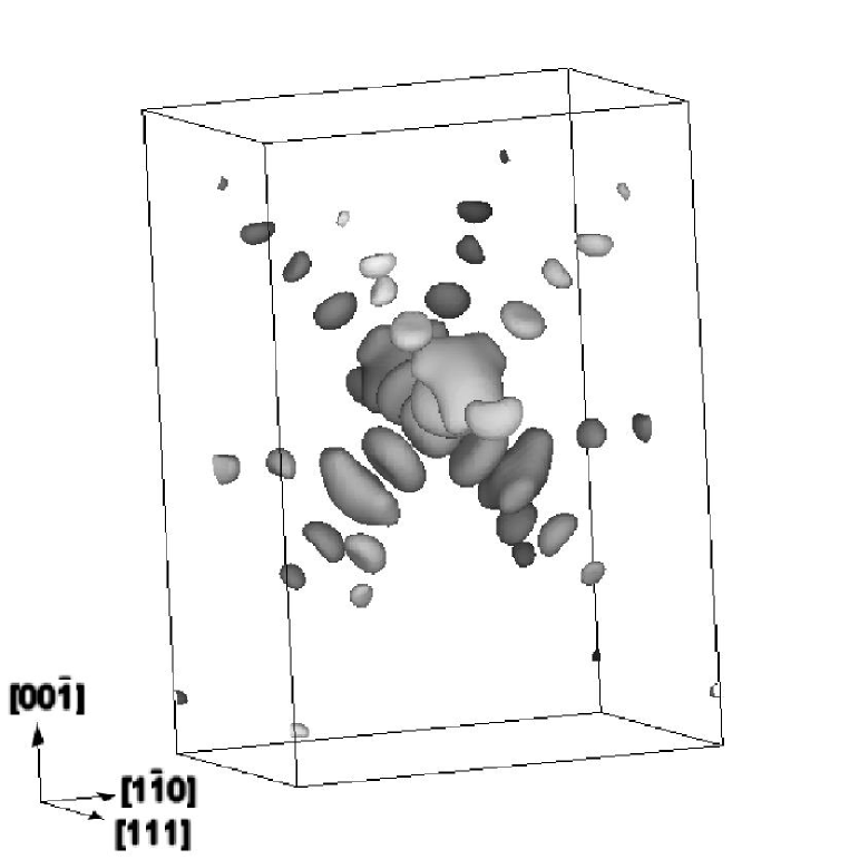
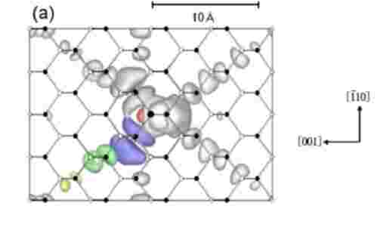
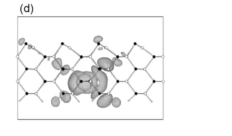
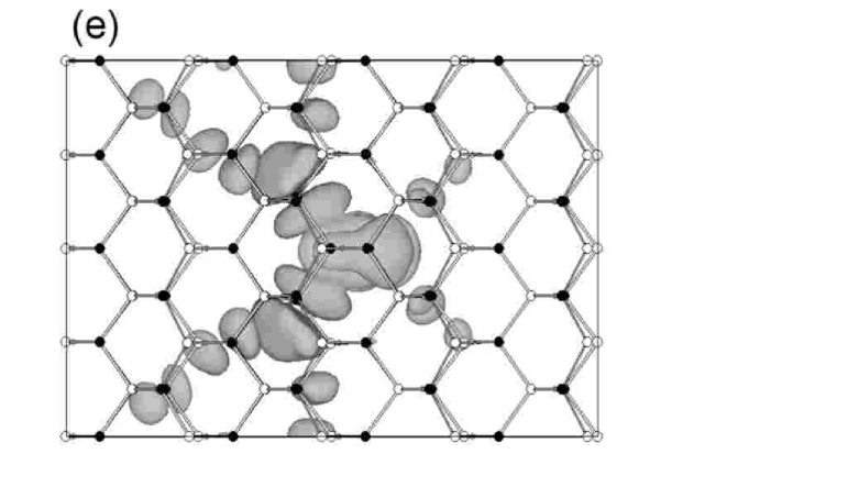
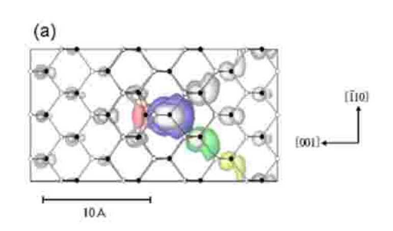
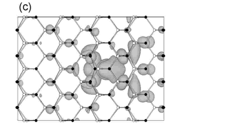
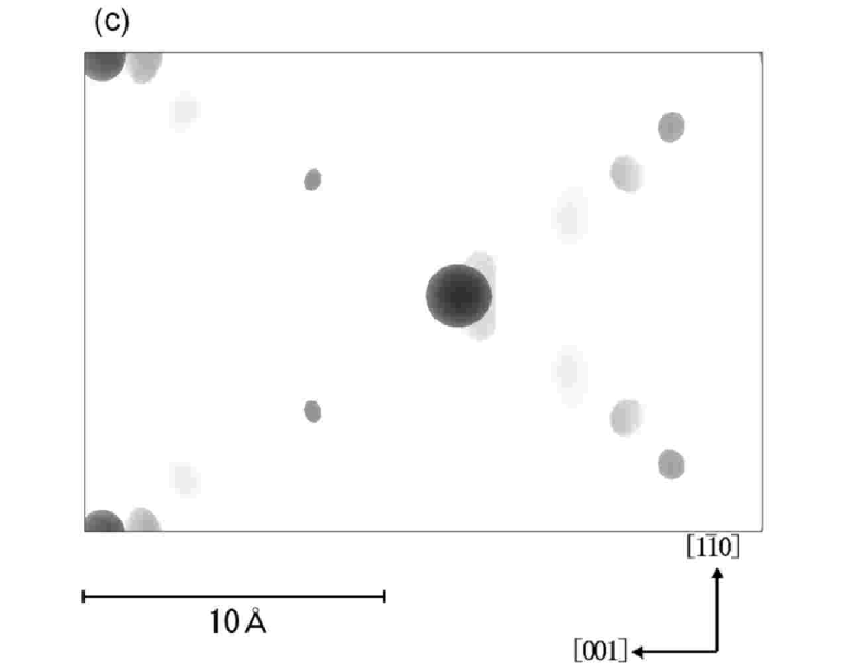
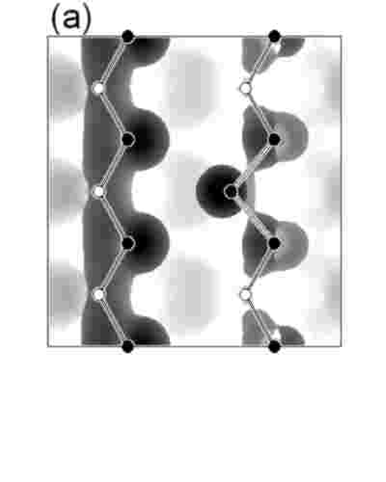
Figure 3 shows the iso-surface of electron density of the highest occupied state in the gap calculated by the plane wave basis for a system of 192 atoms containing an in the stable configuration. One may see the symmetric structure extending first along four [111] directions and then each further branching out along three [110] directions. The decreasing electron density with distance from the shows the localized nature of the corresponding DOS at the atom (Fig. 2(e)). The iso-surface of electron density is shown also in Figs. 4(a) and 4(b). We note that the electron density at the site is s-like (colored in red) and those on the nearest neighbor As sites are p-like (colored in blue) with the lobes heading toward the atom. These p-like iso-surface are respectively linked to the central s-like iso-surface with a distinct node. The electron density on the third nearest neighbor As atoms are also p-like (colored in green) with the lobes aligning in the same directions as those of the first neighbor As atoms and the fifth neighbors (colored in yellow) again forming nodes between them. Thus, the electronic structure of the highest occupied level in the stable configuration has a radial pattern that are characterized by the mutually anti-bonding As p-orbitals.
The defect formation energy of in the unit cell of 64 atoms, is written in As-rich limit as Zhang and Northrup (1991)
| (1) |
where is the total energy of the system with , is the chemical potential of electron, is the energy per atomic pair of bulk GaAs, and is the energy per atom of pure bulk As. is the charge of the defect, and and are the numbers of atoms of each species in the system. The defect formation energy is estimated to be 0.6 eV by using the point sampling for the total energy calculation. However, this total energy is underestimated since, as seen in the Fig. 2(b), point is the bottom of the dispersion of the midgap impurity level. Since the peak of the midgap impurity level locates at 0.31 eV above its bottom, the amount of underestimated energy would be 0.6 eV. By adding it to the total energy, we estimate the defect formation energy to be 1.2 eV. This value is consistent with those of the previous calculations 1.4-1.8 eV. Zhang and Northrup (1991); Schick et al. (2002)
III.1.2 Metastable configuration
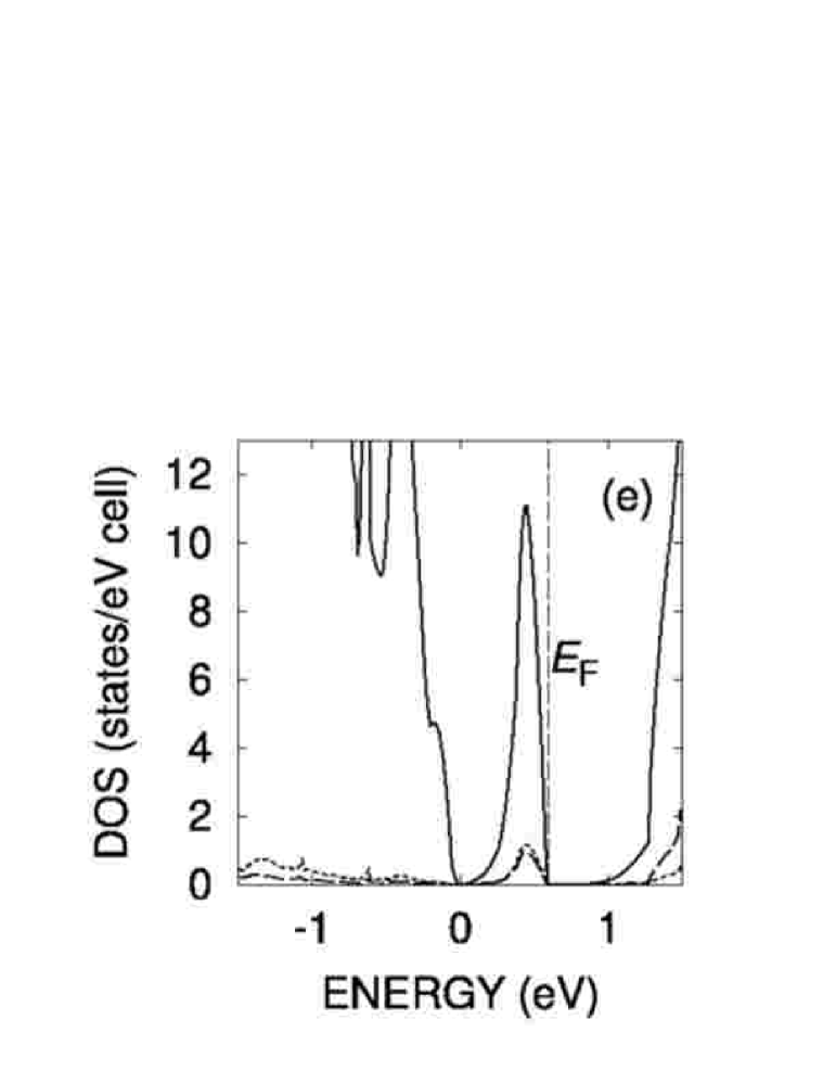
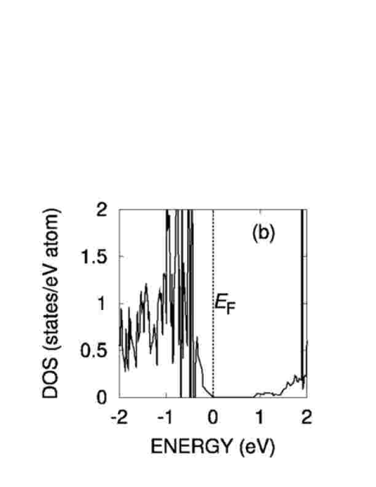
Figures 2(c) and 2(f) show the relation, the total DOS and the DOS calculated by the LMTO method for a system with a unit cell of 64 atoms containing an atom in the metastable configuration (-) that was fully relaxed by the pseudopotential method. The analysis of the DOS shows that the basis function localized at the atom constitutes the main contribution to the lowest unoccupied states introduced in the band gap between the valence band and the conduction band. Instead, there are no occupied states associated with localized orbitals at the atom near the Fermi level. This implies that the lowest unoccupied states and the highest occupied states in the stable configuration exchange their energetic order in the metastable configuration. However, the position of the unoccupied level in the gap was found to be sensitive to the computational detail. For instance, a pseudopotential calculation with a larger supercell shifts this unoccupied level to a slightly higher energy position in the conduction band region.
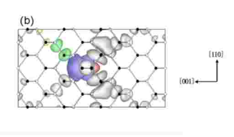
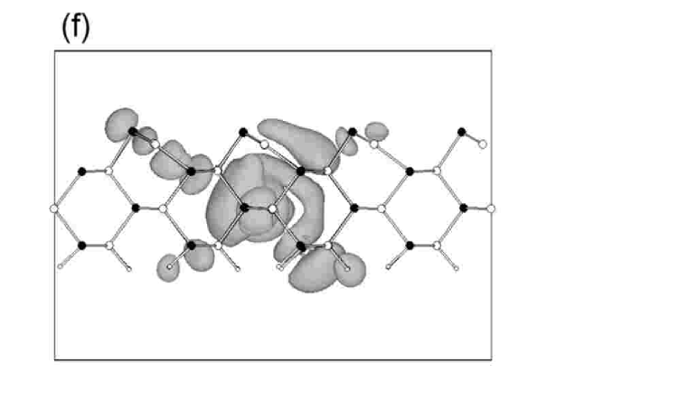
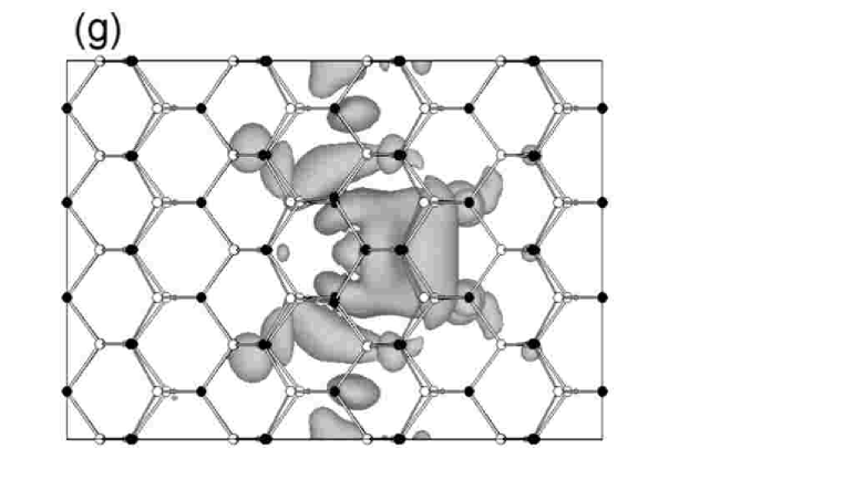
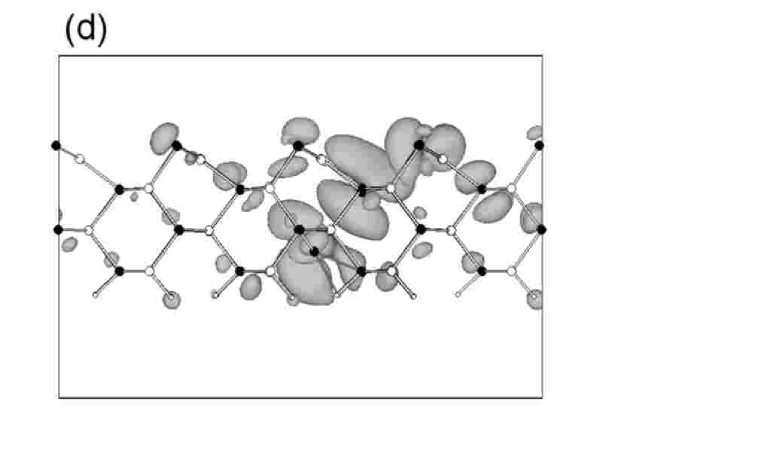
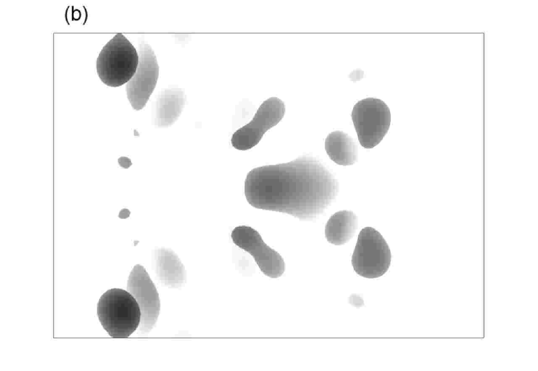
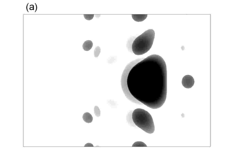
Figures 5(a) and 5(b) show the electron density of the corresponding highest occupied state of the system of 192 atoms containing a relaxed - pair. The electron density of this state extends over a wider range and differs substantially from the symmetric radial pattern in the stable configuration shown in Figs. 4(a) and 4(b). The less localized feature is consistent with the large dispersion of the highest occupied band that merges into the bulk valence bands as seen in Fig. 2(c). We should note that the iso-surface of the electron density at the atom becomes p-like in the metastable configuration in contrast to the s-like feature in the stable configuration. The p-like iso-surface at the is in parallel to those of the three neighboring As atoms with no nodes between them. The radial pattern characteristics of the stable configuration is broken to . Among the iso-surface branches extending in four [111] directions, the branch remained is only the one in the direction opposite to the displacement direction of the atom. The lobe of the branch, however, preserves the p-like anti-bonding character as in the stable configuration.
III.2 As antisite located near (110) surface
III.2.1 Stable configuration
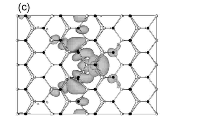
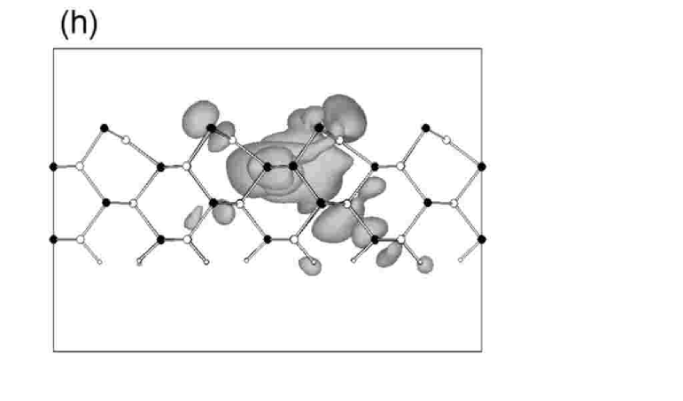
For slab systems with a surface, the electronic energy levels were calculated only by the pseudopotential method with plane wave basis. Except for the located in the surface layer (the layer 1), the highest occupied state remains amid in the band gap as in the bulk crystal. The absence of the gap state associated with located in the layer 1 is shown also by the DOS calculated by the LMTO for a system of 60 atoms with the surface size of and the thickness of 5 layers terminated with hydrogens on one side. Figures 4(c)-(j) show the iso-surfaces of electron density of the highest occupied states in the gap for an located in the stable configuration in the layer 1-4. In all the cases, the features of the iso-surface is essentially the same as those in the bulk crystal (Figs. 4(a) and 4(b)): the s-like feature at the site and the p-like ones at the neighboring As atoms. The radial pattern characteristics of the highest occupied state in the bulk crystal look as if it were just terminated with the surface. Even in the located in the layer 2 (Figs. 4(g) and 4(h)), though the electron density is concentrated mainly on the first and the third neighbor As atoms near the surface with more distinct p-like features than in the bulk lattice, the atomic configuration around the almost remains the same as in the bulk lattice. The located in the layer 3 (Figs. 4(e) and 4(f)), however, shows a subtle difference in the iso-surface from that in the bulk crystal. The p-like iso-surface at the first nearest As atom extends considerably to Ga atoms in the layer 1 forming -like bonds without a node. This may be an effect of the surface buckling: For the surface Ga, As in the layer 2, and , the angle of Ga-As-is at 87∘, which is approximately right angle, so that the p-orbitals on the As atoms can easily form bonds. The situation is quite different when the As antisite is located in the layer 1, for which Figs. 4(i) and 4(j) show the iso-surface of the electron density. The cause of such a surface effect on the electronic structure is discussed in Sec. IV.
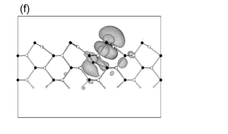
III.2.2 Metastable configuration
As mentioned in Sec. II, there are three inequivalent directions to which the antisite As atom could be displaced to form a - pair. Since the STM experiment Hida et al. (2001) shows that the defect contrasts in the metastable state are all symmetric with respect to the [001] axis, the “up” or “down” configurations could be a candidate for the metastable state. As shown later in Sec. IV, only the “down” configuration gives a better agreement of the calculated STM image with that of experiments. Therefore, only the “down” configuratin is discussed for a possible metastable state of - pairs in this section. When the As antisite is located just on the surface, no metastable configuration is found in simulation.
Figures 5(c)-(f) show the iso-surfaces of the electron density of the highest occupied state when the - pair is formed in the layer 3 and the layer 2. It is notable that the electron density increases exclusively along the direction opposite to the displacement direction of the , which is essentially the same as in the bulk lattice. The iso-surface localized on the and the neighboring three As atoms in the puckered configuration has commonly p-like lobes bonding with each other without nodes as in the bulk lattice. However, the degree of localization of the highest occupied state is slightly dependent on the depth of the atom. When the atom is located in the layer 2 (Figs. 5(e) and 5(f)), the highest occupied state is well localized: The electron density is distributed mainly along the [11] direction. When the is located in the layer 3 (Figs. 5(c) and 5(d)), the electron density is less localized having a distribution over atoms outside the branches. Except for these fine details, the crystal surface has little effect on the electronic structure of the metastable configuration as in the stable one as far as the atom is located below the layer 1.
IV Discussion
IV.1 VALIDITY OF EMBEDDED SYSTEMS
In constructing the atomic configuration, two approximations are employed. First, we relaxed only the atoms in smaller supercell and fixed the lattice constant. The expansion of the lattice constant by the introduce of is 1 %. Staab et al. (2001) It is relatively small in comparison with the change of the distance 6 % between and its nearest neighbor. The atomic configuration around As interstitial is well converged in the system of 65 atoms, Staab et al. (2001) and, therefore, we presume that it is also the case in . Although we actually tried to calculate the electronic structure without the relaxation of the atoms, there remains the features of the electronic structures discussed in Figs. 4 and 5. From these considerations, we conclude that little error is introduced by fixing the lattice constant.
One may consider that the calculated wavefunction could be sensitive to the number of layers. We calculated the electronic structure of the system with smaller surface area and more layers, and found that the essential characteristics of wavefunctions are already converged. Therefore, the electronic structure is not sensitive to the number of layer, or the surface size.
IV.2 SIMULATED STM IMAGES
IV.2.1 STM image in the stable configuration
Figures 6(a), 6(b), and 6(c) show the simulated filled-state STM images of stable atoms in different depths from the surface. The images were calculated by assuming a negative sample bias and hence considering only the iso-surface of the highest occupied state. The image of the in the layer 2 is in good agreement with the previous results. Capaz et al. (1995) As mentioned in Sec. III, even when the is located near the surface, the wavefunction (iso-surface) of the highest occupied state does not differ much from that in the bulk lattice with the characteristic radial pattern. Owing to this fact, when the is located in the layer 2 (Fig. 6(a)), the STM contrast of the defect core arises from the wavefunction concentrated at As atoms in the surface layer (the layer 1) that are neighboring to the , and the satellite contrasts near the core from the wavefunction at the third As neighbors also in the surface layer (the layer 1). When the is located in the layer 3 (Fig. 6(b)), the highest occupied state has a large density on the surface just above the atom and the fifth As neighbors in the surface layer, giving the satellite features. For the located in the layer 4 (Fig. 6(c)), the satellite peaks arise from the seventh As neighbors. Thus, since the satellite peaks originate in the radial pattern of the iso-surface of the highest occupied state, they become more remote from the core contrast with increasing depth of the from the surface.
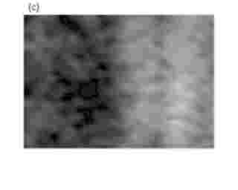
Feenstra et al. Feenstra et al. (1993) argued (later referred to as FWP) that the defect in the STM contrast in their largest size (type A) should be assigned to an in the layer 1, the defect in the second size (type B) to one in the layer 2, the third size (type C) to one in the layer 3, and the fourth size (type D) to one in the layer 4. Their criterion used for judging the depth of the defect was the relative position of surface As atom contrasts with respect to the defect core contrast. Geometrically, if the atom is located in an odd-numbered layer, the mirror symmetric (10) plane passing the atom must cut halfway between As atoms in the surface layer. In contrast, if the is located in an even-numbered layer, the mirror plane must pass an As atom in the surface layer. The assignment by FWP of type B defect as an in the layer 2 agrees with the assignment by Capaz et al. Capaz et al. (1995) As for an in the layer 1, Ebert et al. reported a defect image that is quite different from type A defects by FWP, though such defects were not observed in our experiments probably due to the excessively large magnitude of the bias voltage. Ebert et al. (2001) Figures 6(d) and 6(e) show experimental STM images typically observed at a sample bias of V. Our experimental images shown in Figs. 6(d) and 6(e) seem identical to respectively the type B and C defects in experiments by FWP. Feenstra et al. (1993)
Another criterion for depth assignment is the distance between the two satellites from the core contrast as stated above. The order of the experimental images in Fig. 6 are tentatively arranged according to this criterion. Although the quantitative agreement is not perfect, we could assign the image shown in Fig. 6(e) to an in the layer 3, and image Fig. 6(d) to an in the second layer. The assignment of the type B defect (Fig. 6(d)), the same as proposed by Capaz et al., Capaz et al. (1995) seems reasonable because the agreement of the defect contrast in the metastable state is better than otherwise as shown in what follows.
IV.2.2 STM image in the metastable configuration
Figure 7(c) shows the experimental STM image of the defect in the metastable state that underwent a change from the contrast shown in Fig. 6(e). The image in the metastable state is characterized by the diminish of the satellite peaks and the concomitant appearance of a new contrast elongated along the surface As atom along [110] row on the side opposite to the diminished satellites. As shown in Sec. III, the branches of the radial wavefunction of the highest occupied state disappear upon transformation to the metastable configuration, except for only a branch extending in the [111] direction opposite to the displacement of the atoms. This means that if the atom near the surface was displaced to a “side” position, the STM image would lose the mirror symmetry about the (110) plane. If the atom was displaced to the “up” position, the peak position move in the opposite direction to the one experimentally observed. Both of these contradict the experiments. Hida et al. (2001)
This conclusion is different from the calculations by Zhang, Zhang (1999) where the “side” configuration in the second layer is the most stable energetically among three possible configurations of the metastable state. Our calculation shows the similar energy barrier in the path of from the metastable to the stable positions in these configurations. The energy barrier heights are 0.5 eV in the “side” configuration in the second layer, 0.3 eV in the “down” configuration in the second layer (Fig. 7(a)), and 0.3 eV in the “down” configuration in the third layer (Fig. 7(b)). Therefore, it is still a open question why only one metastable defect image has been observed in STM experiment that is not energetically favorable.
Figures 7(a) and 7(b) show the simulated STM images of - pairs located in the layer 2 and in the layer 3, respectively, with the in the “down” configuration. The agreement between simulation and experiment is better if the is assumed to be located in the layer 3 as tentatively assigned above.
IV.3 Origin of metastability
The physical origin of the metastability of - pairs can be understood if one examines the change in the bonding character upon the stable to metastable transformation. As shown in Sec. III, the configuration, though lower in total energy, bears an inherent instability due to the anti-bonding nature of the chemical bonds with the surrounding atoms. The global expansion of the lattice by the presence of defects is, thus, owing to this anti-bonding nature of the electronic structure associated with the defects. Staab et al. (2001) On transformation to the metastable state, the electronic energy of the s-orbital associated with the atom that is anti-bonded with the nearest As atoms is lifted and becomes emptied. In its place, a gap state associated with an atomic orbital of p-character originating in the displaced As atom is drawn from the conduction band, and it becomes occupied to form bonds with three neighboring As atoms. Thus, some of the increase of the total energy on transformation is canceled by the newly formed chemical bonds which contributes to the affinity of the interstitial As atom with the surrounding.
Since the energy gain by such bond reconstruction should become larger with decreasing distance between the atoms, the change of the dominant orbital of the from s to p-orbital, and the disappearance of the anti-bonding node between and the surrounding As atoms approached by are considered to be the reasons why the metastable state exists.
IV.4 As antisite in (110) surface
As shown in Figs. 4 and 5, the presence of surface has no significant effects on the electronic structures associated with defects as far as they are located deeper than the layer 2. It is only when the is located in the surface layer (the layer 1) that no level is formed in the band gap. Due to the absence of the gap state or the spatial spread of the occupied states, defects in the layer 1 give rise to no localized STM contrast at negative sample biases, in agreement with the results obtained by Ebert et al. Ebert et al. (2001)
The surface buckling Alves et al. (1991) which is reproduced in the present calculation as well is induced by the electron transfer in the Ga dangling bond which is higher in energy to the As dangling bond. This causes a change of the orbital character from in the perfect lattice to -like on the surface Ga atom and to -like on the surface As atom, thereby resulting in the retraction of the Ga atom and the protrusion of the As atom from the surface. Concomitantly, the As dangling bond state smears into the valence band, and the Ga dangling bond state into the conduction bands. It is expected that when defect is located in the surface (layer 1), reverts to the unbuckling position as noticed in a figure of the paper by Ebert et al. Ebert et al. (2001)
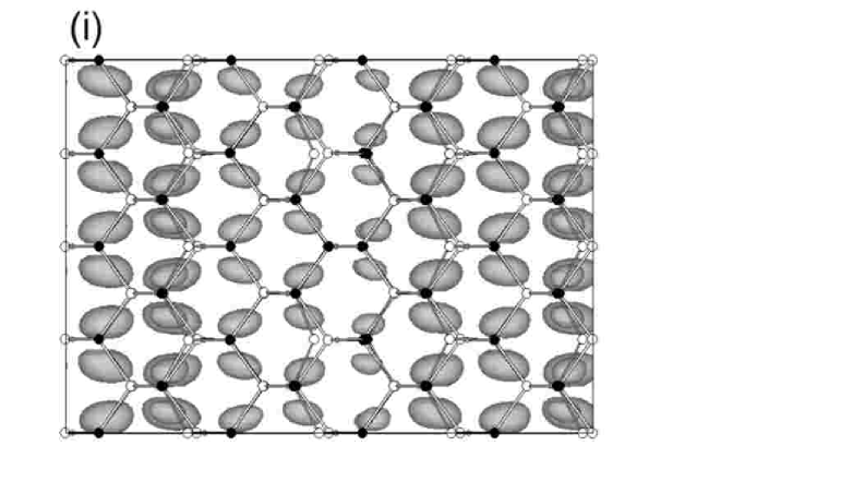
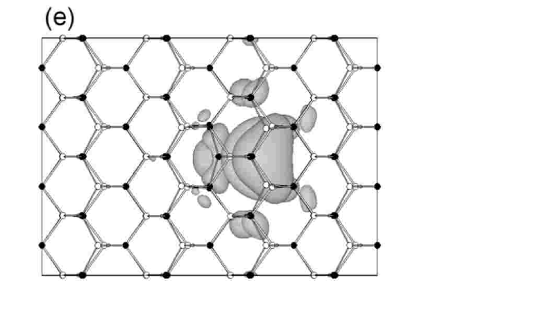
To test this idea, we calculated a model system of 60 atoms with the surface size and with 5 layers including the hydrogen layer by the LMTO method. This model had a clean (110) surface on one end, and the other surface was terminated by hydrogens. Then, was positioned at the same height of As atoms in the surface layer. Figures 8 shows the DOS at the As atom in the surface layer next to the (a) and As atoms distant from the (b). The height of the DOS just below the Fermi energy (between eV and ) is quite different; As atoms in the surface layer away from contain electrons more than an As atom next to . This means that the electrons on the As atoms next to in the surface layer transfer into .
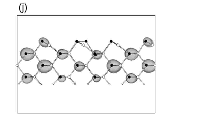
Atoms in the surface layer align in one-dimensional zigzag chains, but each chain does not connect with adjacent chains. Figure 9(a) shows the iso-surface of the highest occupied state which is extended over the whole system with the major component along the [10] chain of surface As atoms next to the [10] chain containing the . The large electron density on this chain originates mainly in the dangling bond orbitals of the As atoms. The much smaller but some density on the is due to the dangling bond p-orbital of the atom. The electron density on the other As atoms in the [10] surface chain containing the does not originate in the dangling bond but in the As p-orbitals parallel to the dangling p-orbital of the . In contrast to the highest occupied states, the lowest unoccupied state (Fig. 9(b)) is localized around the . The iso-surface consists mainly of the dangling bonds of the and the As atoms in the chain containing the . In other words, the dangling bond orbitals of the As atoms are occupied when is absent in the zigzag chain, and are unoccupied when is present in the chain. This means that electrons transferring to are those occupying the dangling bond orbitals of As atoms next to in the surface in case of the perfect lattice. When located in the surface layer, electron transfer does not occur because the energy of dangling bond orbital of As is almost the same as that of and the buckling does not stabilize the state of the electron transfer. Thus, the surface buckling on the site of in the surface layer does not take place.
V Conclusion
We presented the electronic structures of the gap state associated with a single in GaAs. The wavefunction in the stable configuration mainly consists of the s-orbital of and the p-orbitals of the surrounding As atoms. These p-orbitals spread around with a radial pattern of aligned of As p-orbitals. On the other hand, in the metastable configuration, the major component of the wavefunction is the p-orbital of the and the As atoms around it. In comparison with the stable configuration, some p-orbitals of the first neighbor As atoms changes their heading directions breaking the radial pattern of the alignment of the As p-orbitals. As a result, a small part of the radial pattern in the stable configuration remains. These transitions of the orbital and the bonding character can be regarded as the origin of the metastability. These essential features of electronic structures do not change even when the is located near the surface. However, when the is located just on the surface, the surface unbuckles leaving no localized state around the top of the valence band. We can attribute the defect image in the STM experiments to these wavefunction, and the disappearance of the satellite peaks of the images to the change in the wavefunction accompanied by the change to the metastable state. Although they does not thoroughly support experimental results, the results of the present calculations provide simple and clear explanation for the origins of the metastability and the characteristic defect images in the STM experiments.
ACKNOWLEDGEMENTS
This work was supported partially by a Grant-in-Aid for Priority Area on “Manipulation of Atoms and Molecules by Electronic Excitation” from the Ministry of Education, Culture, Sports, Science and Technology (MEXT) of Japan.
References
- Kamińska and Weber (1993) M. Kamińska and E. R. Weber, Imperfections in III/V Materials (Academic Press, San Diego, 1993).
- Martin (1981) G. M. Martin, Appl. Phys. Lett. 39, 747 (1981).
- Fischer (1987) D. W. Fischer, Appl. Phys. Lett. 50, 1751 (1987).
- Chadi and Chang (1988) D. J. Chadi and K. J. Chang, Phys. Rev. Lett. 60, 2187 (1988).
- Dabrowski and Scheffler (1988) J. Dabrowski and M. Scheffler, Phys. Rev. Lett. 60, 2183 (1988).
- Trautman and Baranowski (1992) P. Trautman and J. M. Baranowski, Phys. Rev. Lett. 69, 664 (1992).
- Omling et al. (1986) P. Omling, E. R. Weber, and L. Samuelson, Phys. Rev. B 33, 5880 (1986).
- Manasreh et al. (1990) M. O. Manasreh, D. C. Look, K. R. Evans, and C. E. Stutz, Phys. Rev. B 41, 10272 (1990).
- Taniguchi and Ikoma (1983) M. Taniguchi and T. Ikoma, J. Appl. Phys. 54, 6448 (1983).
- Feenstra et al. (1993) R. M. Feenstra, J. M. Woodall, and G. D. Pettit, Phys. Rev. Lett. 71, 1176 (1993).
- Hida et al. (2001) A. Hida, Y. Mera, and K. Maeda, Physica B 308-310, 738 (2001).
- Capaz et al. (1995) R. B. Capaz, K. Cho, and J. D. Joannopoulos, Phys. Rev. Lett. 75, 1811 (1995).
- Zhang (1999) S. B. Zhang, Phys. Rev. B 60, 4462 (1999).
- (14) Although a calculation was done by Zhang Zhang (1999) for the - pair as the defect in the metastable state, the bias polarity was opposite to that used in the experiments Hida et al. (2001).
- Bonapasta and Giannozzi (2000) A. A. Bonapasta and P. Giannozzi, Phys. Rev. Lett. 84, 3923 (2000).
- Troullier and Martins (1991) N. Troullier and J. L. Martins, Phys. Rev. B 43, 1993 (1991).
- Andersen and Jepsen (1984) O. K. Andersen and O. Jepsen, Phys. Rev. Lett. 53, 2571 (1984).
- Kaxiras and Pandey (1989) E. Kaxiras and K. C. Pandey, Phys. Rev. B 40, 8020 (1989).
- Dabrowski and Scheffler (1989) J. Dabrowski and M. Scheffler, Phys. Rev. B 40, 10391 (1989).
- Tersoff and Hamann (1985) J. Tersoff and D. R. Hamann, Phys. Rev. B 31, 805 (1985).
- Zhang and Northrup (1991) S. B. Zhang and J. E. Northrup, Phys. Rev. Lett. 67, 2339 (1991).
- Schick et al. (2002) J. T. Schick, C. G. Morgan, and P. Papoulias, Phys. Rev. B 66, 195302 (2002).
- Staab et al. (2001) T. E. M. Staab, R. M. Nieminen, J. Gebauer, R. Krause-Rehberg, M. Luysberg, M.Haugk, and T. Frauenheim, Phys. Rev. Lett. 87, 45504 (2001).
- Ebert et al. (2001) P. Ebert, P. Quadbeck, K. Urban, B. Henninger, K. Horn, G. Schwarz, J. Neugebauer, and M. Scheffler, Appl. Phys. Lett. 79, 2877 (2001).
- Alves et al. (1991) J. L. A. Alves, J. Hebenstreit, and M. Scheffler, Phys. Rev. B 44, 6188 (1991).