Organic Single-Crystal Field-Effect Transistors
Abstract
We present an overview of recent studies of the charge transport in the field effect transistors on the surface of single crystals of organic low-molecular-weight materials. We first discuss in detail the technological progress that has made these investigations possible. Particular attention is devoted to the growth and characterization of single crystals of organic materials and to different techniques that have been developed for device fabrication. We then concentrate on the measurements of the electrical characteristics. In most cases, these characteristics are highly reproducible and demonstrate the quality of the single crystal transistors. Particularly noticeable are the small sub-threshold slope, the non-monotonic temperature dependence of the mobility, and its weak dependence on the gate voltage. In the best rubrene transistors, room-temperature values of as high as 15 cm2/Vs have been observed. This represents an order-of-magnitude increase with respect to the highest mobility previously reported for organic thin film transistors. In addition, the highest-quality single-crystal devices exhibit a significant anisotropy of the conduction properties with respect to the crystallographic direction. These observations indicate that the field effect transistors fabricated on single crystals are suitable for the study of the intrinsic electronic properties of organic molecular semiconductors. We conclude by indicating some directions in which near-future work should focus to progress further in this rapidly evolving area of research.
pacs:
71.20.Rv, 72.80.Le, 73.40.QvI Introduction
The electronic properties of Van-der-Waals-bonded organic semiconductors are profoundly different from those of covalently/ionically-bonded inorganic semiconductors Silinsh94 ; Pope99 . In the highly-polarizable crystal lattices of organic semiconductors, the electron-phonon coupling is usually strong and the inter-molecular hopping amplitude small. This results in the formation of self-trapped states with a size comparable to the lattice constant, i.e., the small polarons. The electronic, molecular and lattice polarization plays a key role in determining transport in organic materials, as polaronic effects ”shape” both the dc transport and optical properties of these materials. Because of a very complicated character of the many-particle interactions involved in polaron formation, this problem has been treated mainly at the phenomenological level (see Chapter 7 in Ref. Silinsh94 ). Many basic aspects of this problem have not been addressed yet, and a well-developed microscopic description of the charge transport in organic materials is still lacking.
Until recently, the experimental study of the low-frequency intrinsic electronic properties of organic semiconductors have been performed only on bulk ultra-pure crystals Grosso01 ; Karl80 . In the time-of-flight (TOF) experiments by the group of Norbert Karl at Stuttgart University Karl85 ; Karl99 , it has been found that the mobility of non-equilibrium carriers generated by light absorption in ultra-high-purity oligomeric crystals can be as high as 400 cm2/Vs at low temperatures (the latter value is comparable to the mobility of electrons in Si MOSFETs at room temperature). This behavior suggests that coherent, band-like polaronic transport is possible in crystal of small organic molecules.
To further investigate the electronic properties of organic materials, it is important to go beyond the TOF measurements. One of the alternative techniques to probe the charge transport on a semiconductor surface is based on the electric field effect Sze81 . Continuous tuning of the charge density induced by the transverse electric field enables the systematic study of charge transport, in particular the regime of large carrier density that cannot be accessed in the TOF experiments. The field effect forms the basis for operation of silicon field-effect transistors (FETs), the workhorses of modern inorganic electronics. The field-effect technique is also becoming increasingly popular in the fundamental studies as a convenient method to control the behavior of strongly correlated electron systems such as high-temperature superconductors (see, e.g., Fiory90 ) and colossal magnetoresistance manganites Mathews97 . Other recent examples of applications of this remarkably simple and very successful principle are the electric-field tuning of the metal-insulator transition in cuprates Newns98 and vanadium oxides Kim03 , and the electrostatic control of ferromagnetism in Mn-doped GaAs Ohno00 .
Organic semiconductors are, in principle, well suited for the field-effect experiments. Owing to the weak van-der-Waals bonding, the surface of organic semiconductors (e.g., polyacenes Horowitz98 ; Katz00 and conjugated polymers Bao96 ) is characterized by an intrinsically low density of dangling bonds that can act as the charge traps, and, hence, by a low threshold for the field effect. This fact is at the origin of the rapid progress of organic field-effect transistors based on thin film technology, i.e., organic thin-film transistors (OTFTs) Deleeuw00 ; Dimitrakopoulos02 .
Unfortunately, thin-film transistors are not suitable for the study of intrinsic electronic properties of organic conductors, because their characteristics are often strongly affected by imperfections of the film structure and by insufficient purity of organic materials (see, e.g., Dimitrakopoulos02 ; Horowitz03 ; Campbell01 ). As a consequence, these devices commonly exhibit an exponential decrease of the mobility of field-induced charge carriers with lowering temperature Vissenberg98 . This behavior contrasts sharply a rapid increase of with decreasing temperature, observed in the TOF experiments with bulk ultra-pure organic crystals Karl85 ; Karl99 . Because of a very strong dependence of the OTFT parameters on fabrication conditions, some researchers came to a pessimistic conclusion that even the best organic TFTs ”may not be appropriate vehicles for illuminating basic transport mechanisms in organic materials” Nelson98 .
To explore the intrinsic electronic properties of organic materials and the physical limitations on the performance of organic FETs, devices based on single-crystals of organic semiconductors are needed, similar to the single-crystal structures of inorganic electronics. One of the major impediments to realization of the single-crystal OFETs is the lack of hetero-epitaxial growth technique for the Van-der-Waals-bonded organic films. In this situation, the only viable option to study the intrinsic charge transport on the surface of organic semiconductors is to fabricate the field-effect structures on the surface of free-standing organic molecular crystals (OMCs). However, fabrication of single-crystal OFETs poses a technological challenge. Because the surface of OMCs can be damaged much more easily than that of their inorganic counterparts, organic materials are by and large incompatible with conventional microelectronic processing techniques such as sputtering, photolithography, etc. This is why the systematic investigation of single-crystal OFETs has been carried out only very recently Podzorov03 ; Podzorov03a ; DeBoer03 ; Takeya03 ; Butko03 ; Butko03a , after the successful development of a number of novel fabrication schemes (for earlier work see Horowitz96 ; Ichikawa02 ).
Realization of the single-crystal OFETs opens a new avenue for the study of charge transport in highly ordered molecular systems. The use of single-crystal OFETs as an experimental tool enables the investigation of aspects of charge transport in organic materials that could not be addressed in the TOF experiments. One of the important distinctions between these two types of experiments is the magnitude of carrier densities. Very low densities of charge carriers in the TOF experiments make interactions between them insignificant. At the same time, in the field-effect experiments with organic materials, where accumulation of carrier per molecule seems to be feasible with the use of high-k dielectrics, these interactions could play a major role. Indeed, it is well-known that at a sufficiently high density of chemically-induced carriers, the potassium-doped fullerene KxC60 exhibits superconductivity (x ) and a Mott-Hubbard insulating state (x ) Hebard91 . This example illustrates a great potential of experiments with the single-crystal OFETs.
The first working FET on the surface of a free-standing organic molecular crystal has been fabricated a year ago Podzorov03 . Though this field is in its infancy, the progress has been remarkably rapid, with new record values of carrier mobility for OFETs being achieved, new promising organic materials being introduced, and new device processing techniques being developed. In this review, we discuss the new techniques responsible for the progress, the state-of-the-art characteristics of single-crystal OFETs, and the experiments that show that development of single-crystal OFETs enables investigation of intrinsic electronic properties of organic materials. In the future, the combined efforts of experimenters and theorists, physicists and chemists will be required to reveal the full potential of this research area. We hope that this paper will provide a timely source of information for the researchers who are interested in the progress of this new exciting field.
The structure of this review is as follows. In Section II, we present an overview of the organic crystal growth and techniques for the single-crystal OFET fabrication, with a special attention paid to the crystal characterization. Discussion of the single-crystal OFET characteristics in Section III focuses on revealing the intrinsic transport properties of organic semiconductors. Finally, in Section IV, we summarize the main results, and attempt to predict the directions of rapid growth in this fascinating research field.
II Fabrication of single-crystal organic FETs
The successful realization of FETs on the surface of organic molecular crystals (OMC) is an important milestone in the research of electronic transport in organic semiconductors. For the first time, it opens the opportunity to study the intrinsic behavior of charges at the organic surface, not limited by structural defects. Fabrication of single organic crystal FETs comprises two main steps: the growth of an organic crystal with atomically-flat surface and preparation of the field-effect structure on this surface. In this section we discuss both aspects, paying special attention to the crystal characterization and to the analysis of advantages and limitations of different fabrication methods.
II.1 Single-crystal growth
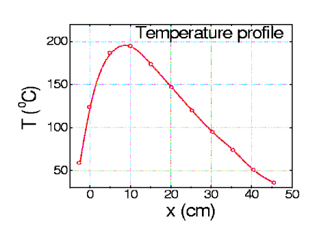
Most of the single crystals used so far for the fabrication of organic FETs have been grown from the vapor phase in a stream of transport gas, in horizontal reactors (glass or, better, quartz tube) Kloc97 ; Laudise98 (for a notable exception, in which the crystals have been grown from solution, see Ref. Mas04 ). In the Physical Vapor Transport (PVT) method, the starting material is placed in the hottest region of the reactor, and the crystal growth occurs within a narrow temperature range near its cold end (see Fig. 1). For better separation of larger and, presumably, purer crystals from the rest of re-deposited material along the tube, the temperature gradient should be sufficiently small (typically, C/cm).
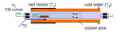
Several ultra-high-purity gases have been used as a carrier agent: in Ref. DeBoer03 , the highest mobility of tetracene-based devices was realized with argon, whereas the best rubrene FETs fabricated so far have been grown in pure H2 Podzorov03 ; Podzorov03a . In the latter case, hydrogen has been chosen after comparison of the field-effect characteristics of rubrene crystals grown in Ar, N2, and H2 atmospheres. It is unclear at present how exactly the transport gas affects the crystal quality; uncontrollable variations of the crystal quality might be caused by the residual water vapor and oxygen in the reactors. Photo-induced reactions with O2 are known for most organic molecules Dabestani96 and the products of these reactions can act as traps for charge carriers. To minimize possible photo-activated oxidation of organic material, the reactors should be pumped down to a reduced pressure mbar prior to the crystal growth, and the growth should be performed in the dark.
Several factors affect the growth process and the quality of the crystals. Important parameters are, for instance, the temperature in the sublimation zone, and the gas flow rate. Many other factors can also play a role: e.g., acoustical vibrations of the reactor in the process of growth might affect the size, shape, and quality of the crystals. For each material and each reactor, the optimal parameters have to be determined empirically. At least in one case (the rubrene-based OFETs Podzorov03a ), it has been verified that the slower the growth process, the higher the field-effect mobility. For this reason, the temperature of sublimated organic material was chosen close to the sublimation threshold. The crystal growth in this regime proceeds by the flow of steps at a very low rate ( cm/s in the direction perpendicular to the a-b plane), and results in a flat surface with a low density of growth steps Laudise70 . As an example, sublimation of 300 mg of starting material in Ref. Podzorov03a took up to 48 hours at C.
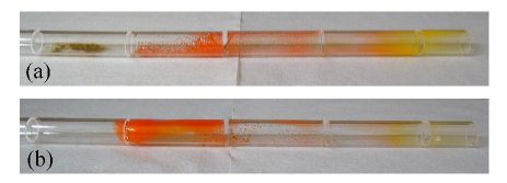
Another important parameter is the purity of the starting material. As the crystal growth process also results in the chemical purification of the material, several re-growth cycles may be required for improving the field-effect mobility, with the grown crystals used as the starting material for the subsequent re-growth. The number of required re-growth cycles depends strongly on the purity of starting material. Figure 2 illustrates the need for several re-growth cycles in the process of the growth of tetracene crystals. Despite the nominal purity of the starting tetracene (Sigma-Aldrich), a large amount of residue left in the sublimation zone after the first growth cycle is clearly visible (Fig. 2a); this residue is not present at the end of the second growth cycle (fig. 2b). A word of caution is appropriate: in the authors’ experience, different batches of as-purchased material, though being of the same nominal purity, might leave different amount of residue. Clearly, the better purity of the starting material, the fewer re-growth cycles are required for a high FET mobility: in Ref. Podzorov03a the rubrene OFETs with cm2/Vs have been fabricated from the ”sublimed grade” material (Sigma-Aldrich) after only growth cycles.
It is likely that the purity of crystals for the OFET fabrication can be substantially improved if a zone refining process Grosso01 ; Karl80 is used for pre-purification of the starting material. Indeed, in the time-of-flight studies of organic crystals, the best results and the highest mobilities have been obtained after multiple zone-refinement purification cycles Karl80 ; Karl85 . This process enabled reduction of the impurity concentration in the bulk down to the part-per-billion level. It is unlikely that a comparable purity can be achieved simply by multiple vapor transport re-growth processes. It has to be noted that zone-refinement cannot be applied to all organic materials, since this technique requires the existence of a coherent liquid phase (i.e. the melting temperature of the substance has to be lower than the temperature of decomposition of its molecules) Grosso01 . However, for several materials that have already been successfully used for fabrication of single crystal FETs (e.g., rubrene, perylene, anthracene), a coherent liquid phase does exist and zone refinement is possible. The zone-refining purification might be especially useful for realization of intrinsic polaronic transport at low temperatures, where trapping of polarons by defects becomes a serious problem.
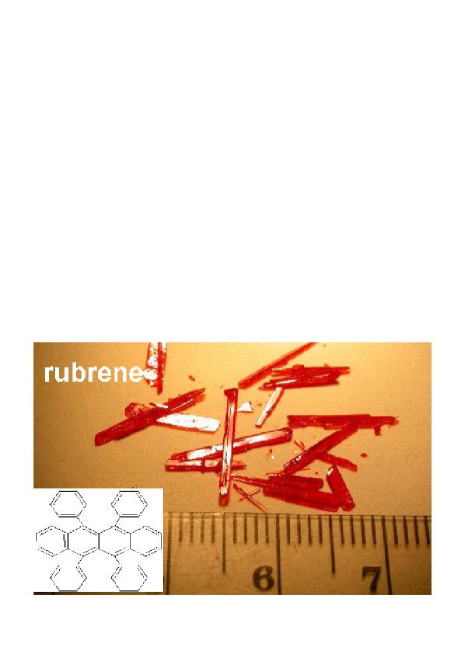
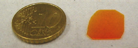
Most of the organic crystals grown by the physical vapor transport are shaped as elongated ”needles” or thin platelets (see Fig. 3). The crystal shape is controlled by the anisotropy of inter-molecular interactions: for many materials, a larger crystal dimension corresponds to the direction of the strongest interactions and, presumably, the strongest overlap between -orbitals of adjacent molecules. For this reason, the direction of the fastest growth of needle-like rubrene crystals coincides with the direction of the highest mobility of field-induced carriers (see Sec. III). For platelet-like crystals, the larger facets are parallel to the a-b plane. Typical in-plane dimensions range from a few square millimeters for rubrene to several square centimeters in the case of anthracene. The crystal thickness also varies over a wide range and, in most cases, can be controlled by stopping the growth process at an early stage. For example, the thickness of the tetracene crystals grown for 24 hours ranges between m and m DeBoer04 , but it is possible to harvest several crystals of sub-micron thickness by stopping the growth process after minutes.
Because of a weak van der Waals bonding between the molecules, polymorphism is a common phenomenon in organic materials: the molecular packing and the shape of organic crystals can be easily affected by the growth conditions. For example, the thiophenes exhibit two different structures depending on the growth temperature Horowitz95 . In many cases, organic molecular crystals exhibit one or more structural phase transitions upon lowering the temperature. For the study of single-crystal FETs at low temperature, the occurrence of a structural phase transition can be detrimental. In tetracene crystals, for instance, a structural phase transition occurs below 200 K (see, e.g., Sondermann85 ). Co-existence of two crystallographic phases at lower temperatures causes the formation of grain boundaries and stress, which are responsible for the trapping of charge carriers (see Fig. 10). In tetracene, in addition, occurrence of the structural phase transition often results in cracking of the crystals with cooling and a consequent device failure.
II.2 Crystal characterization
To understand better the effect of different factors on the crystal growth, a thorough characterization of the crystal properties is needed. Note, however, that many experiments provide information on the crystal properties that is only indirectly related to the performance of the single-crystal OFETs. For example, the x-ray analysis of organic crystals, though necessary for identification of the crystal structure and orientation of the crystallographic axes, is insufficiently sensitive for detection of a minute concentration of defects that might severely limit the field-effect mobility at low temperatures. Similarly, the TOF experiments, although useful in assessing the quality of the bulk of organic crystals, are not sensitive to the surface defects that limit the OFET performance. Below we briefly review several techniques that have been used for organic crystal characterization.
II.2.1 Polarized-light microscopy
Inspection of crystals under an optical microscope in the polarized light provides a fast and useful analysis of the crystalline domain structure. Visualization of domains is possible because crystals of most organic conjugated materials are birefringent Vrijmoeth98 . Optical inspection also enables detection of the stress in crystals, which results in appearance of the interference fringes with orientation not related to any specific crystallographic direction. This technique simplifies the process of selection of single crystals for transport measurements.
II.2.2 The time-of-flight experiments
In the time-of-flight (TOF) experiments, a platelet-like crystal is flanked between two metal electrodes, one of which is semi-transparent Karl85 . A thin sheet of photo-excited charge carriers is generated near the semi-transparent electrode by a short laser pulse with the photon energy greater than the band gap. In the presence of a constant voltage bias between the two electrodes, the charge sheet propagates in the direction determined by the dc electric field and generates a displacement current, whose magnitude diminishes rapidly as soon as the sheet reaches the opposite electrode Grosso01 . From the duration of the displacement current pulse and the known crystal thickness, the drift velocity and carrier mobility can be calculated. This method also provides indirect information on the concentration of (shallow) traps in the bulk: the decrease of mobility at low temperatures is caused by multiple trapping and release processes (for more details, see Ref. Hoesterey63 ). An important aspect of TOF measurements is that their results are not sensitive to contact effects, since the charge carriers are photo-generated (i.e., not injected from a metal electrode) and their motion is detected capacitively. This simplifies the contact preparation and improves the reproducibility of results for identically grown crystals.
For measuring the intrinsic mobility of charge carriers in the bulk, the lifetime of the carriers against charge trapping has to be greater than the time of flight between the electrodes. This requirement imposes severe limitation on the concentration of charge traps. As a result, only very pure and defect-free crystals can be characterized by the TOF method. For example, according to preliminary measurements by the Stuttgart group Stuttgart04 , the rubrene crystals used for fabrication of the high-mobility OFETs Podzorov03a are unsuitable for the TOF measurements. The crystals for the TOF measurements should also have sufficiently parallel opposite facets and be sufficiently thick for the displacement current pulse to be longer than the apparatus time resolution. Because of these limitations, the TOF measurements can be performed only on a small fraction of the crystals grown by the phase vapor deposition technique.
Despite the difficulties of application of the TOF method to the organic crystal grown by vapor transport, successful TOF measurements have been performed on vapor-grown tetracene crystals similar to those used in FETs experiments DeBoer04 . The room-temperature mobility cm2/Vs, measured in the TOF experiment for three different crystals, is comparable to the highest mobility of the field-induced carriers in the OFET experiments; these quantities also exhibit similar temperature dependencies. Interestingly, the two types of measurements provided similar values for charge transport along different directions in anisotropic organic crystals: the FET measurements probe surface transport in the a-b plane, whereas TOF experiments on the platelet tetracene crystals probed motion along the c-axis. This observation seems to be in disagreement with what one would expect from the crystallographic structure of the material, namely a pronounced anisotropy of mobility along different crystallographic directions Karl99 ; Karl85a ; Karl01 . To better understand the origin and the implications of this result, further characterization of a larger variety of organic crystals by the TOF method and comparison with field-effect measurements are needed.
II.2.3 Space charge limited current spectroscopy
A rather common and, in principle, simple way to characterize the electrical properties of OMCs is the study of the characteristics measured in the space charge limited current (SCLC) regime Lampert70 . The value of the carrier mobility, as well as the density of deep traps can be inferred from these measurements. Similar to the TOF experiments, SCLC measurements require relatively large electric fields. Usually, these measurements are performed on thin platelet-like crystals; the metallic contacts are located on the opposite facets of a crystal of thickness , and the current in the direction perpendicular to the surface (along the c-axis) is measured as a function of the voltage between the contacts. Measurements of characteristics with contacts on the same surface of the crystal can also be performed, but in this geometry the extraction of the carrier mobility and the density of traps from the experimental data is more involved. Instrumentation-wise, the dc charge injection experiments are less challenging than the TOF measurements. However, a high quality of contacts is required for the former measurements, otherwise the results for nominally identical samples are not reproducible DeBoer04 . Because of a high sensitivity of the data to the contact quality, the SCLC technique typically requires acquisition of a large volume of data for many samples and, therefore, is not very efficient.
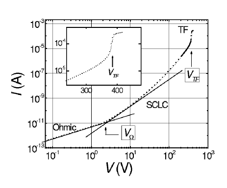
Recently, the trap-free space charge limited current (SCLC) regime has been observed for samples with both thermally-evaporated thin-film contacts Podzorov03a and silver epoxy contacts DeBoer04 . The characteristics for a thin rubrene crystal with thin-film silver contacts demonstrate the crossovers from the Ohmic regime to the space-charge-limited-current (SCLC) regime, and, with a further voltage increase, to the trap-free (TF) regime (see Fig. 7) Podzorov03a . Observation of a linear Ohmic regime indicates that the non-linear contribution of Schottky barriers formed at the metal/rubrene interfaces is negligible in these measurements: the voltage drop across the Schottky barriers is smaller than the voltage drop across the highly resistive bulk of the crystal. The crossover to the SCLC regime at a low bias voltage V suggests that the charge carrier injection from the contacts is very efficient. From the threshold voltage of the TF regime, , the density of deep traps, , can been estimated Lampert70 ; Kao81 :
| (1) |
Here is the permittivity of free space, is the relative dielectric constant of the material. Note that an assumption-free estimate of the trap density can be made only if a well-defined crossover between SCLC and TF regimes is observed. For this reason, the method can be applied only to sufficiently pure crystals. For the tetracene crystals studied in Ref. DeBoer04 , cm-3 is significantly smaller than cm-3 for rubrene crystals studied in Ref. Podzorov03a . The steep increase of current that signifies the transition to the trap-free regime, is also much more pronounced for tetracene crystals (see Fig. 7 and 8).
The estimate of is based on the assumption (not usually mentioned in the literature), that the deep traps are uniformly distributed throughout the entire crystal bulk. However, it is likely that the trap density is greater near the metal/organic interface because of the surface damage during the contact preparation. A small amount of traps located close to the surface can have a large effect on the current flow: the charges trapped near the surface strongly affect the electric field in the bulk of the crystal, which determines the current flow in the TF regime. For this reason, the value of may be considered as an upper limit of the actual density of traps in the bulk (see Ref. DeBoer04 for a more detailed discussion).
In the TF regime, the mobility can be estimated from the Mott-Gurney law for the trap-free regime Lampert70 :
| (2) |
where is the current density. Even when the TF limit is not experimentally accessible, the same formula can be used to extract a lower limit, for the intrinsic mobility, at least in materials in which one type of carriers (electrons or holes) is responsible for charge transport (see Ref. DeBoer04 for details). In tetracene crystals, the values of along the c-axis obtained from SCLC measurements performed on a large number of samples are shown in Fig. 9. The large spread in values for obtained from identically grown crystals is due to scattering in the contact parameters.
For the samples with cm2/Vs, the mobility increases with cooling over the interval K (Fig. 10). Observation of the mobility increase with cooling in high-quality crystals is usually considered as a signature of the intrinsic (disorder-free) transport (for comparison, an increase of mobility with lowering temperature has never been observed in SCLC measurements performed on disordered thin organic films). With further cooling, however, the mobility decreases: Fig. 10 shows that for most of the tetracene crystals, a sharp drop of below 180 K is observed. This suggests that this drop might be related to a structural phase transition, which is known to occur in tetracene in this temperature range Sondermann85 . Both the observed effects of the structural phase transition on the carrier mobility, as well as the increase in with lowering temperature, indicate that these SCLC measurements reflect the intrinsic electronic properties of the material.
II.3 Fabrication of the field-effect structures
Fabrication of the field-effect structure on the surface of organic crystals poses a challenge, because many conventional fabrication processes irreversibly damage the surface of van-der-Waals-bonded organic crystals by disrupting molecular order, generating interfacial trapping sites, and creating barriers to charge injection. For example, sputtering of an insulator onto the crystal creates such a high density of defects on the organic surface that the field-effect is completely suppressed. Up to date, two techniques for single-crystal OFET fabrication have been successfully used: (a) electrostatic ”bonding” of an organic crystal to a prefabricated source/drain/gate structure, and (b) direct deposition of the contacts and gate insulator onto the crystal surface. In this section, we address the technical aspects of these fabrication processes; effect of different fabrication methods on the electrical characteristics of the resulting single-crystal FETs will be discussed in Sec. III.
II.3.1 Electrostatic bonding technique
In this approach, the transistor circuitry (both gate and source/drain electrodes) is fabricated on a separate substrate, which, at the final fabrication stage, is electrostatically bonded to the surface of organic crystal. The technological processes vary depending on the type of a substrate for the transistor circuitry. Two kinds of substrates have been used: conventional silicon wafers DeBoer03 ; Takeya03 ; Ichikawa02 , and flexible elastomer substrates (the so-called rubber stamps) Rogers03 .
Source/drain/gate structures on Si substrates
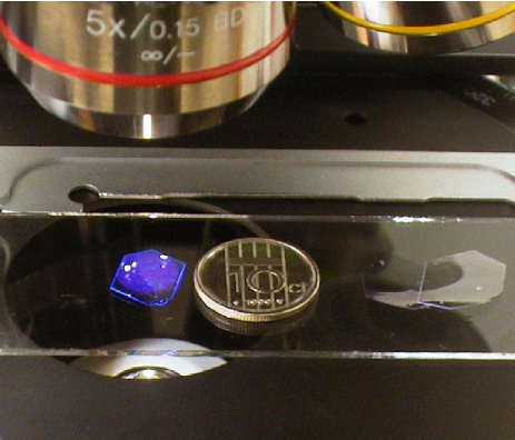
In this method, the source/drain/gate structure is fabricated on the surface of a heavily doped (n-type or p-type) Si wafer, covered with a layer of thermally grown SiO2 (typically, m thick). The conducting Si wafer serves as the gate electrode, and the SiO2 layer plays the role of the gate insulator. The source and drain gold contacts are deposited on top of the SiO2 layer, and, as a final step, a sufficiently thin OMC crystal is electrostatically bonded to the source/drain/gate structure. It has been found in Ref. DeBoer03 that the reactive ion etching (RIE) of the contact/SiO2 surface in the oxygen plasma prior to the OMC bonding improves significantly the characteristics of tetracene OFETs: the RIE cleaning reduces the spread of mobilities, the field-effect threshold voltage, and the hysteresis of transfer characteristics. The RIE cleaning also significantly improves adhesion of freshly grown tetracene crystals to SiO2 surface. The technique works best for very thin crystals (m thick) that adhere spontaneously to the substrate, but it can also be applied (with a lower success yield) to much thicker crystals by gently pressing on the crystal to assist the adhesion process Jurchescu03 . Fig. 11 shows a picture of a rubrene FET fabricated with the technique of electrostatic adhesion to SiO2.
Source/drain/gate structures on flexible substrates
In this approach, the FET circuitry is fabricated on top of a flexible elastomer substrate (polydimethylsiloxane, or PDMS), by sequential shadow-mask deposition of the gate and source/drain electrodes Rogers03 . The fabrication process, illustrated in Fig. 12, begins with deposition of the gate electrode on top of a few-mm-thick PDMS substrate (1.5 nm of Ti as an adhesion promoter to the substrate, 20 nm of Au, and 3 nm of Ti as an adhesion promoter to the subsequent layers). A (2-4)m-thick PDMS film, deposited by spin-coating on top of the structure, serves as a gate dielectric. Evaporation or transfer printing of source and drain electrodes (1.5 nm of Ti and 20 nm of Au) on top of the dielectric completes the stamps. Careful control of the fabrication processes results in electrode and dielectric surfaces with low surface roughness (the root-mean-squared value of nm, as measured by atomic force microscopy). The final assembly of the devices, similar to the Si-based technique, consists of positioning of the OMC crystal on the stamp surface, and applying a gentle pressure to one edge of the crystal. Van der Waals forces then spontaneously cause a ”wetting” front to proceed across the crystal surface at a rate of a few tenths of a millimeter per second. This lamination process yields uniform contact, devoid of air gaps, bubbles or interference fringes.
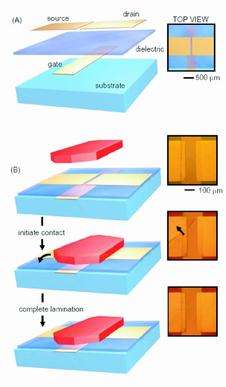
The main advantage of both Si- and PDMS-based stamps technique is obvious: it eliminates the need for deposition of metals and dielectrics directly onto a very vulnerable organic surface. Since these techniques exploit the technologies well-developed in electronic industry, the dimension of the circuitry can be easily reduced, if desirable, well in the sub-micron range: specifically, a very small source/drain contact separation can be achieved by using electron-beam lithography. The PDMS-based masks work well not only for thin, but also for thick crystals: the flexible PDMS surface and the ductile Au contacts adjust easily to the crystal shape (i.e. no flexibility of the crystal is required). Remarkably, despite the fact that rubbers become rigid upon cooling, this technique has been shown to work well at low temperatures Sundar04 . Another important advantage of the PDMS stamp technique is that it is non-destructive and reversible: it has been shown that the contact between the stamp and the rubrene crystal can be re-established many times without noticeable degradation of the OMC surface Rogers03 . For this reason, PDMS-supported circuitry has been used for the first observation of the anisotropy of the field-effect mobility within the a-b plane of the single crystals of rubrene, as we discuss in Sec. III.6. Interestingly, simple adhesion of organic crystals to metallic surface results in contacts with good electrical properties. This has been demonstrated for both Si- and PDMS- based stamps by comparing the results of two- and four-probe measurements. The contact resistance is similar to that observed in the devices for which the thin metal film contacts are directly deposited onto the organic surface (see below).
Although its simplicity makes electrostatic bonding particularly appealing for the fabrication of organic single crystal FETs, this technique also suffers from a number of limitations. For instance, the choice of metals for the source and drain contacts in the electrostatic ”bonding” technique is limited by noble metals, since other materials are easily oxidized in air. The channel width is not well defined (unless it is limited by the crystal dimensions or by patterning the gate electrode), because the conduction channel is formed over the whole area of overlap between the OMC crystal and the Si wafer. In the current PDMS-stamp OFETs, the gate insulator is relatively thick and its dielectric constant is low - for this reason, the maximum density of induced charges is relatively small (typically, below carriers/cm2). Finally, another potential problem of the Si- and PDMS stamps might be the mismatch between the coefficients of thermal expansion for the stamp and the organic crystal. Upon changing the temperature, this mismatch might cause a mechanical stress and formation of defects in the crystal. Since the surface defects can trap the field-induced charge, this might result in deterioration of the low-temperature OFET characteristics. This is an important issue that requires further studies.
OFETs with high-k dielectrics
The electrostatic bonding technique is compatible with the use of high-k dielectrics as gate insulators, which allow the accumulation of a large carrier density in OFETs. Particularly interesting is the possibility of reaching a surface charge density of the order of carriers/cm2, which corresponds to approximately one charge carrier per molecule (this estimate assumes that all the charges are accumulated in a single molecular layer, as it is expected from calculations of the screening length). Indeed, the maximum surface charge density is , where is the relative dielectric constant of the gate dielectric and is its breakdown field. For typical high-k dielectrics, such as Ta2O5 or ZrO2, and MV/cm, and the resulting charge density at the breakdown is carriers/cm2. Many novel high-k materials hold the promise of even higher charge densities Dover98 ; Ren01 .
The process of fabrication of OFETs with high-k dielectrics is similar to the aforementioned Si-based technique, with SiO2 replaced by a high-k dielectric that is sputtered onto a heavily doped silicon substrate. In the experiments at TU Delft, Ta2O5 and ZrO2 gate dielectrics have been sputtered onto the Si wafers at room temperature. Though the measured values of the dielectric constant and breakdown field for these layers are close to the best results reported in literature Fleming00 , the leakage currents were relatively large ( A/cm2 for a Ta2O5-thickness of 350 nm). This is typical for deposition of dielectric films onto non-heated substrates, which results in a relatively high density of vacancies in the films. Substantially lower values of the leakage currents might be achieved in the future by sputtering on heated substrates, as already demonstrated in literature Fleming00 . The characteristics of tetracene single-crystal FETs with high-k dielectrics will be discussed in Sec. III.
II.3.2 ”Direct” FET fabrication on the crystal surface
The ”direct” fabrication of the single-crystal OFETs, in which a free-standing OMC is used as the substrate for subsequent deposition of the contacts and gate dielectric, is not trivial, because the organic crystals are incompatible with the standard processes of thin-film deposition/patterning. Fabrication of the field-effect structures based on single crystals of organic semiconductors became possible after several innovations have been introduced both for the source/drain fabrication and for the gate dielectric deposition Podzorov03 ; Podzorov03a .
Source/drain contacts
The performance of the organic FETs is often limited by the injection barriers formed at the interface between the metal contacts and the semiconductor. The charge injection in such devices occurs by thermally assisted tunneling of the electrons or holes through the barrier, whose effective thickness depends on both gate and source-drain voltages. This is why reducing of the contact resistance is especially important for proper functioning of OFETs.
Different routes have been followed for the fabrication of source/drain contacts on the surface of organic crystals. The simplest (but also the crudest) is the ”manual” application of a conducting paste. Among the tested materials, the water based solution of colloidal carbon provided the lowest contact resistance to organic crystals. A two-component, solvent-free silver epoxy (Epo-Tek E415G), which hardens at room temperature in a few hours, has been also used DeBoer04 . A disadvantage of this method is that it is difficult to prepare small and nicely-shaped contacts on hydrophobic OMC surfaces. In addition, this technique often results in formation of defects (traps) at the contact/organic interface, as shown, for instance, by the transport experiments in the space charge limited transport regime.
The thermal deposition of metals through a shadow mask is a more versatile method. However, the thermal load on the crystal surface in the deposition process (mostly because of radiation from the evaporation boat) has to be painstakingly minimized: deposition might generate traps at the metal/organic interface, or even result in the OMC sublimation. The effect of fabrication-induced traps has been regularly observed in both FET and SCLC measurements; presence of these traps is also a plausible cause for irreproducibility of the metal contacts evaporated on top of organic films used in applied devices Shen01 ; Liu01 ; Rep03 . This limits the choice of metals to the materials with a relatively low deposition temperature. As a first (and very crude) approximation, matching of the metal work-function to the HOMO(LUMO) levels of OMC for the p-type (n-type) conductivity can be used as the guideline in the metal selection.
Despite the technological difficulties, successful deposition of high-quality silver contacts by thermal evaporation has been recently performed, which demonstrates that the contact fabrication problems are not intrinsic. In order to minimize damage of the crystal surface, the authors of Ref. Podzorov03a fixed the deposition rate at a low level (/s), increased the distance between the evaporation source and the sample up to 70 cm, maintained the crystal temperature during the deposition within the range C by using a Peltier cooler, and placed a diaphragm near the evaporation boat to shield IR radiation from the hottest parts of the boat. It has been also observed that, in order to achieve high mobilities, it is important to avoid contamination of the channel surface by metal atoms deposited at oblique angles under the shadow mask. Such contamination, which dramatically affects the device performance, presumably occurs because of scattering of silver atoms from residual gas molecules even at Torr, the typical pressure in the chamber for contact deposition. In order to prevent oblique angle deposition in the shadowed regions, silver was deposited through a ”collimator”, a narrow (4 mm ID) and long (30 mm) tube, positioned close to the crystal surface. Following this process, high-quality OFETs have been fabricated on the surface of several organic crystals (rubrene, TCNQ, pentacene).
In the future, it would be useful to better understand the mechanism of damaging of organic crystals in the process of contact fabrication, in order to make the preparation of high-quality contacts routinely possible with many different metals. In particular, preparation of high-quality contacts will help to elucidate the role of the work function of the metallic electrodes, which seems to play a less prominent role than what was initially expected (see, e.g., Gao03 ).
Parylene as a novel gate dielectric
After many unsuccessful attempts, it became clear that sputtering of Al2O3, as well as other dielectrics, onto the surface of organic molecular crystals unavoidably results in a very high density of traps and prohibitively high field-effect threshold: the field effect is completely suppressed even if the organic crystals were positioned in the shadow region of the vacuum chamber, where the deposition rate was zero. Presumably, the OMC surface is damaged by high-energy particles in the plasma. The attempts to shield the surface from high-energy charged particles by electrostatic deflection did not improve the situation. Thermal deposition of silicon monoxide was also unsuccessful, probably because of a too high temperature of the deposition source.
The breakthrough in the ”direct” fabrication of free-standing single-crystal OFETs came with using thin polymer films of parylene as a gate-dielectric material Podzorov03 . Parylene coatings are widely used in the packaging applications; the equipment for parylene deposition is inexpensive and easy to build (see, e.g., Parylene Conformal Coatings Specifications and Properties, Technical notes, Specialties Coating Systems). This material with the dielectric constant forms transparent pinhole-free conformal coatings with excellent mechanical and dielectric properties: the breakdown electric field could be as high as MV/cm for the thickness m.
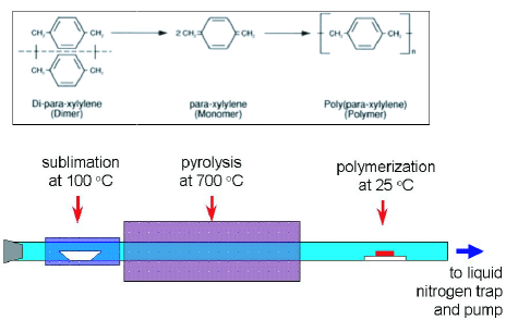
In Ref. Podzorov03 , parylene was deposited in a home-made reactor with three temperature zones (see Fig. 13). Prior to the deposition, the reactor (quartz tube) was evacuated to a pressure of mTorr. The dimer para-xylylene (generic name, parylene) is vaporized in the vaporization zone at C, cleaves in the pyrolysis zone at C, and polymerizes in the deposition zone (the sample location) at room temperature and pressure Torr. The precise value of these parameters during the parylene deposition is not critical. In Ref. Podzorov03 , the parylene deposition rate was /min for the samples positioned cm away from the pyrolysis zone of the parylene reactor. Parylene was deposited onto the OMC crystals with pre-fabricated source and drain contacts with the attached wires (otherwise, contacting the contact pads might be difficult). The parylene thickness m is sufficient to cover uniformly even the rough colloidal-graphite contacts. The capacitance of the gate electrode per unit area, , was nF/cm2 for a -m-thick parylene film. The output of working devices with the parylene gate insulator approached and the parylene films deposited onto organic crystals withstand multiple thermal cycling between 300 K and 4.2 K.
There are several important advantages of using parylene as the gate dielectric: (a) it can be deposited while the crystal remain at room temperature, (b) being chemically inert, it does not react with OMCs, and (c) the parylene/OMC interface has a low density of surface states. Apart from that, parylene is a carbon-based polymer, and its thermal expansion coefficient is likely to be close to that of most organic crystals (but that remains to be tested). As it has already been emphasized above, different thermal expansion/contraction of the crystal and gate dielectric might result in the stress-induced carrier trapping. In this regard, the use of parylene is particularly promising for the operation of OFETs at low temperature. Parylene is also promising as the gate insulator for the future thin-film, flexible devices, where flexibility of the gate dielectric is required.
III Characteristics of single-crystals OFETs
Fabrication of the single-crystal OFETs enables exploration of the physical limits on the performance of organic thin-film FETs. For the first time, one can study the characteristics of OFETs not limited by the disorder common for organic thin films. As the result, many important characteristics of OFETs, including the charge carrier mobility, the field-effect threshold, and the sub-threshold slope, have been significantly improved.
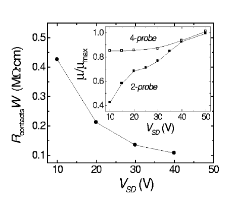
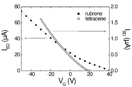
The organic semiconductors used in OFETs are undoped (or, at least, not intentionally doped). For this reason, OFETs belong to the class of injection, or Schottky-limited FETs, in which the charge carriers are injected into the conduction channel through the Schottky barriers at the metal/organic interface. For the same reason, the resistance of source and drain contacts is much higher than in Si MOSFETs, and depends strongly on the biasing regime. Since the contact resistance might be comparable or even greater than the channel resistance (especially at low temperatures), only the 4-probe measurements provide the intrinsic characteristics of the conduction channel, not affected by the contact resistance. However, in the limit of large and , the contact resistance becomes small, and the results of 2-probe and 4-probe measurements typically converge, at least at room temperature (see Fig. 14).
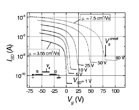
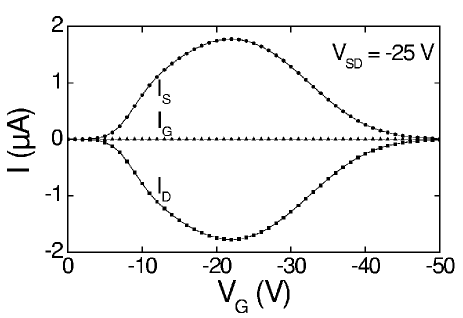
It is worth mentioning that at this initial stage, when the research focuses mostly on the study of the intrinsic field-induced conductivity in organic semiconductors, the biasing regimes in the experiments with single-crystal OFETs often differ from the conventional FET biasing Horowitz98 . The difference is illustrated in Fig. 15: the polarity of the source-drain voltage is chosen to explore a wider range of the carrier densities. Note also that, because single-crystal devices have not been optimized for applications (e.g., the gate insulator is much thicker than in the commercial devices), the typical values of and are an order of magnitude greater than that for the conventional Si MOSFETs. The main characteristics of the single-crystal FETs are summarized below.
III.1 Unipolar operation
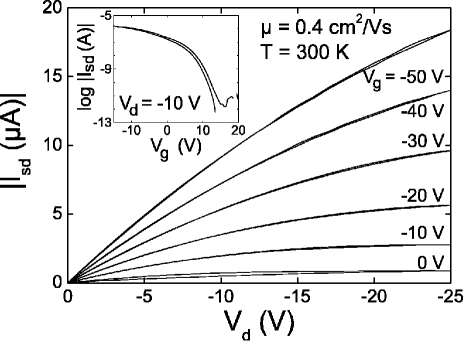
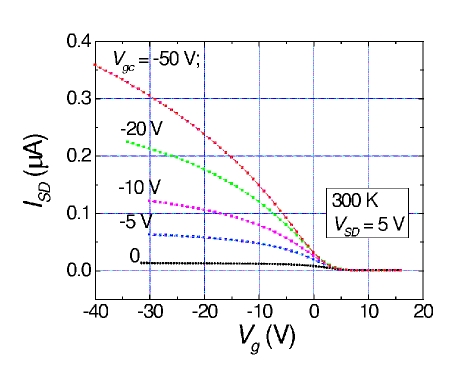
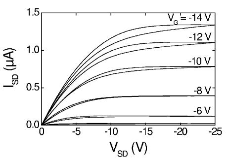
All the single-crystal devices fabricated up to date exhibited unipolar operation. Specifically, the p-type conductivity has been observed, for instance, in antracene, tetracene, pentacene, perylene, rubrene, whereas the n-type conductivity has been observed in TCNQ. Typical transistor characteristics for the rubrene and tetracene single crystal OFETs are shown in Fig. 16 and 17. In principle, the unipolar operation can be explained by the choice of metallic contacts that are efficient injectors of only one type of carriers. However, the presence of traps that selectively capture either electrons or holes cannot be excluded. For instance, the TOF experiments with perylene Karl99 ; Karl85a have shown that in high quality crystals of this compound, both electrons and holes are sufficiently mobile at room temperature. However, in the single-crystal perylene FETs, only the hole conduction has been observed DeBoer03a . One of the reasons for that might be presence of oxygen in the crystal, which is known to act as a trap for electrons.
III.2 Field-effect threshold
The threshold voltage is a measure of the amount of charge that it is necessary to induce electrostatically in order to switch-on electrical conduction in a FET. Using the equation that describes FET operation
| (3) |
can be obtained by extrapolating the quasi-linear (high-) part of trans-conductance characteristics to zero current (here and are the width and the length of the conducting channel, respectively, and is the specific capacitance between the channel and the gate electrode). The charge induced in the sub-threshold regime fills the traps that immobilize the charge carriers.
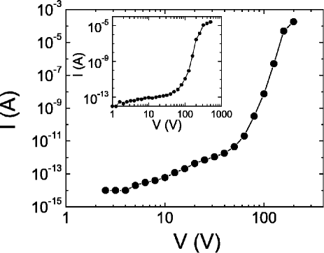
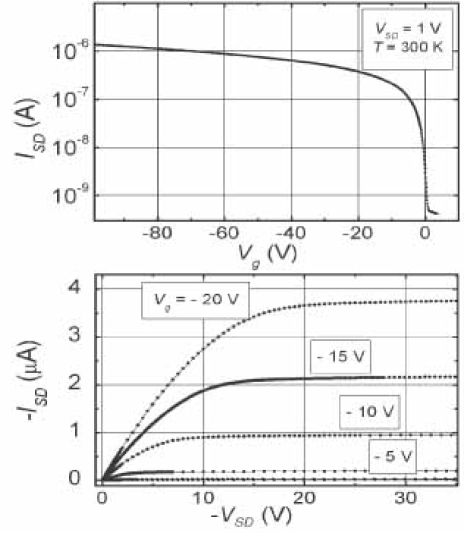
The magnitude of the field-effect threshold voltage depends on several factors, such as the density of charge traps on the interface between the organic crystal and the gate dielectric, the quality of the source/drain contacts (particularly important for Schottky transistors), and the absence/presence of a ”built-in” conduction channel. Firstly, let’s consider the situation when the built-in channel is absent; this is the case, for example, of the rubrene devices with parylene gate dielectric Podzorov03 ; Podzorov03a . The corresponding trans-conductance characteristics are shown in Fig. 15 on a semi-log scale. The field-effect onset is observed at a positive gate voltage, similar to the OFET based on well-ordered pentacene thin-films Nelson98 ; Klauk02 ; Meijer03 . This behavior resembles the operation of a ”normally-ON” p-type FET with a built-in channel. The resemblance, however, is superficial: in Ref. Podzorov03a , the sharp onset was always observed at , which indicates that the channel was induced electrostatically. Indeed, an application of a positive voltage to the source electrode in the presence of the gate electrode m away from the interface creates a strong electric field normal to the crystal surface. This field induces propagation of the conducting channel from the source electrode to the drain at any . Thus, the single-crystal rubrene OFETs with parylene gate dielectric are zero threshold devices at room temperature. The zero threshold operation suggests that the density of the charge traps at the rubrene/parylene interface is low ( cm-2) at room temperature notetraps . However, the situation changes at low temperatures: the threshold voltage, measured in the 4-probe configuration, increases with cooling (see Fig. 23). This might signal depopulation of the surface traps that are filled at room temperature. Note that only the 4-probe measurements are essential to study the behavior of ; in the 2-probe measurements, an increase of the non-linear contact resistance with cooling might imitate the threshold shift.
For the OFETs fabricated by the electrostatic bonding of organic crystals, a relatively large (10 V or more) depletion gate voltage is often required to completely pinch off the channel (this is positive for the p-type conductivity). This behavior is illustrated in Fig. 18 for rubrene and for tetracene crystals bonded to the RIE pre-cleaned SiO2 surface DeBoer03 , similar behavior has been observed for pentacene Takeya03 . The positive threshold has been also observed for the rubrene crystals bonded electrostatically to the surface of PDMS rubber stamps Sundar04 . These observations suggest that the same microscopic mechanism responsible for electrostatic bonding might be responsible for inducing the built-in channel on the organic surface.
III.3 Sub-threshold slope
The sharpness of the field-effect onset is characterized by the sub-threshold slope, . Since this quantity depends on the capacitance of the insulating layer , it is also convenient to introduce the normalized slope, , which permits to compare more directly the properties of different devices Podzorov03a . For single crystal FETs, even in the devices with relatively low mobility (the tetracene single-crystal FETs with cm2/Vs DeBoer03 ), the observed normalized sub-threshold slope VnF/decadecm2 was comparable with that for the best pentacene TFTs ( VnF/decadecm2 Dimitrakopoulos99 ; Lin97 ; Dimitrakopoulos99a ). The high-mobility single-crystal rubrene OFETs with cm2/Vs exhibit a sub-threshold slope as small as V/decade, which corresponds to VnF/decadecm2 Podzorov03a . This value is an order of magnitude better than what has been achieved in the best organic TFTs; it also compares favorably with -Si:H FETs, for which VnF/decadecm2 has been reported Kanicki91 .
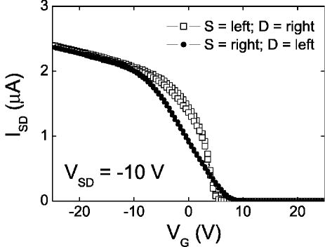
It is commonly believed that the sub-threshold slope is mainly determined by the quality of insulator/semiconductor interface Sze81 . This is definitely the case for Si MOSFETs, where the resistance of source and drain contacts is low and does not depend on the gate voltage. In contrast, the contact resistance in the Schottky-type OFETs is high, it depends non-linearly on - as the result, the sub-threshold slope might reflect the quality of contacts rather than the insulator/semiconductor interface. The effect of the contacts is illustrated in Fig. 19 for a rubrene device fabricated by electrostatic bonding. In this device, interchanging the source and drain contacts results in different sub-threshold characteristics. At higher values of , when the conducting channel is formed, the electrical characteristics are symmetric, i.e. they are not sensitive to the source/drain configuration. Note that in this device the contacts dominate the behavior in the sub-threshold region even though the length of the channel is considerable (1.2 mm; the channel width is approximately 0.2 mm).
III.4 Double-gated rubrene FETs
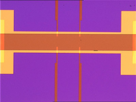
The conventional method for the fabrication of low-resistance contacts in Si MOSFETs is based on ion implantation of dopants beneath the contact area. Unfortunately, a similar technique has not been developed for OFETs yet. In this situation, the contact resistance can be reduced by using the so-called double gate, a trick that has been successfully applied for the study of high-mobility Si MOSFETs at low temperatures Klapwijk98 . Schematic design of such device, fabricated at Rutgers, is shown in Fig. 20.
Two separately biased gate electrodes are deposited on the surface of a rubrene crystal with pre-formed source and drain contacts: the main gate and the complementary gate. These electrodes are isolated from the crystal and each other by a layer of parylene (m thick). The complimentary gate electrode (closest to the surface) consists of two stripes, connected together, that overlap with the source and drain contacts. The resistance of Schottky barriers and the charge density in the channel of this device can be controlled separately by applying different voltages to the complimentary gate, , and to the main gate electrode, .
The trans-conductance characteristics of the double-gated rubrene FET, , are shown in the Fig. 21 for several values of and a fixed V. Large negative voltage greatly reduces the contact resistance, and the regime of low carrier densities becomes easily accessible. However, the price for this is the non-linearity of trans-conductance characteristics at : a portion of the semiconductor surface beneath the complimentary gate electrode is screened from the field of the main gate electrode, and its resistance does not depend on .
III.5 Mobility
The mobility of carriers at the surface of organic crystals can be estimated from the linear portion of the trans-conductance characteristics, where the conductivity of the channel, , varies linearly with the density of mobile field-induced charges, . The ”intrinsic” mobility, not limited by the contact resistance, can be estimated from the 4-probe measurements as Sze81
| (4) |
where is the potential difference between the voltage probes at a distance from each other, is the channel width, and is the specific capacitance between the gate electrode and the conduction channel. For the 2-probe measurements, in Eq. 4 corresponds to the total length of the conduction channel, and to the source-drain voltage . The latter measurements usually provide a lower estimate for , which approaches the intrinsic value with increasing and (see Fig. 14). Eq. 4 is based on the assumption that all charge carriers induced by the transverse electric field above the threshold are mobile, and their density is given by:
| (5) |
This assumption has not been fully justified yet. For comparison, in a different type of FETs with comparable values of , amorphous silicon (-Si:H) FETs, this is not the case: above the threshold, most of the induced charge in these devices goes into the ”tail” (localized) states with only a small fraction going into the conduction band (see, e.g., Shur89 ). The latter model of multiple thermal trapping and release of carriers involving shallow traps is not appropriate for OFETs, where charge transport cannot be described in terms of band transport owing to polaronic effects Silinsh94 ; Wu97 . Some justification of estimate 5 is provided by observations of -independent mobility and the mobility increase with cooling, in a sharp contrast with the behavior of the -Si:H FETs. Note that, contrary to the conventional inorganic FETs, the density of polaronic charge carriers in OFETs cannot be estimated from the Hall-type experiments, at least at high temperatures where hopping processes govern the charge transport (for discussion of the Hall effect in the polaronic hopping regime, see Ref. Friedman78 ).
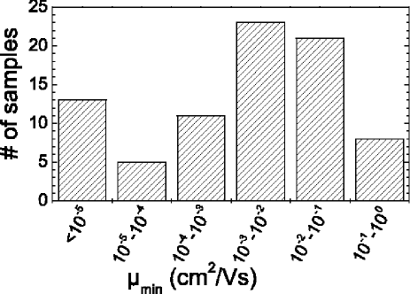
The room temperature mobility of the field-induced carriers varies over a wide range for different organic single crystals. The following values of have been reported: tetracene - 0.4 cm2/Vs DeBoer03 , pentacene - 0.5 cm2/Vs Takeya03 ; Stassen04 , rubrene - 10 cm2/Vs (up to 15 cm2/Vs in recent unpublished measurements Sundar04 ), TCNQ - 1 cm2/Vs Podzorov04 ). For most of these materials, comparable values of have been obtained for FETs fabricated by both techniques of electrostatic bonding and direct fabrication on the crystal surface - another indication of the fact that, in many cases, the measurements with single-crystal OFETs probe the electronic properties of the crystals, at least at room temperature, and are not affected by artifacts due to the device fabrication.
The values for single-crystal devices are comparable or greater than the corresponding values of reported for the best thin-film devices (see, e.g., DeBoer03 ; Gundlach02 ). To our knowledge the only exception is pentacene, for which the highest measured TFT mobility is 3 cm2/Vs. Recently however, a room temperature mobility estimated by in-plane SCLC measurements as high as cm2/Vs has been reported Jurchescu04 . Work on the fabrication of FETs based on these pentacene single-crystals is in progress Stassen04a .
Two inter-related factors play an important role in the mobility improvement in single-crystal OFETs with respect to the organic TFTs. Firstly, the single crystal surfaces are free from the inter-grain boundaries that might limit significantly the mobility in the thin-film devices Horowitz03a . Secondly, the experiments with organic single crystals demonstrated for the first time that the mobility might be strongly anisotropic (see Sec. III.6). Thus, in the experiments with single crystals, there is a possibility to choose the direction of the maximum mobility. In the case of elongated, needle-like crystals (rubrene, pentacene, etc.), the direction of maximum mobility coincides with the direction of the fastest crystal growth with the strongest inter-molecule interactions. At the same time, the mobility of carriers in OTFTs with the grains oriented randomly with respect to the current is an ”angle-averaged” quantity: the grains oriented along the axis of the minimum mobility will have a much higher resistance.
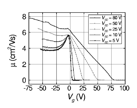
The mobility in the single-crystal OFETs depends much less on the carrier density and the source-drain voltage than that in the organic TFTs. In the latter case, a pronounced increase of with is observed due to the presence of structural defects Dimitrakopoulos02 ; because of the strong dependence in the TFTs, a large V (for a typical m thick SiO2 gate insulator) is often required to realize higher mobilities, comparable to that of -Si:H FETs ( cm2/Vs). The typical dependence of the ”2-probe” on the gate voltage for rubrene OFETs is shown in Fig. 22. The maximum of near the zero and an apparent increase of the mobility with are the artifacts of the 2-probe measurements; these artifacts are caused by a strong -dependence of the resistances of the source and drain contacts Chwang00 . At sufficiently large negative gate voltage ( V), becomes almost -independent (the variations do not exceed ). The dependence of on , measured for the rubrene OFETs in the 2- and 4-probe configurations are compared in the inset to Fig. 14. The 4-probe data reflect the ”intrinsic” charge carrier mobility, which is only weakly dependent on . The 2-probe data converge with the 4-probe data at high owing to a lower contact resistance. Similar independence of the mobility of has been observed for tetracene single crystal FETs DeBoer03 .
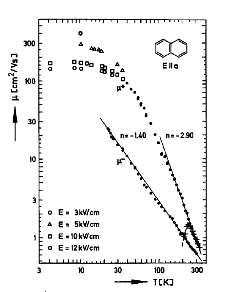
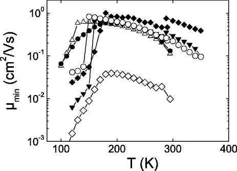
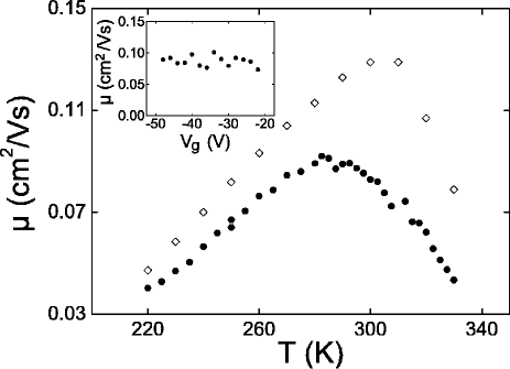
A non-monotonous temperature dependence of has been observed on the devices with highest (for a given material) mobilities: with cooling from room temperature, the mobility initially increases and then drops sharply below K. The temperature dependencies of the mobility for the rubrene (4-probe measurements) and tetracene (2-probe measurements) FETs are shown in Fig. 23 and 24. Similar trend has been observed for the high-mobility pentacene OFETs Nelson98 ; Takeya03 . There is no correlation between the absolute value of (300 K) and its temperature dependence: similar dependencies have been observed for the tetracene OFETs with cm2/Vs and rubrene OFETs with cm2/Vs. The low-temperature drop of can be fitted by an exponential dependence with the activation energy meV. Observation of this drop in the 4-probe measurements indicates that the exponential decrease of the mobility at low temperatures is not an artifact of the 2-probe geometry and rapidly increasing contact resistance.
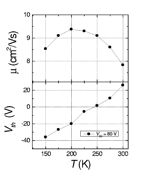
There are some indirect indications that the room-temperature mobility in the devices with a low density of defects (high-purity crystals and high quality of organic surface) approaches its intrinsic value. The increase of with cooling, which is usually considered as a signature of the intrinsic transport, correlates with observation of the mobility anisotropy (see Sec. III.6). The mobility drop, observed with further cooling, resembles the data obtained in the TOF experiments for not-so-pure crystals - this drop is likely caused by trapping of carriers by shallow traps, which can be active above the field-effect threshold due to thermal excitations in the system. An increase of the threshold voltage with cooling, clearly seen in Fig. 23, indicates that the trap concentration is relatively large even in the best crystals that have been used so far for the OFET fabrication. At present, the quantitative description of the polaronic transport, in general, and interaction of polarons with shallow traps in the FET experiments, in particular, is lacking. More systematic four-probe measurements of in different molecular crystals, along with the theoretical efforts on description of polaronic transport in systems with disorder, are needed to understand the origin of the observed temperature dependence of the mobility.
III.6 Mobility anisotropy on the surface of organic crystals.
Because of a low symmetry of organic crystals, one expects a strong anisotropy of their transport properties. Indeed, a strong anisotropy of the polaronic mobility with respect to the crystallographic orientation has been demonstrated by the TOF experiments Karl99 ; Karl85a ; Karl01 . Observation of the mobility anisotropy can be considered as a prerequisite for observation of the intrinsic (not limited by disorder) transport in organic semiconductors. The measurements on thin-film organic transistors never revealed such anisotropy. By eliminating grain boundaries and other types of defects, fabrication of the single-crystal OFETs allow for the first time to address the correlation between the molecular packing and the anisotropy of the charge transport on the surface of organic crystals.
To probe the mobility anisotropy on the a-b surface of the rubrene crystals, the researchers in Ref. Sundar04 exploited an advantage of the PDMS stamp technique, which allows re-establishing the contact between the stamp and some organic crystals without damaging the surface. In this experiment, the crystal was rotated in a step-wise fashion, after each rotation the 2-probe stamp was re-applied, and the mobility was measured in both linear and saturation regime to exclude the effect of contacts. Figure 25b shows the data for two rotations, to demonstrate reproducibility of the results. Black and red symbols correspond to the values extracted from the linear and saturation regimes of the FET characteristics, respectively. The agreement between these values confirms that the contact effects can be neglected. Combination of the orientation-dependent field-effect transport measurements with the Laue x-ray analysis of the crystals shows that the direction of the highest mobility coincides with the b-axis (see Fig. 25a).
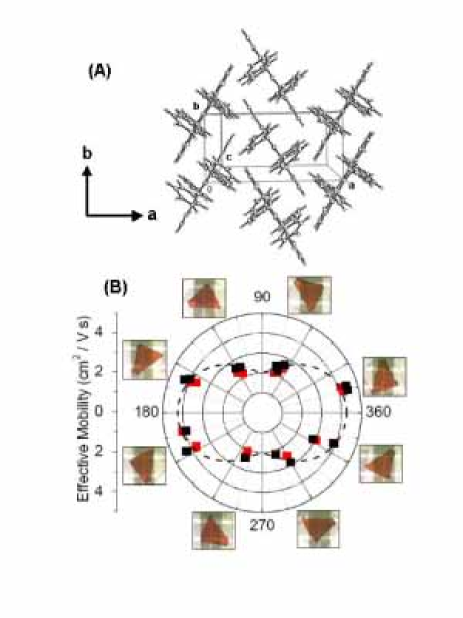
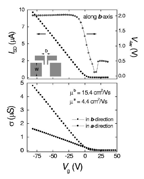
The channel conductivity, , extracted from the 4-probe measurements along the directions of maximum and minimum mobility (the b and a crystallographic axes, respectively) are shown in Fig. 26. The mobility along the b-axis is almost 4 times greater than the mobility along the a axis.
III.7 Preliminary results for the OFETs with high-k dielectrics.
The characteristics of OFETs with high-k gate dielectrics (see Sec. II.3.1) are in many respects similar to those for devices with the SiO2 gate dielectric. The curves measured for a tetracene FET electrostatically bonded onto a Ta2O5 insulating layer are shown in Fig. 27. Although the leakage gate current is normally higher than that for SiO2, it is still significantly smaller than the source-drain current. The maximum charge density that has been reached so far is cm-2.
Despite apparent similarity, there is a significant difference between FETs fabricated on SiO2 and on Ta2O5: the characteristics of high-k OFETs degrade substantially upon successive measurements. Specifically, the source-drain current measured at a fixed source-drain voltage is systematically decreased when subsequent scans of the gate voltage are performed. In general, the higher the applied gate voltage, the stronger the degradation. At the same time, the threshold voltage systematically increases to higher (negative) values.
For the case of Ta2O5, this degradation eventually results in a complete suppression of the field effect. This is shown in Fig. 28 where the source, the drain and the leakage current are plotted as a function of the gate voltage, for a fixed source/drain voltage ( V). Instead of increasing linearly with as in conventional FETs, the source/drain current exhibits a maximum (at V in this device) and then decreases to zero upon further increasing . This degradation is completely irreversible: no measurable source/drain current was detected when was decreased to 0 and swept again to high voltage.
The experiments show that current leaking from the gate is the cause of the FET degradation. This current, typically much smaller than the source-drain current (see Fig. 28), has a different effect: the electrons leaking through the gate insulator, accelerated in a strong electric field due to the voltage applied to the gate electrode, damage the organic crystals. The precise microscopic mechanism responsible for the damage is still unclear, but it is likely that the injection of high-energy electrons introduces surface defects (locally disrupting the crystal due to the accumulation of negative charge) and result in formation of traps (e.g., ”broken” individual moleucles). This would account for the observed decrease in mobility and shift in threshold voltage.
Optimization of the growth of high-k dielectrics in a near future is possible, since it is known how to reduce the leakage current by several orders of magnitude (by sputtering the high-k materials onto a heated substrate Fleming00 ). This is known to bring it to the level observed in SiO2 ( A/cm2 for a SiO2-thickness of 200 nm), at which the irreversible damage introduced in the crystal is minimal. This improvement will allow stable FET operation at a charge density cm-2.
IV Conclusion
The development of single-crystal OFETs offers a great opportunity to understand better the charge transport in organic semiconductors and to establish the physical limits on the performance of organic field-effect transistors. Below we briefly summarize the recent progress in this field, and attempt to formulate the research directions that, from our viewpoint, need to be addressed in the near future.
One of the central issues in the field-effect experiments with organic semiconductors is realization of the intrinsic (not limited by disorder) charge transport on the organic surface. In disorder-free organic semiconductors, several regimes of polaronic transport are expected (see, e.g., Silinsh94 ; Fratini03 ), between the limiting cases of the coherent motion in extended states (band-like polaronic transport) at low temperatures and the incoherent hopping at high temperatures. All these regimes are intrinsic in the aforementioned sense and all of them require better understanding: the incoherent polaronic hopping is pertinent, for instance, to the devices functioning at room temperature, whereas the realization of band-like polaronic transport is the Holy Grail of basic research.
We have witnessed significant progress towards realization of this goal. In this respect, an important characteristic of the first generation of single-crystal OFETs, whose significance should not be underestimated, is the device reproducibility and consistency of experimental observations - e.g., similar mobilities have been observed for the single-crystal OFETs based on the same organic compound but fabricated by different teams using different fabrication techniques. Although it might be taken for granted that this should be the case, such reproducibility has never been achieved in thin-film organic field effect transistors: the organic TFTs are notoriously known for a large spread of parameters, even if they were prepared under nominally identical conditions Dimitrakopoulos02 ; Campbell01 . This irreproducibility is still a problem despite the fact that OTFTs have been the subject of intense research for a much more extended period of time than single crystal OFETs.
The reproducibility of the OFET parameters is a necessary condition for investigation of the intrinsic electronic properties of organic semiconductors; the reproducibility, however, does not guarantee that the electrical behavior of the first-generation single crystal OFETs reflects the intrinsic electronic properties of organic molecular materials. Indeed, all OFETs investigated by different research groups have been fabricated on the basis of crystals grown under similar conditions, and, presumably, with a similar concentration of defects. Thus, the question remains: how close are we to the realization of the intrinsic transport in organic single crystal FETs?
For different temperature ranges, the answer to this central question will be different. There are many indications that at room temperature, the best single-crystal OFETs demonstrate the intrinsic behavior, and the room-temperature mobility of these devices approaches its intrinsic value. For example, observation of the anisotropy of the mobility of field-induced charges in the a-b plane Sundar04 reveals for the first time (in the FET experiments) correlation between the charge transport and the underlying lattice structure. Another important observation is a moderate increase of the mobility with cooling (over a limited range), similar to the case of ”bulk” transport in the TOF experiments. Does this mean that these devices disorder-free? Of course, it does not. Since this characteristic time of the charge release by shallow traps decreases exponentially with the temperature, the shallow traps might be ”invisible” at room temperature. However, with cooling, they start dominating the charge transport in single-crystal OFETs, as all the data obtained so far suggest: the mobility drops exponentially, typically below 100 K. In this respect, the low-temperature dependence observed in the best single-crystal OFETs resemble the results of TOF experiments with not-so-pure ”bulk” crystals. The observed exponential drop of with cooling suggests that the density of shallow traps near the surface of organic crystals in single-crystal OFETs is still relatively large.
Though the low-temperature transport in single-crystal OFETs is, most likely, disorder-dominated, it is worth considering alternative explanations of a qualitative difference between the results of OFET and TOF experiments. It is usually tacitly assumed that the ”surface” transport in OMCs is similar to the ”bulk” transport, which has been comprehensively studied in the 70s and 80s (see, e.g., Pope99 ). However, the transport in organic FETs differs from the ”bulk” charge transport in the TOF experiments at least in two important aspects. Firstly, one cannot exclude a priori the existence of some surface modes that might affect the charge transport at the organic/insulator interface. Secondly, even at a low gate voltage, the density of charge carriers in a two-dimensional conducting channel of OFETs exceeds by far the density of charges in the TOF experiments. The interactions between polaronic excitations and their effect on the charge transport in organic semiconductors is still an open issue Capone03 . Thus, the experiments with single-crystal OFETs pose new problems, which have not been addressed by the theory yet.
Quantitative description of polaronic formation is a challenging many-body problem. Band-type calculations for OMC provide guidance in the search for new high-mobility materials, but do not have predictive power since they ignore polaronic effects Silinsh94 . For better characterization of the polaronic states at the organic surface, it is crucial to go beyond the dc experiments and to measure directly the characteristic energies involved in polaron formation. This information can be provided by the infra-red spectroscopy of the conduction channel in the single-crystal OFETs, a very promising direction of the future research.
Though the current efforts are mostly focused on realization of the intrinsic polaronic transport, equally important is to study interaction of polarons with disorder. From the history of physics of inorganic semiconductors, we know how important is this research for better understanding of charge transport and device characteristics. In organic conductors, small polarons interact strongly with disorder, and this interaction is qualitatively different from the interaction of electron-like excitations with disorder in inorganic semiconductors. This research, which encompasses such important issues as the spectroscopy of the states in the band gap, mechanisms of polaron trapping by shallow and deep traps, polaron scattering by defects in a strongly-anisotropic medium will be critically important for both basic science and applications. One of the aspects of this general problem is the effect of stress on polaronic motion. Indeed, in the field-effect experiments, it is difficult to avoid the build-up of mechanical stress, caused by the difference in the thermal expansion coefficients for the materials that form an OFET. The stress in organic crystals might affect strongly the overlap between electronic orbitals, the density of defects, and, as the result, the temperature dependence of the mobility in the FET experiments. More experiments with different FET structures are needed to clarify this issue.
Realization of the intrinsic transport, especially at low temperatures, requires better purification of starting material and improvement of the crystal growth techniques. There is ample room for improvement in this direction: the first experiments on fabrication of single-crystal OFET did not use a powerful zone-refinement technique, which has been proven to be very useful in the TOF experiments Karl80 ; Karl85 . In fact, many of the molecules used in FET experiments, including rubrene, can be zone refined.
To understand better the intrinsic transport in organic semiconductors and the relation between macroscopic electronic properties and molecular packing, the experiments with OFETs based on a broader class of organic crystals are required. Note that the experiments with any type of organic crystals, regardless of the magnitude of the intrinsic mobility, are important - in fact, only by exploring materials with different crystal structures and, hence, a wide range of , this problem can be adequately addressed. However, realization of the coherent band-like transport and improvement of the room-temperature mobility in OFETs will be helped by the development of new organic materials with a stronger overlap between electronic orbitals of adjacent molecules. In this regard, the materials with a non-planar molecular structure similar to that of rubrene (conjugated chains with non-planar side groups) seem to be very promising (see, e.g., Anthony02 ). Recent experiments with rubrene, which enabled a 10-fold increase of the OFET mobility, illustrates how important is the effect of molecular packing on the charge transport in organic crystals. To realize the enormous potential of organic chemistry in ”tailoring” new organic compounds for organic electronics, combined efforts of chemists and physicists are required.
The use of a broader variety of organic compounds for the OFET fabrication may also offer the possibility to explore new electronic phenomena. An interesting example is provided by the metal-phthalocyanines (MPc’s), a large class of materials with isostructural molecules that differ by only one atom - the metal element. This metal atom determines the electronic properties of the molecules, including the spin S in the molecular ground state Clack72 ; Liao01 . For instance, among the MPc’s containing transition metal elements, MnPc has S Awaga91 , FePc has S Evangelisti02 , CoPc and CuPc have S Liao01 . In FETs based on these materials, therefore, it may be possible to induce and control electrostatically the magnetic properties of organic materials, just by tuning the density of mobile charge carrier that mediate interactions between the local spins. Successful realization of ’magnetic’ OFETs would open the way for organic spintronics.
V Acknowledgments
We are grateful to M. Jochemsen, N. Karl, V. Kiryukhin, T. M. Klapwijk, Ch. Kloc, J. Niemax, J. Pflaum, V. Pudalov, J. Rogers, and A. F. Stassen for useful discussions and help with experiments. The work at Rutgers University was supported in part by the NSF grant DMR-0077825 and the DOD MURI grant DAAD19-99-1-0215. Work at Delft University was supported by the ”Stichting FOM” (Fundamenteel Onderzoek der Materie) and by NWO via the Vernieuwingsimpuls 2000 program.
References
- (1) E. A. Silinsh, and V. Čápek, Organic Molecular Crystals: Interaction, Localization, and Transport Phenomena (AIP Press, Woodbury, 1994)
- (2) M. Pope, and C. E. Swenberg, Electronic Processes in Organic Crystals and Polymers, 2nd ed. (Oxford University Press, New York, London, 1999)
- (3) R. Farchioni, and G. Grosso, Organic electronic Materials (Springer-Verlag, Berlin, 2001)
- (4) N. Karl, In: Crystals, Growth, Properties and Applications, Vol. 4, ed. by H. C. Freyhardt (Springer-Verlag, Berlin 1980) pp. 1-100
- (5) W. Warta, and N. Karl, Phys. Rev. B 32, 1172 (1985)
- (6) N. Karl, K.-H. Kraft, J. Marktanner, M. Münch, F. Schatz, R. Stehle, and H.-M. Uhde, J. Vac. Sci. Technol. A 17, 2318 (1999)
- (7) S. M. Sze, Physics of Semiconductor Devices (Wiley, New York, 1981)
- (8) A. T. Fiory, A. F. Hebard, R. H. Eick, P. M. Mankiewich, R. E. Howard, and M. L. O Malley, Phys. Rev. Lett. 65, 3441 (1990); J. Mannhart, J. Bednorz, K. A. Muller, and D. G. Schlom, Z. Phys. B 83, 307 (1991); J. Mannhart, Supercon. Sci. Technol. 9, 49 (1996); N. Chandrasekhar, O. T. Valls, and A. M. Goldman, Phys. Rev. B 54, 10218 (1996); P. Konsin, and B. Sorkin, Phys. Rev. B 58, 5795 (1998); C. H. Ahn, S. Gariglio, P. Paruch, T. Tybell, L. Antognazza, and J.-M. Triscone, Science 284, 1152 (1999)
- (9) S. Mathews, R. Ramesh, T. Vankatesan, and J. Benedetto, Science 276, 238 (1997); H. Ohno, D. Chiba, F. Matsukura, T. Omiyra, E. Abe, T. Dietl, Y. Ohno, and K. Ohtani, Nature 408, 944 (2000); H. Tanaka, J. Zhang, and T. Kawai, Phys. Rev. Lett. 88, 027204 (2002)
- (10) D. M. Newns, J. A. Misewich, C. C. Tsuei, A. Gupta, B. A. Scott, and A. Schrott, Appl. Phys. Lett. 73, 780 (1998)
- (11) H.-T. Kim, B. G. Chae, D. H. Youn, S. L. Maeng, and K. Y. Kang, cond-mat/0308042
- (12) H. Ohno, D. Chiba, F. Matsukura, T. Omiyra, E. Abe, T. Dietl, Y. Ohno, and K. Ohtani, Nature 408, 944 (2000)
- (13) G. Horowitz, Adv. Mater. 10, 365 (1998)
- (14) H. E. Katz, and Z. Bao, J. Phys. Chem. B 104, 671 (2000)
- (15) Z. Bao, A. Dodabalapur, and A. J. Lovinger, Appl. Phys. Lett. 69, 4108 (1996); H. Sirringhaus, P. J. Brown, R. H. Friend, M. M. Nielsen, K. Bechgaard, B. M. W. Langeveld-Voss, A. J. H. Spiering, R. A. J. Janssen, E. W. Meijer, P. Herwig, D. M. de Leeuw, Nature 401, 685 (1999)
- (16) G. H. Gelinck, T. C. T. Geuns, and D. M. de Leeuw, Appl. Phys. Lett. 77, 1487 (2000)
- (17) C. D. Dimitrakopoulos, and P. R. L. Malenfant, Adv. Mater. 14, 99 (2002)
- (18) G. Horowitz, Adv. Funct. Mater. 13, 53 (2003)
- (19) I. H. Campbell, and D. L. Smith, Solid State Phys. 55,1 (2001)
- (20) M.C.J.M. Vissenberg, and M. Matters, Phys. Rev. B 57, 12964 (1998)
- (21) S. F. Nelson, Y. -Y. Lin, D. J. Gundlach, and T. N. Jackson, Appl. Phys. Lett. 72, 1854 (1998)
- (22) V. Podzorov, V. M. Pudalov, and M. E. Gershenson, Appl. Phys. Lett. 82, 1739 (2003)
- (23) V. Podzorov, S. E. Sysoev, E. Loginova, V. M. Pudalov, and M. E. Gershenson, Appl. Phys. Lett. 83, 3504 (2003)
- (24) R. W. I. de Boer, T. M. Klapwijk, and A. F. Morpurgo, Appl. Phys. Lett. 83, 4345 (2003)
- (25) J. Takeya, C. Goldmann, S. Haas, K. P. Pernstich, B. Ketterer, and B. Batlogg, J. Appl. Phys. 94, 5800 (2003)
- (26) V. V. Butko, X. Chi, D. V. Lang, and A. P. Ramirez, Appl. Phys. Lett. 83, 4773 (2003)
- (27) V. V. Butko, X. Chi, and A. P. Ramirez, Solid State Commun 128, 431 (2003)
- (28) G. Horowitz, F. Garnier, A. Yassar, R. Hajlaoui, and F. Kouki, Adv. Mater. 8, 52 (1996)
- (29) M. Ichikawa, H. Yanagi, Y. Shimizu, S. Hotta, N. Suganuma, T. Koyama, and Y. Taniguchi, Adv. Mater. 14, 1272 (2002)
- (30) A. F. Hebard, M. J. Rosseinsky, R. C. Haddon, D. W. Murphy, S. H. Glarum, T. T. M. Palstra, A. P. Ramirez, and A. R. Kortan, Nature 350, 600 (1991); O. Gunnarsson, E. Koch, and R. M. Martin, Phys. Rev. B 54, 11026 (1996)
- (31) Ch. Kloc, P. G. Simpkins, T. Siegrist, and R. A. Laudise, J. Cryst. Growth 182, 416 (1997)
- (32) R. A. Laudise, Ch. Kloc, P. G. Simpkins, and T. Siegrist, J. Crystal Growth 187, 449 (1998)
- (33) M. Mas-Torrent, M. Durkut, P. Hadley, X. Ribas, and C. Rovira, J. Am. Chem. Soc. 126, 984 (2004)
- (34) R. Dabestani, M. Nelson, and M. E. Sigman 64, 80 (1996)
- (35) R. A. Laudise, The Growth of Single Crystals (Englewood Cliffs, N. J., Prentice-Hall, 1970)
- (36) R. W. I. de Boer, M. Jochemsen, T. M. Klapwijk, A. F. Morpurgo, J. Niemax, A. K. Tripathi, and J. Pflaum, J. Appl. Phys. 95, 1196 (2004)
- (37) G. Horowitz, B. Bachet, A. Yassar, P. Lang, F. Demanze, J. -L. Fave, and F. Garnier, Chem. Mater. 7, 1337 (1995); T. Siegrist, R. M. Fleming, R. C. Haddon, R. A. Laudise, A. J. Lovinger, H. E. Katz, P. M. Bridenbaugh, and D. D. Davis, J. Mater. Res. 10, 2170 (1995)
- (38) U. Sondermann, A. Kutoglu, and H. Bässler, J. Phys. Chem. 89, 1735 (1985)
- (39) J. Vrijmoeth, R. W. Stok, R. Veldman, W. A. Schoonveld, and T. M. Klapwijk, J. Appl. Phys. 83,3816 (1998)
- (40) D. C. Hoesterey, and G. M. Letson, J. Phys. Chem. Solids 24, 1609 (1963)
- (41) J. Pflaum, private communication
- (42) N. Karl, Organic Semiconductors, In: Landolt-Boernstein (New Series), Group III, Vol. 17 Semiconductors, ed. by O. Madelung, M. Schulz, H. Weiss, (Springer-Verlag Berlin, Heidelberg, New York, Tokyo 1985) Subvolume 17i, pp. 106-218. Updated edition: Vol. 41E (2000)
- (43) N. Karl, J. Martanner, Mol. Cryst. Liq. Cryst. 355, 149 (2001)
- (44) M. A. Lampert, and P. Mark, Current Injection in Solids(Academic Press Inc., New York, 1970)
- (45) K. C. Kao, and W. Hwang, Electrical Transport in Solids (Pergamon Press, Oxford, 1981)
- (46) J. Zaumseil, T. Someya, Z. N. Bao, Y. L. Loo, R. Cirelli, and J. A. Rogers, Appl. Phys. Lett. 82, 793 (2003)
- (47) O. Jurchescu, and T. T. M. Palstra, private communication
- (48) V. C. Sundar, J. Zaumseil, V. Podzorov, E. Menard, R. L. Willett, T. Someya, M. E.Gershenson, and J. A. Rogers, submitted to Science
- (49) R. B. van Dover, L. D. Schneemeyer, and R. M. Fleming, Nature 392, 162 (1998)
- (50) W. Ren, S. Trolier-McKinstry, C. A. Randall, and T. R. Shrout, J. Appl. Phys. 89, 767 (2001)
- (51) R. M. Fleming, D. V. Lang, C. D. W. Jones, M. L. Steigerwald, D. W. Murphy, G. B. Alers, Y. H. Wong, R. B. van Dover, J. R. Kwo, and A. M. Sergent, J. Appl. Phys. 88, 850 (2000)
- (52) C. Shen, and A. Kahn, J. Appl. Phys. 90, 4549 (2001)
- (53) J. Liu, T. Guo, Y. Shi, and Y. Yang, J. Appl. Phys. 89, 3668 (2001)
- (54) D. B. A. Rep, A. F. Morpurgo, and T. M. Klapwijk, Organic Electronics 4, 201 (2003)
- (55) W. Gao, and A. Kahn, Appl. Phys. Lett. 82, 4815 (2003)
- (56) R. W. I. de Boer, A. F. Stassen, T. M. Klapwijk, and A. F. Morpurgo, unpublished results
- (57) H. Klauk, M. Halik, U. Zschieschang, G. Schmid, W. Radlik, and W. Weber, J. Appl. Phys. 92, 5259 (2002)
- (58) E. J. Meijer, D. M. de Leeuw, S. Setayesh, E. van Veenendaal, B. -H. Huisman, P. W. M. Blom, J. C. Hummelen, U. Scherf, and T. M. Klapwijk, Nature Materials 2, 678 (2003)
- (59) The total number of the ”bulk” charge traps per the unit area of the conducting channel can be estimated as , where cm-3 is the bulk concentration of traps, and is the effective channel thickness ( nm). The corresponding threshold voltage, associated with the bulk traps in the studied devices, is therefore very small ( V).
- (60) C. D. Dimitrakopoulos, S. Purushothaman, J. Kymissis, A. Callegari, and J. M. Shaw, Science 283, 822 (1999)
- (61) Y. -Y. Lin, D. J. Gundlach, S. F. Nelson, and T. N. Jackson, IEEE Trans. Electron Devices 44, 1325 (1997); H. Klauk, D. J. Gundlach, J. A. Nichols, and T. N. Jackson, IEEE Trans. Electron Devices 46, 1258 (1999)
- (62) C. D. Dimitrakopoulos, I. Kymissis, S. Purushothaman, D. A. Neumayer, P. R. Duncombe, and R. B. Laibowitz, Adv. Mater. 11, 1372 (1999)
- (63) J. Kanicki, F. R. Libsch, J. Griffith, and R. Polastre, J. Appl. Phys. 69, 2339 (1991)
- (64) R. Heemskerk, and T. M. Klapwijk, Phys. Rev. B 58, R1754 (1998)
- (65) M. Shur, M. Hack, and J. G. Shaw, J. Appl. Phys. 66, 3371 (1989).
- (66) M. W. Wu, and E. M. Conwell, Chem. Phys. Lett. 266, 363 (1997).
- (67) L. Friedman, Phil. Mag. 38, 467 (1978)
- (68) A. F. Stassen, R. W. I. de Boer, T. M. Klapwijk, and A. F. Morpurgo, work in progress
- (69) V. Podzorov, and M. E. Gershenson, work in progress
- (70) D.J. Gundlach, J.A. Nichols, L. Zhou, and T.N. Jackson, Appl. Phys. Lett. 80, 2925 (2002)
- (71) O. D. Jurchescu, J. Baas, and T. T. M. Palstra, to be published in Apl. Phys. Lett.
- (72) O. D. Jurchescu, A. F. Stassen et al., work in progress
- (73) G. Horowitz, Synth. Met. 138, 101 (2003)
- (74) A. B. Chwang, and C. D. Frisbie, J. Phys. Chem. B 104, 12202 (2000); P. V. Necliudov, M. S. Shur, D. J. Gundlach, and T. N. Jackson, Solid State Electron. 47, 259 (2003); J. Zaumseil, K. W. Baldwin, and J. A. Rogers, J. Appl. Phys. 93, 6117 (2003)
- (75) S. Fratini, and S. Ciuchi, Phys. Rev. Lett. 91, 256403 (2003)
- (76) M. Capone, and S. Ciuchi, Phys. Rev. Lett. 91, 186405 (2003)
- (77) J. E. Anthony, D. L. Eaton, and S. R. Parkin, Org. Lett. 4, 15 (2002)
- (78) D. W. Clack, and J.R. Yandle, Inorg. Chem. 11, 1738 (1972)
- (79) M.S. Liao, and S. Scheiner, J. Chem Phys. 114, 9780 (2001)
- (80) K. Awaga and Y. Maruyama, Phys. Rev. B 44, 2589 (1991)
- (81) M. Evangelisti, J. Bartolome, L. J. de Jongh, and G. Filoti, Phys. Rev. B 66, 144410 (2002)