Influence of manganese contamination on high-mobility GaAs/AlGaAs heterostructures
Abstract
Photoluminescence and magnetotransport measurements have been performed to assess the quality of modulation doped GaAs/AlGaAs heterostructures. The temporal evolution of the low-temperature electron mobility of samples prepared in a molecular beam epitaxy chamber containing manganese as a source material was studied. Mn contamination was identified to be responsible for the reduction of the electron mobility to 1 106 cm2/Vs and the appearance of a distinct photoluminescence band. In contrast, structures in which this signal is absent reach mobility values of 5.4 106 cm2/Vs. This directly proves that the epitaxy of high-mobility electron systems and structures containing GaMnAs layers, in principle, can be combined in one growth chamber.
Modulation doped GaAs/AlGaAs heterostructures have been the subject of interest for several years mainly for the excellent transport properties of the two dimensional electron gas (2DEG) forming at the heterojunction interface. Molecular beam epitaxy (MBE) is the predestined technique for the growth of such structures, because it allows abrupt doping concentrations and sharp interfaces 1,2. The separation of the doping layer from the electron channel drastically increases low-temperature electron mobilities. In the highest-mobility structures residual impurities in the GaAs layer hosting the 2DEG were identified as the major limiting scattering mechanism 3,4. Thus the essential premise for the growth of high-quality samples is maximum purity of the MBE system and the source materials.
Another recent application area of MBE-grown structures is the rapidly developing field of spintronics, i. e. the coupling of traditional properties of compound semiconductor materials with the spin properties of ferromagnetic materials 5. GaMnAs has emerged as a prime candidate for the investigation of these so-called diluted semiconductors 6. However, the combination of high-mobility electron systems with these ferromagnetic materials, which could be employed as a spin-polarizing injector into a 2DEG, has not been attempted so far. This is due to the general believe that Mn-impurities, once present in the MBE ultra-high vacuum chamber, would drastically limit the achievable electron mobilities for this growth system.
In this letter we report the influence of Mn, which can be unintentionally incorporated during growth, on the quality of modulation doped GaAs/AlGaAs samples. Photoluminescence was used to identify residues of manganese in these structures, and the electronic properties, in particular charge carrier densities and mobilities, were determined by magnetotransport measurements. We find low-temperature mobilities in excess of 5 106 cm2/Vs in samples which were prepared directly after a sample containing GaMnAs had been fabricated. Even in a sample grown on a heavily Mn-contaminated substrate block this value is only decreased to about 1 106 cm2/Vs.
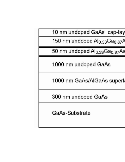
The standard modulation-doped single interface (MDSI) sample structure, schematically depicted in Figure 1, was grown by MBE on a (001)-oriented GaAs substrate typically at 635∘ C. The MBE system, which was manufactured by Veeco Instruments Inc., is based on a Varian Gen II design and equipped with high-capacity closed-cycle refrigerator cryogenic pumps. As a buffer layer we grew 300 nm GaAs followed by a 1000 nm thick GaAs/AlGaAs superlattice. This concept has been shown to significantly improve the quality of structures placed on it, as p-type impurities migrating from the substrate are trapped in the superlattice 7. Onto this buffer an undoped 1000 nm thick GaAs layer and a 50 nm thick Al0.33Ga0.67As spacer layer were grown. The 2DEG is formed at the GaAs/AlGaAs interface and the electrons are supplied by a Si--doped AlGaAs donor layer. All investigated samples were grown with the same set of process parameters.
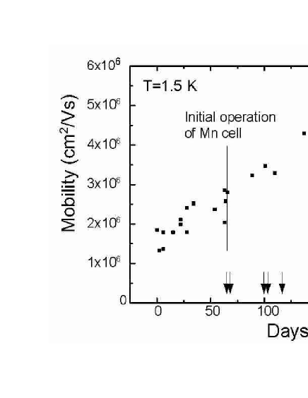
The electronic properties of our samples were investigated by the Van der Pauw method at 1.5 K. In order to ionize deep DX centers in the AlGaAs, each sample was illuminated using a red light emitting diode before the measurement. Figure 2 illustrates the temporal evolution of the mobilities of these standard MDSI structures, which were grown in an MBE system equipped with a Mn effusion cell. The vertical line indicates the initial startup of the manganese cell and the arrows at the bottom of the graph mark dates when GaMnAs or GaAlMnAs samples with typical Mn concentrations of 3 to 5 % were prepared. We find a steady increase of mobility at consistent electron densities of about 3 1011 cm-2. A maximum value in mobility of 5.4 106 cm2/Vs was reached after 210 days of operation (sample A). In order to study the influence of manganese one sample, denoted as sample B, was intentionally grown on a heavily Mn-contaminated substrate holder. This holder was exclusively used for GaMnAs growth so far. This led to a drop in electron mobility down to 1.0 106 cm2/Vs. Sample C was grown some days later on a clean mount and exhibits again a mobility of more than 5 106 cm2/Vs. This result makes clear that the decrease in mobility of sample B is definitely due to the incorporation of Mn. In addition, no memory effect is observed. Obviously the initial startup of the Mn cell and its regular use did not affect the quality of the samples.
In order to prove the incorporation of manganese, we performed photoluminescence measurements of sample A and B. Photoluminescence is a highly sensitive tool for the detection of residual impurities in semiconductor crystals. In addition to the bright excitonic luminescence, defect related recombination bands can be observed. After excitation of the sample, donor bound electrons can recombine with acceptor bound holes. This donor acceptor pair transitions yield a characteristic luminescence band. The energetic position of its maximum in intensity strongly depends on the ionization energies of the participating defects and thus on the type of the impurities. The intensity gives qualitative information about the concentration of the defects. In GaAs, manganese on a gallium-site forms a deep acceptor level at about 0.13 eV above the top of the GaAs valence band. It is well-known that the Mn-related low-temperature PL-signal in GaAs appears at about 1.41 eV in the spectrum. Its origin is the donor acceptor pair transition 8,9. This gives us a sensitive tool to proof the presence of Mn in the GaAs layer of MDSI samples even at very low concentrations.
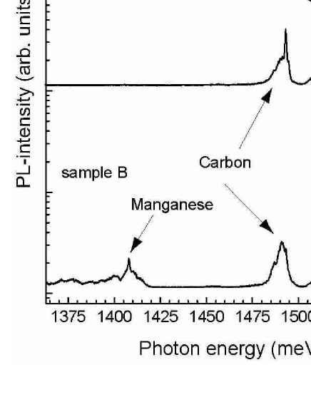
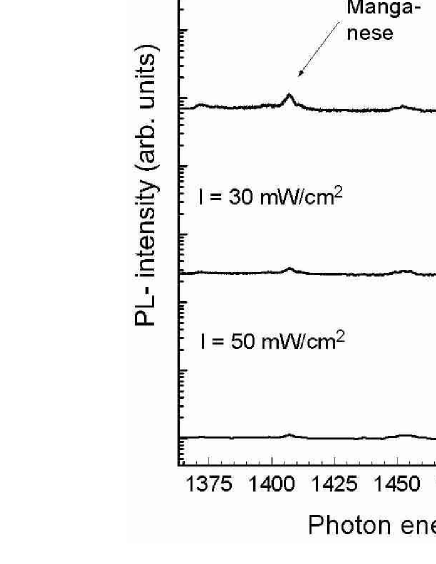
We used a He-Ne-Laser with a maximum output power of 12 mW at = 632.8 nm as an excitation source. The excitation intensity was varied by means of neutral density filters. The laser beam is focused on the sample (spot size d 300 m), which is placed in a helium bath cryostat and cooled down to 1.6 K. For the detection of the PL emission we used a combination of a Jobin-Yvon 0.64m monochromator and a nitrogen cooled CCD camera. All information gained by PL is strictly limited to the upper region of the 1000 nm thick GaAs layer for two reasons. First, Al0.33Ga0.67As is not excited by photons with an energy of 1.96 eV ( 632.8 nm) because its band gap energy is about 2 eV. Second, the penetration depth of the 632.8 nm He-Ne laser wavelength in GaAs is about 230 nm, which means that all of the light is absorbed by GaAs and neither the buffer layer nor the substrate are excited 10. Figure 3 shows the PL spectra of sample A and sample B at excitation densities of about 0.5 mW/cm2. Both are dominated by the excitonic recombination lines of bulk GaAs at about 1.51 eV. Further investigations of the excitonic luminescence revealed narrow lines with full width at half maxima (FWHM) smaller than 0.25 meV, which is beyond the spectral resolution of our detection system. This result reveals the high crystal quality and purity of our samples. Both samples show another emission band at about 1.49 eV corresponding to the free-to-bound transition involving the Carbon acceptor. Carbon as an unintentional impurity is well-known but its source is still unclear. Reaction of carbon monoxide or dioxide with either surface arsenic or gallium suboxide (Ga2O), and a free carbon atom is most probable 11. In contrast to sample A, sample B exhibits an additional PL band at about 1.41 eV. Due to the fact that sample B was grown on the Mn-contaminated substrate holder and its energetic position we assign this signal to the Mn impurity. Obviously, desorption and diffusion processes of Mn, which was deposited on the substrate holder earlier, result in an incorporation of Mn in sample B. This Mn-related luminescence band tends to saturate in intensity by increasing excitation density (see Figure 4). The reason for this effect is the finite number of impurities in the material. When all acceptors and donors are neutralized by the charge carriers, this saturation regime is reached. In sample A, which was grown on a clean substrate holder, no Mn-related PL signal could be observed, even at long integration times and high excitation densities.
In summary, PL measurements of modulation doped GaAs/AlGaAs
samples which were grown in a Mn-contaminated MBE chamber have
been performed. We were able to detect a Mn-related luminescence
band in the spectrum of samples grown on a Mn-contaminated
substrate holder. Samples which were mounted on a clean substrate
holder for growth did not exhibit any Mn-related peak in the
photoluminescence signal. Therefore we conclude that these samples
are, to a high degree, free of undesired manganese impurities.
Magnetotransport measurements showed that Mn incorporation even at
rather low concentrations reduces the low-temperature electron
mobility. Nevertheless, we are able to grow high-quality MDSI
structures with mobilities in excess of 5 106
cm2/Vs in an MBE-system, which is also used for the growth of
GaMnAs samples. Most important, no memory effect was observed over
the time of
operation for GaMnAs growth of roughly half a year.
References:
1R. Dingle, H. L. Stormer, A.
C. Gossard, and W. Wiegmann,
Appl. Phys. Lett. 33, 665 (1978).
2H. L. Stormer, R. Dingle, A. C. Gossard, W. Wiegmann, and M.
D. Sturge, Solid State Commun. 29, 705 (1979).
3V. Umansky, R. d. Piciotto, and M. Heiblum, Appl. Phys.
Lett. 71, 683 (1997).
4L. Pfeiffer, K. W. West, H. L. Stormer, and K. W. Baldwin,
Appl. Phys. Lett. 55, 1888 (1989).
5H. Ohno, Science 281, 951 (1998).
6F. Matsukura, H. Ohno, A. Shen, and Y. Sugawara, Phys. Rev.
B 57 R2037 (1998) .
7T. Saku, Y. Hirayama, and Y. Horikoshi, Jpn. J. Appl. Phys. 30, 902 (1991).
8M. Ilegems, R. Dingle, and L. W. Rupp Jr., J. Appl. Phys.
46, 3059 (1975).
9W. Schairer, and M. Schmidt, Phys. Rev. B 10,
2501 (1974).
10D. E. Aspnes, and A. A. Studna, Phys. Rev. B
27, 985 (1983).
11M. A. Herman, and H. Sitter, Molecular Beam Epitaxy
(Springer, Berlin, 1996).