Controllable Flux Coupling for the Integration of Flux Qubits
Abstract
We show a novel method for controlling the coupling of flux-based qubits by means of a superconducting transformer with variable flux transfer function. The device is realized by inserting a small hysteretic dc SQUID with unshunted junctions, working as a Josephson junction with flux-controlled critical current, in parallel to a superconducting transformer; by varying the magnetic flux coupled to the dc-SQUID, the transfer function for the flux coupled to the transformer can be varied. Measurements carried out on a prototype at K show a reduction factor of about between the “on” and the “off” states. We discuss the system characteristics and the experimental results.
pacs:
85.25.Cp, 03.67.LxRecently, different types of qubits, all based on Josephson junctions, have been experimentally demonstrated. Flux Friedman et al. (2000); I.Chiorescu et al. (2003), phase Martinis et al. (2002); Yu et al. (2002) and phase-charge Vion et al. (2002) qubits have been operated as single devices, while charge state qubits have also been used in an entangled couple, showing quantum-coherent behavior Pashkin et al. (2003) and operation as a conditional gate Yamamoto et al. (2003). In the implementation of a system of entangled qubits, one of the challenges is the realization of a connection between different qubits that fulfills the various constraints imposed by the correct qubit operation. The connection should be non dissipative, otherwise the fluctuations related to its dissipation will destroy the coherent state of the connected qubits; this forbids the use of resistive elements or elements that are dissipative even for a short period of time. It should allow a fast switching, namely its switching time should be much faster than the time related to the clock period. It should be simple and reliable, to be integrable with a large numbers of qubits, and the related implementation should be a well-established technology with a very high degree of reliability. Besides, the coupling strength of the connection should be varied from outside, allowing to turn the coupling on and off whenever needed; it must be noted that a scheme with untunable couplings has been proposed Zhou et al. (2002) but not yet implemented in practical realizations.
In order to couple flux qubits, it comes natural to use superconducting transformers. Two schemes for achieving coupling control have been presented recently. In the INSQUID Clarke et al. (2002), which was originally ideated for readout, the flux qubit is placed inside the dc-SQUID of a double-SQUID. The tunable transformer of ref. Filippov et al. (2003), instead, is conceived for gradiometric flux qubits like that of ref. Friedman et al. (2000) and is based on the balancing of a gradiometric transformer by means of two small dc-SQUIDs inserted in the transformer branches.
In this letter we propose a Controllable Flux Coupling (CFC) system, suitable for the connection of one or more flux qubits. The CFC basic idea is to use a superconducting flux transformer, modified with the insertion of a small hysteretic dc SQUID that behaves as a Josephson junction with tunable critical current. By modulating the SQUID critical current by means of an external magnetic field, it is possible to control the flux transfer function through the transformer and therefore the coupling. Compared to other proposed schemes, the CFC has the advantage of being easily coupled to a flux qubit through inductively coupled coils, without requiring a particular geometry for the qubit to be read out.

Our variable transformer (Fig. 1) consists of two arms of inductance , in parallel with a dc-SQUID that performs the control of the magnetic flux transfer. The inner dc-SQUID is a loop of inductance , interrupted by two Josephson junctions of critical current and capacitance ; its dynamics is described by the differences of the superconducting phase across the Josephson junctions, which are linked by the fluxoid equation to the magnetic fluxes and in the left and in the right loops.
Input flux is coupled to the left side through an inductively coupled coil, with flux transforming ratio ; the flux appearing in the left arm is called . The flux response of the variable transformer is read out by a SQUID magnetometer, magnetically coupled to the right side of the transformer with transforming ratio ; the measured quantity is then the flux . A control magnetic flux linked to the inner dc-SQUID modifies the device behavior. Here and in the following, the subscript refers to externally applied signals, while refers to the control loop.
We introduce new coordinates given by linear combinations of the fluxes, and , where is the flux quantum; the corresponding reduced driving fluxes are and . With these coordinates, the 2D potential describing the system dynamics can be written as follows:
| (1) |
where is an effective inductance, is the corresponding reduced inductance, with twice the critical current because of the two junctions in the dc-SQUID, and . Eq.1 has the same form of the potential for a double SQUID Han et al. (1989), with parameters that take into account the gradiometric structure of the device. In the limit for an inner dc-SQUID with a vanishingly small inductance like in our case, i.e. , the degree of freedom related to is frozen and restrained to an equilibrium value , so that the potential becomes a 1D curve in the remaining coordinate :
| (2) |
where and . This is equivalent to the potential of an ordinary rf-SQUID, but here the critical current can be modulated by the external flux linked to the loop of the inner dc-SQUID and the role of reduced inductance is played by the quantity that is not restrained to assume only positive values. By deriving eq. 2 with respect to and setting the derivative to zero, we find the relationship linking and the excitation to find the extremal points:
| (3) |
For the relation is single-valued and the potential presents just one minimum, while for the relation is multi-valued, with more minima separated by potential barriers.
An input signal centered around , with amplitude smaller than a flux quantum, causes a monotonic and single-valued flux response , whose amplitude depends on the control parameter . In a sufficiently small region this response is linear and hence the system behaves as a linear controllable transformer. In this regime the overall transfer parameter , namely which part of the input magnetic flux is transmitted to the output, is given by the slope of the flux characteristics at the flex point . By returning to the quantities (flux coupled to the left arm of the transformer), (transformer response flux) and (flux coupled to the inner dc-SQUID), one can write:
| (4) |
This modulation of the overall transfer parameter , achieved acting on the flux , is the feature that we exploit to obtain a tunable transformer: while keeping the flux working point around zero, the potential is changed in such a way to change the shape of the characteristics and operate between two points with very different responsivity (the “on” and the “off” states). During operation, the system is kept in the same potential well, avoiding sudden dissipative jumps of the system to other minima; besides, the potential change must be fast but still adiabatic. This last requirement represents the main limit on the operating speed of the CFC system; for our test device one can extimate this limit from the plasma frequency , obtaining a value suitable for typical superconducting quantum gates operations.
In order to test the features of the variable transformer, we built an integrated device composed of transformer, excitation coil and non-hysteretic readout dc-SQUID, using trilayer Nb/AlOx/Nb technology. The inner dc-SQUID Cosmelli et al. (2001) is made by two loops in a gradiometric configuration, with an area of , partially covered by the overlaying Nb layer; the total inductance has been evaluated in previous measurements to be about . The junctions have nominally side and a critical current , measured in a similar, isolated device; the corresponding reduced inductance , then, is much less than unity. The inner dc-SQUID is connected in parallel to two Nb coils of inductance , each consisting of two turns wound around a square of side (computed value ). The transformer arms are magnetically coupled respectively to the excitation coil and to the input coil of the readout dc-SQUID, both made of two turns, nested into the rf-SQUID loops and tightly coupled by means of a ground plane; the measured transfer ratio to the readout SQUID is . For this variable transformer, the maximum value of the reduced inductance is .
In the experiment, carried out at , we measured the flux response to a sweeping external flux for different values of the flux applied to the inner dc-SQUID. The experimental curves are shown in Fig. 2a; for clarity, curves with hysteretic behavior, which have been observed in the device, are not displayed. The curves are described by Eq. 3, except for a small shift, both in the horizontal and vertical directions, caused by the unavoidable spurious coupling of the control flux to the transformer input coil and to the readout SQUID. From the measured shifts we estimated the values of the mutual inductance between the control flux coil and the transformer input (), and that between the control flux coil and the readout SQUID (). Fig. 2b shows the experimental curves after correction for the spurious coupling. It was verified experimentally that the input flux produces a negligible spurious effect both on the readout SQUID and on the inner dc-SQUID.
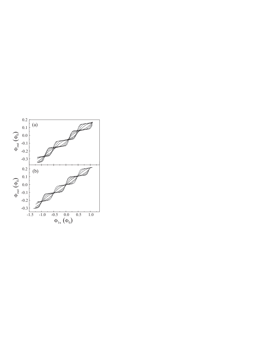
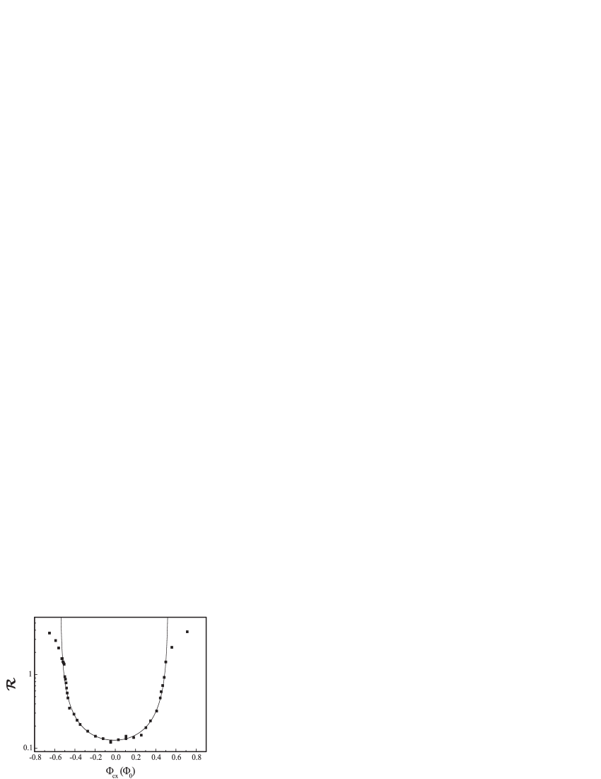
Fig. 3 shows the measured slopes of the acquired characteristics at the working point, namely at the crossing closest to in Fig. 2a, as a function of the control flux. The fit (continuous line) is made using Eq. 4, with spurious coupling taken into account, and allows an independent estimate of that is consistent with the project value. While the agreement is very good in the bottom part of the curve, in the upper part the experimental points are lower than expected. This effect is due to the rounding of the flux characteristics because of thermal fluctuations: the slope in the steepest points is reduced. At lower temperature this smearing effect is expected to decrease with the square root of the temperature, until the classical-quantum crossover temperature is reached (hundreds of for our devices) and quantum tunnelling becomes the dominant fluctuation term. The ratio between minimum and maximum slope (about for the data of Fig. 3) is a figure of merit for the performance of the variable transformer.
Let’s now discuss how the variable transformer works. The “off” state, where the transfer ratio is minimum, is easily identified with the state where the effective reduced inductance is maximum, that is ; to get a small flux transfer, then, the device must be highly hysteretic (large ). In this condition the slope of the flux characteristic is almost horizontal and a large amount of input flux can be fed while keeping the device in the same flux state; this curve is not shown in Fig. 2. By increasing the control flux to , one gets , and the input flux is totally transmitted to the output; however this is not the steepest possible slope, since by further increasing one gets tending to and a diverging . Excluding the non-physical point , we can then increase the transfer ratio beyond unity. Two considerations must be done at this point. First, while the “off” state can be obtained with a hysteretic characteristic (provided that there are no transitions between different flux states), the “on” state must be obtained with non-hysteretic characteristics and this restrains the range of usable values to . Second, the flux response is not necessarily linear with the input flux; the dynamical range where linearity is ensured is depending on the parameter : the steepest is the slope of the flux characteristic, the smaller is the allowed flux range. With larger flux signals, the response has a saturated amplitude and harmonics are produced. However, in certain cases this may not be a limitation: in qubit operation, in fact, generally one has just to distinguish between the two different flux states, the required response being just an identification of the qubit state. In this situation, operating in the non linear range does not affect the efficiency of the measurement and extends the usable range of the input signals. As a matter of fact, choosing the working points for “off” and “on” states is best achieved experimentally, according to the specific requirements of the experiment and to the signal characteristics that must be preserved.
To test the performance of the transformer, we sent a sinusoidal signal to the left side of the transformer and measured the output from the readout dc-SQUID while modulating the inner dc-SQUID with a square wave between the points of maximum and minimum transfer ratio, chosen experimentally.

The resulting modulation is shown in Fig. 4.The measured efficiency, the maximum ratio between the “on” and the “off” transmission, is about , in agreement with the data of Fig. 4. For this situation, the measured range in which the response is linear corresponds a peak-to-peak input flux of . If the linear range is exceeded, the efficiency in the flux modulation decreases but operation is still possible. As an example, for an input flux of peak-to-peak the measured ratio between the “on” and the “off” transmission is about .
CFC systems can be integrated together with the SQUID flux qubits, since they are based on the same technology, and can be used to control the couplings between them. They can also be also used to realize a bus for the controlled coupling of more qubits, for example by using the scheme shown in Fig. 5; in this example a pair of qubits can be coupled by switching “on” the relative “switches”, and by maintaining all the others in the “off” state (this scheme is similar to that proposed in Chiarello (2000)). Since the CFC remains always in the superconducting state without jumps to a dissipative state, the only contribution to the overall decoherence is due to the device intrinsic dissipation and to the enviromental noise pick-up. This means that the total contribution to decoherence should be of the same order of the qubit contribution, since they are very similar for technology, dimensions, components and structure.

In conclusion, we have realized and tested a microfabricated SQUID based controllable flux coupling, useful in any application in which it is necessary to modify the magnetic coupling between different devices, and in particular suitable for quantum computing applications with flux qubits.
This work has been supported by INFN under the project SQC.
References
- Friedman et al. (2000) J. R. Friedman, V. Patel, W. Chen, S. K. Tolpygo, and J. E. Lukens, Nature 406, 43 (2000).
- I.Chiorescu et al. (2003) I.Chiorescu, Y.Nakamura, C. J. P. M. Harmans, and J.E.Mooij, Science 299, 1869 (2003).
- Martinis et al. (2002) J. M. Martinis, S. Nam, and J. Aumentado, Phys. Rev. Lett. 89, 518 (2002).
- Yu et al. (2002) Y. Yu, S. Han, X. Chu, S. Chu, and Z. Wang, Science 296, 889 (2002).
- Vion et al. (2002) D. Vion, A. Aassime, A. Cottet, P. Joyez, H. Pothier, C. Urbina, D. Esteve, and M. H. Devoret, Science 296, 886 (2002).
- Pashkin et al. (2003) Y. A. Pashkin, T. Yamamoto, O. Astafiev, Y. Nakamura, D. V. Averin, and J. S. Tsai, Nature 423, 823 (2003).
- Yamamoto et al. (2003) T. Yamamoto, Y. A. Pashkin, O. Astafiev, Y. Nakamura, and J. S. Tsai, Nature 425, 941 (2003).
- Zhou et al. (2002) X. Zhou, Z. Zhou, G. Guo, and M. J. Feldman, Phys. Rev. Lett. 89, 197903 (2002).
- Clarke et al. (2002) J. Clarke, T. L. Robertson, B. L. T. Plourde, A. Garcia-Martinez, P. A. Reichardt, D. J. van Harlingen, B. Cheasca, R. Kleiner, Y. Makhlin, G. Schoen, et al., Physica Scripta T102, 173 (2002).
- Filippov et al. (2003) T. V. Filippov, S. Tolpygo, J. Mannik, and J. E. Lukens, IEEE Trans. Appl. Superc. 13, 1005 (2003).
- Han et al. (1989) S. Han, J. Lapointe, and J. E. Lukens, Phys. Rev. Lett. 63, 1712 (1989).
- Cosmelli et al. (2001) C. Cosmelli, M. Castellano, P. Carelli, F. Chiarello, R. Leoni, and G. Torrioli, IEEE Trans. Appl. Superc. 11, 990 (2001).
- Chiarello (2000) F. Chiarello, Physics Letters A 277, 189 (2000).