Quantum Dot coupled to a normal and a superconducting lead
Abstract
We report on electrical transport measurements in a carbon nanotube quantum dot coupled to a normal and a superconducting lead. Depending on the ratio of Kondo temperature and superconducting gap the zero bias conductance resonance either is split into two side-peaks or persists. We also compare our data with a simple model of a resonant level - superconductor interface.
At low temperatures carbon nanotubes act as quantum dots. Different transport regimes, depending on the transparency of the contacts, such as Coulomb blockade and Kondo effect can be realized [1, 2]. Recently it has also been possible to couple a carbon nanotube quantum dot in the Kondo regime to superconducting leads, demonstrating a rich interplay of these two many particle phenomena [3]. In this article we consider a slightly different geometry, namely a quantum dot connected to both a normal and a superconducting lead. These hybrid systems are interesting for two reasons. First, the interplay of Kondo effect and superconductivity can be examined on a different basis. Various predictions have been made for this scenario, e.g. suppression or enhancement of the conductance [4], side-peaks at the position of the superconducting gap [5] and excess Kondo resonances [6]. Second, the structure mentioned above is the basic building block of proposed Andreev entanglers making use of either the 0-dimensional quantum dot charging energy [7] or the 1-dimensional Luttinger repulsion energy of a nanotube in order to spatially separate pairs of entangled electrons [8]. In the following we will focus on the interplay of Kondo effect and the superconducting lead.
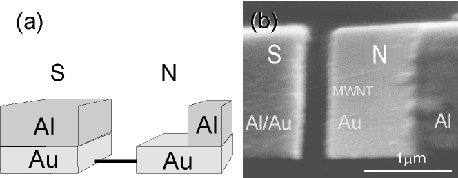
Here we report on electrical transport measurements of a Multi Wall Carbon Nanotube (MWNT) quantum dot connected to a normal and a superconducting lead. The sample is prepared as follows. First MWNTs are spread on a degenerately doped silicon substrate, in the experiment serving as a backgate, which is covered by a 400 nm insulating layer of SiO2. Then single nanotubes are contacted by means of standard electron-beam-lithography and e-gun-evaporation. Similar to reference [3] the superconducting contact is a 45 nm Au/ 160 nm Al proximity bilayer. However, by using tilt-angle-evaporation for the Al layer one obtains a structure such as the one sketched in figure 1(a). Whereas the left-hand side of the MWNT is coupled to the superconducting Au/Al bilayer, the right-hand electrode is formed simply by the 45 nm gold layer. There will also be Al deposited on this side, but the spatial separation of the nanotube-gold-contact and the Al film is fairly long (approximately 1 m). To check quantitatively whether also on this side of the sample proximity effects have to be taken into account one can estimate the Thoules energy [11]. The Thoules energy represents an upper limit in energy for observing superconducting correlations (assuming perfect barriers). One obtains eV mK using a gold diffusion constant m2/s (corresponding to an estimated Au mean free path of 10 nm) and a spatial separation L 1 m. The experiment is performed at mK, hence, is bigger than the estimated and any proximity induced superconductivity on the right sample contact can be safely neglected. Consequently the sample geometry represents a S-QD-N structure. Figure 1(b) shows an SEM (Scanning Electron Microscope) micrograph of the sample. Electrical transport measurements were performed in a Kelvinox dilution refrigerator.
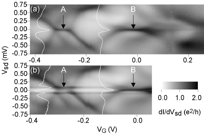
By applying a small perpendicular magnetic field of mT the superconducting electrode is driven into the normal state and the sample can be characterized in the N-QD-N configuration. This is possible because the magnetic field is bigger than the Aluminum critical field but still small in terms of the Zeeman shift of the nanotube energy levels ( where g 2 is the gyromagnetic ratio and the Bohr magneton). Figure 2(a) shows a greyscale representation of the differential conductance through the device at mK and mT with varying backgate and source-drain voltage. Despite some degree of disorder clear signs of Coulomb blockade diamonds and the Kondo effect as manifest in the high conductance ridges at zero bias voltage labelled “A” and “B” are visible. From the size of the diamonds one can deduce a charging energy 0.3 meV and a level spacing energy 0.3 meV. The coupling is of order 250. The Kondo effect occurs when the number of electrons on the dot is odd and it thus acts as a localized magnetic moment with spin 1/2. Below the Kondo temperature the spins of the leads try to screen the localized spin, i.e. change its spin expectation value to zero. In quantum dots this happens via fast spin-flip processes allowed only on a short timescale within the Heisenberg uncertainty principle. As a result of these processes between each lead and the dot a resonance of the dot spectral density at the chemical potential of the lead occurs which finally also causes a resonance of conductance at zero bias. In the so-called unitary limit for a perfectly transmitting transport channel opens up and the many-particle phenomenon Kondo effect reduces effectively to a completely non-interacting problem [10].
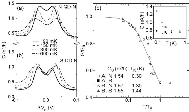
Figure 3(a) shows the temperature dependence of the linear conductance of ridge “A” for various temperatures in the normal state. can be determined by examining the temperature dependence of the linear conductance on the Kondo ridge, i.e. exactly in the middle of the two adjacent Coulomb peaks. As for the classical Kondo effect one finds a logarithmic temperature dependence. In order to determine we used the empirical relation where s=0.22 for a spin 1/2 system and the maximum conductance in the case of symmetric coupling [9]. Best fits to our data yield = 0.3 K, = 1.3 K, and . When plotting the normalized conductance over the reduced temperature the normal state data of ridges “A” and “B” collapse on a universal locus, as seen in figure 3(c). A further rough estimate of the Kondo temperature is obtained by the width of the resonant conductance peak yielding 0.6 meV ( 0.72 K) and 0.1 meV ( 1.2 K) for ridges “A” and “B”, respectively.
When one of the two electrodes enters the superconducting state the Kondo effect is modified. As was shown in [3] the Kondo effect is suppressed by superconductivity only when the superconducting gap is bigger than . A crossover is expected for . However, in contrast to an S-QD-S geometry here one faces an asymmetric situation and one has to distinguish the nature of coupling between the dot and the normal lead on one side and between the dot and the superconducting lead on the other. Whereas the Kondo processes between the normal lead and dot remain unaffected, two different scenarios are possible for the superconducting lead-dot-coupling. In a first case when is bigger than one expects the Kondo resonance to persist since quasiparticle states in the superconducting electrode can participate in the Kondo spin-flip processes. If, however, is smaller than these states will be missing and the Kondo coupling between the dot and the superconducting lead will be strongly suppressed. Yet a resonance of the dot spectral density with a renormalized Kondo temperature (Kondo resonance width) remains, which is caused by the Kondo processes between the normal lead and the dot. Whether one actually sees an enhancement of zero-bias conductance at temperatures below will now depend on the relevant dot energy scales such as the charging energy (suppresses Andreev reflections at the dot-superconductor interface) and the coupling strength on both sides and . In certain parameter regimes it thus should also be possible to enhance the conductance up to , which is the maximum value for a single perfectly-transmitting channel [12].
Figure 2(b) shows the conductance through our device in a greyscale representation for the superconducting state at T=90 mK and B=0 mT. The magnitude of the superconducting gap can be deduced from the horizontal feature at 0.09 meV in good agreement with [3], yielding a transition temperature K. For the energy scales of our quantum dot we thus obtain . We now focus on the two Kondo regions in the superconducting case. In the case of ridge “B” with the width of the Kondo resonance being bigger than the superconducting gap () both the greyscale plot and the temperature dependence of the Kondo conductance remain almost identical to the normal state, i.e. a strong zero-bias conductance resonance and a logarithmic temperature dependence at low temperatures. However, for temperatures approaching the transition temperature the conductance in the S-QD-N case is slightly higher than in the N-QD-N case, similar to what one would expect for a channel with constant transmission in the BTK model [13]. When fitting the temperature dependence with the same formula as above one obtains a slightly enhanced Kondo temperature of K and a slightly reduced maximum conductance of e2/h. For this fit we only considered temperatures sufficiently below in order to exclude the BTK-like conductance enhancement mentioned above. The data also collapse on the universal Kondo locus, see figure 3(c).
The resonance of ridge “B” remains in the superconducting state, but its conductance is not increased. At first sight this behavior seems surprising, since resonances indicate a high effective transmission for which a doubling in conductance is expected in the unitary limit. This, however, only holds for a symmetrically coupled junction. Our observation is in quantitative agreement with the theoretically expected conductance if we account for the asymmetry. We consider the unitary limit for which the results for non-interacting electrons should hold. The maximum conductance (at resonance) of a transport channel between two normal electrodes is given by . From our data we obtain and thus a relative asymmetry of the lead coupling of (or the inverse). Between a normal and a superconducting lead the maximum Andreev conductance has the form [12]. Using the -ratio determined before one obtains for the resonance conductance in the superconducting state . This value is only slightly higher than the one in the normal state and therefore explains our experimental observation.
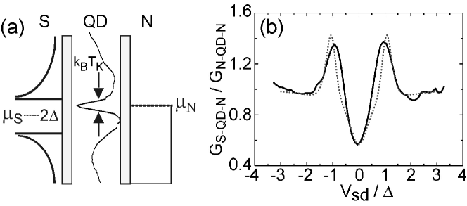
In case of ridge “A” the scenario is different (). The superconducting electrode results in a suppression of the zero bias Kondo conductance enhancement but high conducting side ridges at the position of the gap occur. This can be understood when taking a look at figure 4(a) where the electronic spectrum of the quantum dot and of the leads is depicted. The remaining Kondo coupling between the normal lead and the dot results in a resonance of the dot spectral density pinned to the normal lead chemical potential . At a bias of the superconductor quasiparticle spectrum and the normal lead chemical potential (and thus the Kondo resonant level) are lined up and resonant transport occurs. The linear conduction of ridge “A” in the superconducting state versus gate voltage is shown for various temperatures in figure 3(b). In the inset of figure 3(c) the conductance at the center of ridge “A” is plotted versus temperature for both the normal and the superconducting state. Whereas there is an increase of conductance below K for the normal state data, the conductance remains more or less constant in the superconducting case. Thus we were not able to perform a fit in order to determine the renormalized Kondo temperature . However, we suspect to be of the order of 100 mK since the 90 mK data show an increase of conductance. The temperature dependence of the conductance on the -side-peaks (data not shown) does not show logarithmic behavior down to our lowest temperatures either, but similar to the linear response conductance an enhancement for the 90 mK data. This might indicate Kondo coupling at non-zero bias between the quasiparticles in the superconducting and the normal lead.
The behavior of ridge “A” can find a simple explanation by assuming a strong suppression of the Kondo coupling between the dot and the superconducting lead lowering the effective transmission of this interface to values comparable to tunnel barriers. The current through our device in the superconducting state is then given by [14]:
| (1) |
with being the BCS density of states in the superconducting lead, the QD local density of states of the resonant level with width , the Fermi function and the transmission of the barrier. Similar to [15] we included a broadening of the BCS density of states which we attribute to the additional Au layer separating tube and Al layer. In figure 4(b) we plot the conductance of ridge “A” in the superconducting state normalized by that in the normal state from both our experimental data and simulations. Best agreements are obtained with , and . Finite temperature is taken into account by setting T=0.1. In the normal state we approximated the Kondo conductance peak as a Lorentzian. Comparison with our experimental data yields for the width of the Lorentzian , a maximum conductance of 1.35 and a background conductance of 0.75 . The proposed model clearly reproduces the main features of the experimental data, however precise quantitative agreement remains difficult. A possible explanation of e.g. the bigger width of the -peaks is an energy-dependent transmission matrix element (which we assumed to be constant) of increasing magnitude as the applied bias approaches due to Kondo coupling between the normal lead, the dot and the superconducting quasiparticles.
In this paper we studied a carbon nanotube quantum dot in the Kondo regime coupled to a normal and a superconductor. In the case of the Kondo ridge at zero bias disappears and peaks at the position of the gap occur. For this scenario we proposed a simple tunnelling model explaining all significant features of the conductance curves. In the case the Kondo resonance persists but does not show an enhancement of the conductance compared to the normal state at the lowest temperatures accessible in our experiment. Future experiments will have to (a) clarify whether the Kondo resonance can actually be enhanced in presence of the superconducting electrode by tuning the coupling asymmetry and (b) explore the possibility of generating pairs of entangled electrons by making use of nanotubes coupled to normal and superconducting leads [8].
We thank M. Buitelaar, B. Choi, L. Grueter, T. Kontos and S. Sahoo for experimental help and A. Clerk, J. Cuevas, T. Kontos, A. Levy Yeyati and P. Recher for discussions. We thank L. Forro for the MWNT material and J. Gobrecht for the oxidized Si substrates. This work has been supported by the Swiss NFS and the NCCR on Nanoscience.
References
References
- [1] J Nygard, H Cobden and P Lindelof Nature 342 (2000)
- [2] MR Buitelaar, A Bachthold, T Nussbaumer, M Iqubal and C Schönenberger Phys. Rev. Lett. 88 156801 (2002)
- [3] MR Buitelaar, T Nussbaumer and C Schönenberger Phys. Rev. Lett. 89 256801 (2002)
- [4] JC Cuevas, A Levy Yeyati and A Martin-Rodero Phys. Rev. B 63 094515 (2001)
- [5] A Clerk, V Ambegaokar and S Hershfield Phys. Rev. B 61 3555 (2000)
- [6] Q Sun, H Guo and T Lin Phys. Rev. Lett. 87 176601 (2001)
- [7] P Recher, EV Sukhorukov and D Loss Phys. Rev. B 63 165314 (2001)
- [8] P Recher and D Loss, Phys. Rev. B 65 165327 (2002); C Bena, S Vishveshwara, L Balents and MPA Fisher Phys. Rev. Lett. 89 037901 (2002); V Bouchiat, N Chtchelkatchev, D Feinberg, GB Lesovik, T Martin and J Torres Nanotechnology 14 77 (2003)
- [9] D Goldhaber-Gordon et alPhys. Rev. Lett. 81 5225 (1998)
- [10] L Kouwenhoven and L Glazman Phys. World 14 33-38 (2001)
- [11] S Gueron et alPhys. Rev. Lett. 77 3025 (1996)
- [12] CWJ Beenakker Phys. Rev. B 46 12841 (1992)
- [13] GE Blonder, M Tinkham and TM Klapwijk Phys. Rev. B 25 4515 (1982)
- [14] M Tinkham Introduction to Superconductivity McGraw-Hill (1996)
- [15] MR Buitelaar et alPhys. Rev. Lett. 91 057005 (2003)