Current induced spin polarization in strained semiconductors
Abstract
The polarization of conduction electron spins due to an electrical current is observed in strained nonmagnetic semiconductors using static and time-resolved Faraday rotation. The density, lifetime, and orientation rate of the electrically-polarized spins are characterized by a combination of optical and electrical methods. In addition, the dynamics of the current-induced spins are investigated by utilizing electrical pulses generated from a photoconductive switch. These results demonstrate the possibility of a spin source for semiconductor spintronic devices without the use of magnetic materials.
pacs:
72.25.Pn, 85.75.-d, 78.47.+pPreparation and control of spin information are key issues in the development of spintronics Wolf:2001 ; Semiconductor:2002 . The use of nonmagnetic semiconductors to electrically control electron spins has been demonstrated Salis:2001 ; Kato:2003 , even in the absence of magnetic fields Kato:2004 . An electrical means of preparing spin-polarized carriers without magnetic materials would provide a further step toward all-electrical nonmagnetic spintronic devices. It has been proposed that current-induced spin polarization may provide such an opportunity. The existence of a spin current perpendicular to a charge current, which would cause spin accumulation at the edges of a sample, has been predicted Dyakonov:1971 ; Hirsch:1999 ; Zhang:2000 ; Murakami:2003 . There also exist theories for spatially homogeneous spin polarization resulting from an electrical current in systems such as two dimensional electron gases Levitov:1985 ; Edelstein:1990 ; Aronov:1991 ; Magarill:2001 ; Chaplik:2002 ; Inoue:2003 ; Cartoixa:2001 ; Silsbee:2001 . It is anticipated that application of an electric field establishes an effective magnetic field which polarizes the electron spins. Experimental attempts to detect such polarization using ferromagnetic contacts have been made Hammer:1999 ; Hammer:2000 ; Hammer:2001 , but the local Hall effect and anisotropic magnetoresistance complicate these measurements Monzon:1999 ; van:1999 ; Hammer:2002 ; Monzon:2000 ; Filip:2000 .
Recently, it was found that strained semiconductors exhibit spin splitting in the presence of applied electric fields Kato:2004 . In this Letter, we report the optical detection of current-induced electron spin polarization in strained GaAs and InGaAs epitaxial layers. The high sensitivity of the optical Faraday rotation technique allows detection of 100 spins in an integration time of about a second, unambiguously revealing the presence of a small spin polarization due to laterally applied electric fields. We are able to extract quantitative values of spin density by comparing the Faraday rotation due to electric fields to that induced by optical spin injection. The spin orientation process persists up to a temperature K with no marked degradation of efficiency, and is also observed over picosecond timescales in time-resolved measurements in which a coherent spin population is excited with electrical pulses derived from a photoconductive switch.
The samples studied here are grown on (001) semi-insulating GaAs substrates by molecular beam epitaxy. Eight different heterostructures with strained In0.07Ga0.93As layers as well as strained GaAs membranes Kato:2004 were investigated. Qualitatively similar behavior has been seen in all samples, but for most of this Letter we will concentrate on devices fabricated from one of the wafers (sample E in Ref. Kato:2004 ) in order to avoid confusion. The heterostructure consists of 500 nm of -In0.07Ga0.93As (Si-doped for cm capped with 100 nm of undoped GaAs. The -InGaAs layer is strained due to the lattice mismatch Jain:1996 , and although strain relaxation can be seen, there exists residual strain as determined by reciprocal space mapping with an x-ray diffractometer at room temperature.
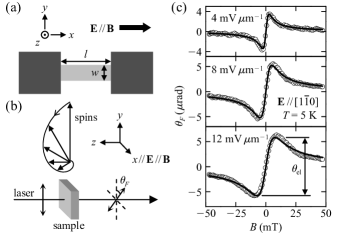
A schematic of a device is shown in Fig. 1(a). Photolithography and chemical wet etching are employed to form the -InGaAs mesa, and Ni/GeAu metallization followed by annealing is used to make ohmic contacts to the -InGaAs layer. Two such devices are fabricated on a chip to allow measurements with the electric field E along either of the two crystal directions [110] and . The sample is placed inside a magneto-optical cryostat with a variable temperature insert such that the magnetic field B is parallel to E. In order to probe the spin polarization in the sample, Faraday rotation is measured in the Voigt geometry [Fig. 1(b)]. A mode-locked Ti:sapphire laser operating at a repetition frequency MHz produces 150 fs pulses and is tuned to a wavelength nm. A linearly polarized probe beam with an average power of 130 W is directed along the axis, normally incident and focused on the sample. The polarization axis of the transmitted beam rotates by an angle that is proportional to the component of the spins Crooker:1997 , and the rotation angle is detected with a balanced photodiode bridge. A square-wave voltage with peak-to-peak value at frequency kHz is applied to one of the contacts while the other contact is grounded. An alternating electric field with amplitude is established along the InGaAs channel of width and length , assuming negligible contact resistance. The current-induced is lock-in detected at as a function of the applied magnetic field along the axis. Typical data are shown in Fig. 1(c), for three different electric fields.
The curves can be explained by assuming a constant orientation rate for spins polarized along the axis. In a manner similar to the case of optical orientation Optical:1984 under static illumination, the component of spin per unit volume can be written as
where is the number of spins oriented along the axis per unit time per unit volume, is the inhomogeneous transverse spin lifetime, is the electron Larmor frequency, is the steady-state spin density due to electrical excitation, is the effective electron g factor, is the Bohr magneton, and is the Planck constant. The upper integration limit is taken as infinity since the modulation period is much longer than , and the effective magnetic field observed in Kato:2004 is omitted as it is a second order effect due to its parallel orientation to the current-induced spins. Approximating the beam profiles as Gaussians, assuming spatially uniform , and letting be proportional to both and the intensity of the probe beam with a proportionality constant , we find
where is the thickness of the epitaxial film, is the peak intensity of the probe beam, and are the standard deviation of the laser intensity in the and directions, respectively, and is the amplitude of the electrically-induced . By fitting the data with the above equation, we obtain and . The data does not change significantly when the laser spot is moved across or along the channel, while polarization due to a spin current is expected to appear only within a spin diffusion length from the channel edge and reverse sign for opposing edges Dyakonov:1971 ; Hirsch:1999 ; Zhang:2000 ; Murakami:2003 . This suggests that the relevant mechanism is wave-vector dependent spin-splitting which predicts uniform polarization Edelstein:1990 ; Aronov:1991 ; Magarill:2001 ; Chaplik:2002 ; Inoue:2003 ; Cartoixa:2001 ; Silsbee:2001 .
Additional quantitative analysis can be performed by measuring time-resolved Faraday rotation (TRFR) Crooker:1997 in the absence of electric fields with the same probe power. In this measurement, a circularly polarized pump beam (13 W, nm) is focused onto an overlapping spot with the probe beam, optically injecting electron spins Optical:1984 . The time delay between the pump pulse and the probe pulse is adjusted by a mechanical delay line, and the pump beam helicity is modulated at 50.1 kHz with a photoelastic modulator for lock-in detection. In the presence of an applied magnetic field, oscillates as a function of with frequency , from which can be determined Crooker:1997 . Measurement at T gives , which is used to obtain from the fits to the voltage-induced Faraday rotation data. Furthermore, can be extracted by comparing to the optically induced . Just after the pump pulse, the spin density profile should track the pump beam intensity profile, and the Faraday rotation is
| (neV ns m111Sample details and original data on given in reference Kato:2004 . | (m-2 V-1 ns | |||||||||||||||||||||||
| Sample111Sample details and original data on given in reference Kato:2004 . | [110] | [110] | ||||||||||||||||||||||
| GaAs | + | 99 | + | 216 | ( | + | 92 | 67 | ) | |||||||||||||||
| B | 13 | 39 | 35 | ( | + | 13 | 22 | ) | + | 4 | ( | + | 2 | 1 | ) | |||||||||
| C | + | 44 | 21 | 15 | ( | + | 7 | 26 | ) | + | 65 | ( | + | 113 | 32 | ) | ||||||||
| D | + | 125 | + | 4 | + | 4 | ( | + | 20 | 2 | ) | + | 30 | ( | + | 158 | 17 | ) | ||||||
| E | + | 112 | + | 27 | 61 | ( | + | 19 | 27 | ) | + | 422 | ( | + | 185 | 133 | ) | |||||||
| F | + | 84 | + | 23 | + | 75 | ( | + | 19 | 28 | ) | + | 216 | ( | + | 143 | 81 | ) | ||||||
| G | + | 75 | + | 13 | + | 25 | ( | + | 20 | 10 | ) | + | 36 | ( | + | 28 | 14 | ) | ||||||
| H | + | 23 | 26 | 64 | ( | + | 23 | 40 | ) | + | 84 | ( | + | 52 | 31 | ) | ||||||||
| I | + | 89 | + | 42 | + | 7 | ( | + | 4 | 2 | ) | + | 25 | ( | + | 14 | 9 | ) | ||||||
where is the peak spin density due to the pump beam and is the optically induced . In Fig. 2(a), TRFR data at early time is shown. Initial rapid decay is attributed to the presence of holes and/or excitons Kikkawa:1997 , and since their contribution to is unknown, the value used for is an average of the maximum at and the value extrapolated back to from the data points after the rapid decay. These two values were also used to set the bounds on . Assuming 50% polarization from circularly polarized light Optical:1984 , the total number of optically injected spins per pulse is , where is the absorbed power of the pump beam and is the speed of light. The reflected and the transmitted power of the pump beam are measured on and off the InGaAs mesa in order to determine , while and are obtained from measurement of as a function of pump-probe spatial distance [Fig. 2(a) inset] using a stepper-motor-driven mirror Kato:2004 . Taking signal convolution into account, normalized data are fit to to give m and m. We estimate 20 % error in the determination of . Finally, and are obtained.
As expected, increases with [Fig. 2(b)] and reaches 8 m-3, corresponding to a spin polarization of , while decreases with [Fig. 2(c)], leading to the saturation of . An approximately linear relation between and is seen [Fig. 2(d)], and we define the spin orientation efficiency as the slope of a linear fit to versus The slight nonlinearity seen for small may be due to the current-voltage characteristics of the device not being perfectly linear. The sign of is determined from current-induced nuclear polarization in EB geometry, measured by Larmor magnetometry Salis:2002 . We note that is more positive when E//, consistent throughout the eight heterostructures investigated (Table 1). Although theories for two-dimensional electron gas predict a proportional relation between spin-splittings and Edelstein:1990 ; Aronov:1991 ; Magarill:2001 ; Chaplik:2002 ; Inoue:2003 ; Cartoixa:2001 , we observe sign contradictions in some cases.
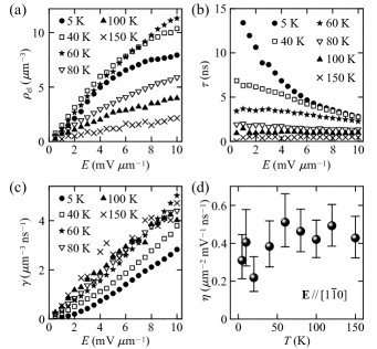
In Fig. 3, we explore the temperature dependence of the effect. At each , is adjusted to optimize the Faraday rotation signal due to optically injected spins, and the set of measurements is repeated. At temperatures above 80 K, becomes smaller [Fig. 3(a)] due to the decline of [Fig. 3(b)]. It is seen that and do not considerably change up to K [Fig. 3(c) and Fig. 3(d)]. The signal is below the noise level for K due to shorter and lower sensitivity of Faraday rotation.
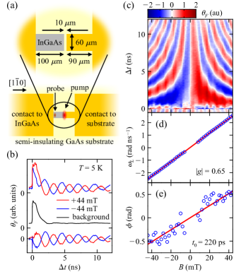
In order to investigate the effect at shorter timescales, we employ a two-color pump-probe setup Kikkawa:1997 in conjunction with a photoconductive switch Auston:1983 to produce electrical pulses [Fig. 4(a)]. The pump beam (2.8 mW) is linearly polarized to avoid optical spin injection, and is tuned to nm in order to excite carriers in the GaAs substrate. The photoexcited carriers temporarily short the two contacts, thus producing an electrical pulse whose duration is limited by the carrier lifetime. The probe beam (130 W, nm) is placed 90 m from the pump beam. A square-wave with V at Hz is applied on the contact to the InGaAs layer, and the contact to the substrate is grounded. The pump beam is chopped at kHz and the signal is lock-in detected at . The time evolution of voltage-induced at mT is shown in Fig. 4(b), demonstrating current-induced electron spin polarization at these timescales. The sign of the signal reverses with the direction of , as expected for in-plane excitation of spins. There exists a non-oscillating -independent signal in addition to the oscillating component, which can be extracted by averaging the data over a range of . This background may be an absorption signal arising from excess carriers, detected due to an imperfect balancing of the photodiode bridge. We subtract the background for analysis, and the data after subtraction are plotted at the bottom of Fig. 4(b). Such data taken for a range of are plotted in Fig. 4(c). The weak amplitude ripples along the axis are due to resonant spin amplification Kikkawa:1998 . We fit each versus t curve to , where is the initial amplitude and is the phase. We obtain from the slope of [Fig. 4(d)], consistent with measurements using optical spin injection, thus confirming that the voltage-induced signal arises from electron spins. There also exists a slope to [Fig. 4(e)] due to the time delay ps between the pump pulse and the spin excitation, which we attribute to the width of the electrical pulse.
The presented results demonstrate electron spin polarization due to an electrical current in strained semiconductors, generating possibilities for spintronic devices in which spin initialization and manipulation are performed without magnetic materials or magnetic fields. Larger spin polarization may be achievable in narrow gap semiconductors and two-dimensional quantum structures where the spin-orbit effects are larger.
Acknowledgements.
We acknowledge support from DARPA SPINS and QuIST programs, and the DMEA.References
- (1) S. A. Wolf et al., Science 294, 1488 (2001).
- (2) Semiconductor Spintronics and Quantum Computation, edited by D. D. Awschalom, D. Loss, and N. Samarth (Springer-Verlag, Berlin, 2002).
- (3) G. Salis et al., Nature 414, 619 (2001).
- (4) Y. Kato et al., Science 299, 1201 (2003).
- (5) Y. Kato, R. C. Myers, A. C. Gossard, and D. D. Awschalom, Nature 427, 50 (2004).
- (6) M. I. Dyakonov and V. I. Perel, Phys. Lett. A 35, 459 (1971).
- (7) J. E. Hirsch, Phys. Rev. Lett. 83, 1834 (1999).
- (8) S. Zhang, Phys. Rev. Lett. 85, 393 (2000).
- (9) S. Murakami, N. Nagaosa, and S. C. Zhang, Science 301, 1348 (2003).
- (10) L. S. Levitov, Y. V. Nazarov, and G. M. Eliashberg, Sov. Phys. JETP 61, 133 (1985).
- (11) V. M. Edelstein, Solid State Commun. 73, 233 (1990).
- (12) A. G. Aronov, Y. B. Lyanda-Geller, and G. E. Pikus, Sov. Phys. JETP 73, 537 (1991).
- (13) L. I. Magarill, A. V. Chaplik, and M. V. Entin, Semiconductors 35, 1081 (2001).
- (14) A. V. Chaplik, M. V. Entin, and L. I. Magarill, Physica E 13, 744 (2002).
- (15) J. Inoue, G. E. W. Bauer, and L. W. Molenkamp, Phys. Rev. B 67, 33104 (2003).
- (16) X. Cartoixa, D. Z. Y. Ting, E. S. Daniel, and T. C. McGill, Superlattices Microstruct. 30, 309 (2001).
- (17) R. H. Silsbee, Phys. Rev. B 63, 155305 (2001).
- (18) P. R. Hammer, B. R. Bennett, M. J. Yang, and M. Johnson, Phys. Rev. Lett. 83, 203 (1999).
- (19) P. R. Hammer and M. Johnson, Phys. Rev. B 61, 7207 (2000).
- (20) P. R. Hammer and M. Johnson, Appl. Phys. Lett. 79, 2951 (2001).
- (21) F. G. Monzon, H. X. Tang, and M. L. Roukes, Phys. Rev. Lett. 84, 5022 (1999).
- (22) B. J. van Wees, Phys. Rev. Lett. 84, 5023 (1999).
- (23) P. R. Hammer, B. R. Bennett, M. J. Yang, and M. Johnson, Phys. Rev. Lett. 84, 5024 (1999).
- (24) F. G. Monzon and M. L. Roukes, J. Mag. Mag. Mat. 198-199, 632 (1999).
- (25) A. T. Filip et al., Phys. Rev. B 62, 9996 (2000).
- (26) S. C. Jain, M. Willander, and H. Maes, Semicond. Sci. Technol. 11, 641 (1996).
- (27) S. A. Crooker et al., Phys. Rev. B 56, 7574 (1997).
- (28) Optical Orientation, edited by F. Meier and B. P. Zakharchenya (Elsevier, Amsterdam, 1984).
- (29) J. M. Kikkawa, I. P. Smorchkova, N. Samarth, and D. D. Awschalom, Science 277, 1284 (1997).
- (30) G. Salis, D. D. Awschalom, Y. Ohno, and H. Ohno, Phys. Rev. B 64, 195304 (2001).
- (31) D. H. Auston, IEEE J. Quant. Electron. QE-19, 639 (1983).
- (32) J. M. Kikkawa and D. D. Awschalom, Phys. Rev. Lett. 80, 4313 (1998).