Rashba Effect at Magnetic Metal Surfaces
Abstract
We give experimental and theoretical evidence of the Rashba effect at the magnetic rare-earth metal surface Gd(0001). The Rashba effect is substantially enhanced and the Rashba parameter changes its sign when a metal-oxide surface layer is formed. The experimental observations are quantitatively described by ab initio calculations that give a detailed account of the near-surface charge density gradients causing the Rashba effect. Since the sign of the Rashba splitting depends on the magnetization direction, the findings open up new opportunities for the study of surface and interface magnetism.
pacs:
71.70.Ej, 72.25.-b, 73.20.-r, 85.75.-dA key issue in condensed-matter research aiming at future spintronic devices Wolf et al. (2001) is to control and manipulate the electron spin in a two-dimensional electron gas (2DEG) of semiconductor systems without the need of applying an external magnetic field. Rashba had realized early on Rashba (1960) that this can be achieved by an electric field which acts as a magnetic field in the rest frame of a moving electron. The interaction between the spin of a moving electron of momentum with an electric field oriented along the -axis is described by the Rashba Hamiltonian
| (1) |
The Rashba parameter is proportional to the electric field and depends on the effective, material-dependent spin-orbit coupling (SOC) strength. In nonmagnetic systems the Rashba effect lifts the spin-degeneracy of the energy dispersion of an electronic state, and the energy difference between and is called Rashba splitting . Even though spintronic research currently focuses on spin-polarized electrons in semiconductors Zhu et al. (2001); Jiang et al. (2003), it is important to explore the Rashba effect in other material classes as well.
A necessary condition for the Rashba effect to occur is the absence of inversion symmetry and, while in the proposed FET-type spin transistor Datta and Das (1990) a gate voltage must be applied to break inversion symmetry of the 2DEG, this condition is naturally fulfilled by the structural inversion asymmetry (SIA) existing at any crystal surface or interface. Owing to SIA, electrons in a two-dimensional surface or interface state experience an effective crystal potential gradient perpendicular to their plane of propagation, hereby optimizing in Eq. (1). One should expect that the Rashba effect is a general surface and interface phenomenon, but up to now Rashba splittings have only been observed for surface states at Au(111) LaShell et al. (1996); Reinert et al. (2001) and W(110) Rotenberg and Kevan (1998); Hochstrasser et al. (2002). Recently relativistic density functional theory (DFT) calculations were able to reproduce the observed splitting of the Au -like surface state Nicolay et al. (2001) and the analogy to a 2DEG has been pointed out Henk et al. (2003). Yet, it is still a challenging task to give a physical picture of the Rashba effect from the electronic structure point of view.
This Letter presents the first experimental and theoretical evidence of a Rashba splitting of exchange-split two-dimensional electron states. Using the surface state of ferromagnetic Gd metal as example we report on the novel finding of a k-dependent contribution to the binding energy of this state that changes sign upon magnetization reversal. It is further demonstrated that the Rashba effect is enhanced upon formation of a surface oxide layer. The experimental observations are quantitatively described by ab initio calculations showing that the enhancement is caused by a substantial change of charge-density gradients at the interface between the surface-oxide layer and the bulk-like metal, which leads to an admixture of character to the -derived two-dimensional state.
In particular, we show that the Rashba effect in magnetic systems bears interesting consequences when the spin-degeneracy of is already lifted by an exchange splitting , separating majority () and minority () electrons. The dispersion of a state subject to the Rashba effect can then be written as and the Rashba splitting can be observed separately for majority and minority states by two subsequent measurements with opposite sample magnetization, and . Since in many cases the Rashba splitting is non-zero only for surface and interface states, the observation of this quantity opens a new and powerful spectroscopic path to discriminate surface and interface magnetism from bulk magnetism.
For the present investigation we chose the (0001) surface of ferromagnetic hcp Gd metal where the exchange interaction is known to separate majority and minority branches of the -derived surface state by several hundred meV Weschke et al. (1996). With this substantial exchange splitting a limitation in previous studies of non-magnetic systems is avoided, where the Rashba splitting of a state, in order to be resolved, must be larger than its intrinsic (lifetime) width Reinert et al. (2001). The remanent in-plane magnetization of thin Gd(0001) films Berger et al. (1994) means that the spin-quantization axis is orthogonal to the surface electric field, providing an advantageous geometry for observing a Rashba splitting, see Eq. (1). The O/Gd(0001) surface oxide allows furthermore to study an exchange-split pair of two-dimensional states Schüssler-Langeheine et al. (1999) that are both occupied.
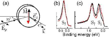
Angle-resolved photoemission (PE) experiments were performed using display-type electron analyzers at the I-311 undulator beamline at MAX-Lab, Lund, and at the BUS beamline at BESSY, Berlin. In the experiments, the energy resolution was set to 30 meV and the angular resolution to . Gd(0001) films were prepared by metal vapor deposition on a W(110) single crystal mounted on a liquid-He flow cryostat. The film thickness was 10 nm as determined by a quartz balance. During evaporation the pressure in the UHV chamber rose from mbar to mbar. The surface monoxide layer was prepared according to the recipe given in Ref. Schüssler-Langeheine et al. (1999) with 2 Langmuir oxygen exposure; it was controlled in situ by PE and LEED. The PE spectra were recorded from remanently magnetized samples in the experimental geometry shown in Fig. 1(a).
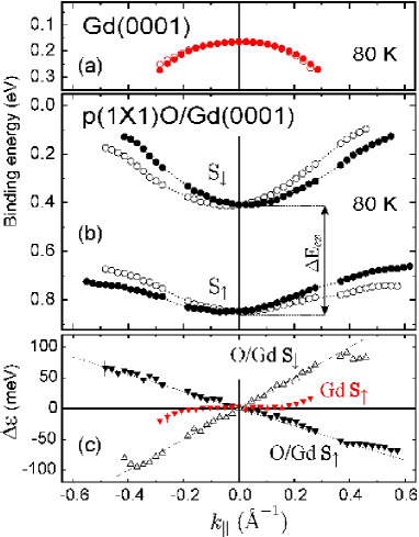
For ferromagnetic Gd metal only the majority component of the -derived Gd(0001) surface state is occupied Weschke et al. (1996), as is shown by the angle-resolved PE spectrum in Fig. 1(b). At off-normal emission angles, the peak position shifts significantly upon magnetization reversal. Derived from experimental spectra, the dispersion near the center of the surface Brillouin zone along the - direction is presented in Fig. 2(a); filled and open data points distinguish the two branches measured for opposite magnetization directions (cf. Fig. 1(a)). The branches are shifted symmetrically with respect to , in agreement with the triple-vector product of Eq. (1). The energy difference is plotted in Fig. 2(c). It is identified as Rashba splitting of the Gd(0001) surface state; it remains rather small ( meV) in the range of .
The O/Gd(0001) surface oxide exhibits an exchange-split pair of surface bands Schüssler-Langeheine et al. (1999) that are both occupied, shown as and in Fig. 1(c). For nonzero (off-normal emission), the peak positions clearly change into opposite directions when the magnetization is reversed. Their (upward) dispersions are shown in Fig. 2(b): they change symmetrically with respect to the Brillouin zone center, strongly supporting our interpretation as Rashba splitting. The energy splitting is plotted separately for S↑ and S↓ in Fig. 2(c); it is substantially larger (about three times at ) than the Rashba splitting of the majority surface state on Gd(0001). Moreover, the Rashba parameters for the oxide-covered and the clean metal surface are found to have opposite signs, see Fig. 2(c). – We note in passing that for O/Gd(0001) also the modulus of the slopes, , is different for and .
The ab initio calculations were performed using DFT in the local density approximation (LDA) employing the form of Moruzzi et al. Moruzzi et al. (1978). We use the full-potential linearized augmented-plane-wave method in film geometry Wimmer et al. (1981); www , with SOC included self-consistently according to Ref. Li et al. (1990). For a proper description of the electrons we applied the LDA+U method Kurz et al. (2002). The Gd surface was simulated by a structurally relaxed 10-layer film embedded in two semi-infinite vacua. A plane-wave cutoff of (a.u.)-1 was used, and the irreducible part of the two-dimensional Brillouin-zone (BZ) was sampled at 21 special points (36 points for calculations with SOC included).
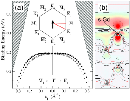
In the calculations with SOC included, we took into account that the in-plane magnetization lowers the symmetry of hcp Gd to symmetry. One can still label the high symmetry points of the BZ as and , but with subscripts to distinguish between inequivalent points, see Fig. 3(a). Points that are related by an inversion center are primed to indicate that the bandstructure is equivalent to the unprimed -points if one interchanges spin-up and spin-down bands. The magnetization was assumed to point in the direction of the in-plane nearest neighbors. The size of the Rashba splitting decreases from the - direction to - and further to -, and is zero in - direction.
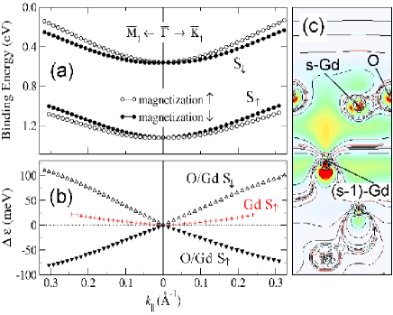
The theoretical results for O/Gd(0001) are presented in Fig. 4. In the calculation, the O atoms were ’adsorbed’ on the fcc site and its relaxed position was found 0.78 Å above the plane of Gd surface atoms, s-Gd. Upon O adsorption, the s-Gd layer shows a strong (18%) outward relaxation, while the position of the inner layers remains almost unperturbed. Very similar results were obtained for O adsorbed on the energetically slightly less favorable hcp site. In Fig. 4(a), the two occupied states disperse upwards (positive effective mass) in good agreement with experiment, see Fig. 2. (The exchange splitting is somewhat larger than the experimental value, an overestimation that had been noted before for clean Gd(0001) Kurz et al. (2002).) The calculated Rashba splitting of majority-spin and minority-spin bands is shown in Fig. 4(b); it is about three times larger than that of the Gd(0001) metal surface, and is found to be of opposite sign, in excellent agreement with experiment.
With the results of the present ab initio calculations, we can address the question why the oxide layer on Gd(0001) causes an enhanced Rashba splitting. Figs. 3(b) and 4(c) display the charge density distributions of the two-dimensional states at for the two systems, Gd metal and O/Gd, in a plane perpendicular to the surface. In addition to the conventional isolines (log scale), the surface-state charge densities are also given on a linear scale (color) for better visibility. When comparing the profiles it becomes obvious that adsorption of the electronegative O atom changes the charge density distribution of the entire near-surface region. While the surface state of the metal surface, cf. Fig. 3(b), resides almost exclusively (to %) in the top surface layer s-Gd, the two-dimensional state in O/Gd is distributed over both the s-Gd and ()-Gd layer, see Fig. 4(c). Hence, given the close vicinity of O and s-Gd layer, this state may be conceived as interface state located between a O/Gd surface monoxide layer and bulk-like Gd metal.
At Gd(0001) the surface-state charge is located quite symmetrically below and above the s-Gd plane, cf. Fig. 3(b), corresponding to a small (positive) charge density gradient along the surface normal. The small charge density gradient directly indicates that there is a small electric field in the s-Gd layer of Gd(0001), which gives rise to the small Rashba splitting, shown in Figs. 2(c) and 4(b). At O/Gd(0001), by contrast, the rather asymmetric charge distribution of the interface state in the ()-Gd layer directly indicates the presence of a high effective electric field at this layer. The charge gradient is negative, i.e. opposite to the uncovered metal surface. We are led to conclude that it is this reversed effective electric field in the ()-Gd layer that causes the opposite sign of the Rashba parameter of the interface state in O/Gd(0001) as compared with Gd(0001).
Furthermore, the calculations reveal that the surface oxide formation is accompanied by a pronounced change in orbital character of the two-dimensional state. In the s-Gd layer it changes upon oxidation from almost exclusively -like (-ratio , integrated over the muffin-tin sphere) to predominantly -like with an admixture of other orbital components (). In the ()-Gd layer of O/Gd the state remains -like yet with a substantial -admixture (). Moreover, in order to identify the relative contributions of the individual layers to the Rashba splitting, we calculated hypothetical values of the splitting with SOC set to zero for all other layers. Again there is a striking difference of the two systems: at Gd(0001), the s-Gd layer provides by far the main contribution (%) to the Rashba splitting; yet in the surface oxide system it is the ()-Gd layer that accounts for over 70% of the splitting, whereas the s-Gd layer of O/Gd cannot contribute owing to its prevailing s character (see above).
In the light of these results we arrive at the following physical picture of the Rashba effect. At the Gd(0001) metal surface SIA leads to a small but significant spill-out of the -derived surface state, yet the charge gradient is small indicated by the relatively small admixture of -character (antisymmetric w.r.t. the surface plane) to the -derived state. With the epitaxial O/Gd surface oxide layer present, the electronegative O attracts charge from the s-Gd atom so that strong charge-density gradients arise not only in the s-Gd layer but also in the sub-surface layer. As a consequence, the two-dimensional state changes in spatial distribution (becoming an interface state) and in orbital character.
In summary, we have demonstrated that in magnetic systems with sufficiently large exchange splitting, , i.e. when majority () and minority spin () electronic states are well separated, even small Rashba splittings can be determined by two subsequent measurements with opposite sample magnetizations. Since one can expect an analogous behavior for other magnetic materials, a measurement of the Rashba splitting opens up a new and powerfull way to discriminate surface and interface magnetism from bulk magnetism. The present discovery of a particularly large Rashba effect at an interface between a two-dimensional metal oxide and a magnetic metal should stimulate future research towards a potential use of such interfaces for spintronic devices. – Moreover, based on the present findings it appears to be particularly interesting to study the evolution of an exchange-split two-dimensional state into a laterally confined quantum-well state of a magnetic nanostructure where the elastic reflection of the state is suppressed owing to the Rashba effect, since the reflected state is energetically not accessible.
We gratefully acknowledge expert experimental support by J. Andersen (MAX-Lab) and R. Püttner (BUS beamline, BESSY). The work in Berlin was supported by BMBF, Contract 05 KS1 KEC/2, and DFG (SfB-290).
∗Corresponding author: starke@physik.fu-berlin.de
References
- Wolf et al. (2001) S. A. Wolf, D. D. Awschalom, R. A. Buhrman, J. M. Daughton, S. von Molnar, A. Y. C. M. L. Roukes, and D. M. Treger, Science 294, 1488 (2001).
- Rashba (1960) E. I. Rashba, Sov. Phys. Solid State 2, 1109 (1960).
- Zhu et al. (2001) H. J. Zhu, M. Ramsteiner, H. Kostial, M. Wassermeier, H. P. Schönherr, and K. H. Ploog, Phys. Rev. Lett. 87, 016601 (2001).
- Jiang et al. (2003) X. Jiang, R. Wang, S. van Dijken, R. Shellby, R. Macfarlane, G. S. Solomon, J. Harris, and S. S. P. Parkin, Phys. Rev. Lett. 90, 256603 (2003).
- Datta and Das (1990) S. Datta and B. Das, Appl. Phys. Lett. 56, 665 (1990).
- LaShell et al. (1996) S. LaShell, B. A. McDougall, and E. Jensen, Phys. Rev. Lett. 77, 3419 (1996).
- Reinert et al. (2001) F. Reinert, G. Nicolay, S. Schmidt, D. Ehm, and S. Hüfner, Phys. Rev. B 63, 115415 (2001).
- Rotenberg and Kevan (1998) E. Rotenberg and S. D. Kevan, Phys. Rev. Lett. 80, 2905 (1998).
- Hochstrasser et al. (2002) M. Hochstrasser, J. G. Tobin, E. Rotenberg, and S. D. Kevan, Phys. Rev. Lett. 89, 216802 (2002).
- Nicolay et al. (2001) G. Nicolay, F. Reinert, S. Hüfner, and P. Blaha, Phys. Rev. B 65, 033407 (2001).
- Henk et al. (2003) J. Henk, A. Ernst, and P. Bruno, Phys. Rev. B 68, 165416 (2003).
- Weschke et al. (1996) E. Weschke, C. Schüssler-Langeheine, R. Meier, A. V. Fedorov, K. Starke, F. Hübinger, and G. Kaindl, Phys. Rev. Lett. 77, 3415 (1996).
- Berger et al. (1994) A. Berger, A. W. Pang, and H. Hopster, J. Magn. Magn. Mater. 137, L1 (1994).
- Schüssler-Langeheine et al. (1999) C. Schüssler-Langeheine, R. Meier, H. Ott, Z. Hu, C. Mazumdar, A. Y. Grigoriev, G. Kaindl, and E. Weschke, Phys. Rev. B 60, 3449 (1999).
- Moruzzi et al. (1978) V. Moruzzi, J. Janak, and A. Williams, Calculated Electronic Properties of Metals (Pergamon, New York, 1978).
- Wimmer et al. (1981) E. Wimmer, H. Krakauer, M. Weinert, and A. Freeman, Phys. Rev. B 24, 864 (1981).
- (17) For program description see http://www.flapw.de.
- Li et al. (1990) C. Li, A. J. Freeman, H. J. F. Jansen, and C. L. Fu, Phys. Rev. B 49, 5433 (1990).
- Kurz et al. (2002) P. Kurz, G. Bihlmayer, and S. Blügel, J. Phys.: Cond. Matter 14, 6353 (2002).