[
Charging induced asymmetry in molecular conductors
Abstract
We investigate the origin of asymmetry in various measured current-voltage (I-V) characteristics of molecules with no inherent spatial asymmetry, with particular focus on a recent break junction measurement. We argue that such asymmetry arises due to unequal coupling with the contacts and a consequent difference in charging effects, which can only be captured in a self-consistent model for molecular conduction. The direction of the asymmetry depends on the sign of the majority carriers in the molecule. For conduction through highest occupied molecular orbitals (i.e. HOMO or p-type conduction), the current is smaller for positive voltage on the stronger contact, while for conduction through lowest unoccupied molecular orbitals (i.e. LUMO or n-type conduction), the sense of the asymmetry is reversed. Within an extended Hückel description of the molecular chemistry and the contact microstructure (with two adjustable parameters, the position of the Fermi energy and the sulphur-gold bond length), an appropriate description of Poisson’s equation, and a self-consistently coupled non-equilibrium Green’s function (NEGF) description of transport, we achieve good agreement between theoretical and experimental I-V characteristics, both in shape as well as overall magnitude.
pacs:
PACS numbers: 85.65.+h, 73.23.-b,31.15.Ar]
Future electronic devices are quite likely to incorporate molecular components, motivated by their natural size, mechanical flexibility and chemical tunability. Encouraging progress in this direction has been achieved with the capacity to self-assemble, functionalize and reproducibly measure the current-voltage (I-V) characteristics of small groups of molecules. Molecular I-Vs reveal a wide range of conducting properties, from metallic conduction in carbon nanotubes [1] and quantum point contacts [2], to semiconducting behavior in DNA [3] and conjugated aromatic thiols [4], and insulating behavior in alkylthiol chains [5]. Interesting device characteristics such as rectification [6], switching [7] and negative differential resistance on silicon substrate [8] have also been reported. In particular, molecular rectification continues to be a widely studied property, right from the earliest days of this field.
The classic paradigm for asymmetry in molecular I-V measurements is the Aviram-Ratner diode, consisting of a semi-insulating molecular species bridging an electron donor-acceptor pair [9]. A positive bias on the contact at the donor end brings the energy levels on the donor and acceptor sites into resonance, while the opposite bias moves the system away from resonance, leading to a strongly asymmetric I-V characteristic [6]. Another example of asymmetric I-V is when the electrostatics of the system is dominated by one contact, e.g., a gated molecule where the gate is electrically connected to the source electrode [10, 11]. This gives rise to a spatially asymmetric electrostatic potential over the molecule which in turn generates a strong asymmetry in the I-V. In these, as well as most commonly studied examples of rectification, some kind of spatial asymmetry in the system seems essential, causing the energy levels, the electrostatic potential and the electron wave functions to be quite different for positive and negative voltages [12]. Typically, such asymmetry leads to peaks of similar heights in the conductance-voltage (G-V) characteristic occurring at different bias values.
In this paper, we address an I-V asymmetry observed for a spatially symmetric molecule [13, 14, 15] that is qualitatively different from and weaker than the rectifications in the above mentioned situations. The molecular I-V curves for these systems start off being symmetric, but pick up a weak, reversible asymmetry as the contacts are manipulated. In contrast to the two cases of rectification mentioned above, conduction in these molecules at opposite voltages occurs essentially through the same molecular levels with very similar wave functions. For resonant conduction in particular, this asymmetry shows up as conductance peaks of different heights occurring at symmetrically disposed voltage values. We show that the origin of the observed contact-induced asymmetry is nontrivial, and involves self-consistent shifts in the energy levels due to charging effects. Asymmetry in charging arises due to unequal coupling with the contacts, and seems to be present in conduction measurements performed with a break junction [13] or an STM tip [15].
Although this work addresses the origin of a weak rectification effect that may or may not be of practical significance from a device point of view, it serves three additional purposes: (a) using a computationally inexpensive yet rigorous self-consistent transport model we show the significance of charging effects in explaining experimentally observed I-V characteristics; (b) our calculated I-V (Fig. 1) is not just qualitatively, but also quantitatively in agreement with break-junction measurements on very small groups of molecules [13]. This is a significant deviation from the typical situations where theoretical estimates of current values differ from experimental currents by orders of magnitude [16, 17, 18, 19]; (c) the physics also sheds light on the nature of the charge carriers, i.e. whether conduction is n-type or p-type. The identification of the polarity of charge carriers is of obvious importance in semiconductor devices, since electrons and holes have different effective masses, leading to different mobilities. By analogy, molecular LUMO and HOMO levels have quite different wavefunctions [20], leading to different transmissions and current conducting properties. Much uncertainty exists about the nature of the conduction orbitals, or equivalently, the position of the Fermi energy relative to the molecular energy levels [17, 16, 19, 21, 22]. We argue that for the kind of contact-induced asymmetry discussed here, current is lower for positive bias on the strongly coupled contact for HOMO conduction, and higher if conduction is through a LUMO level.
A description of molecular conduction can be put on a quantitative footing by using an appropriate molecular Fock matrix (ab-initio or semi-empirical), coupled with a non-equilibrium Green’s function (NEGF) formulation of transport [17, 23]. For a given Fock matrix , overlap matrix , and contact self-energies with corresponding broadenings , the energy levels are given by the poles of the nonequilibrium Green’s function , while their occupancies are obtained from the corresponding density matrix , the contact electrochemical potentials and the Fermi functions :
| (1) | |||||
| (2) | |||||
| (3) |
The number of electrons and the steady-state current are then given by:
| (4) | |||||
| (5) |
where the transmission is given by:
| (6) |
It has been pointed out that the nature of the molecular I-V could sensitively depend on the self-consistent potential profile [24]. In our calculations, the self-consistent charging effect is included within an extended Hückel (EHT) [24, 20] description of the Fock matrix F, coupled with the NEGF equations described above. The self energies are calculated for Au (111) contacts in EHT using a recursive technique [20]. Both charging and screening effects are incorporated in F through a self-consistent potential which describes the potential profile of the molecule under applied bias:
| (7) |
where represents the change in density matrix under bias, . Equations (1) and (4) are then solved self-consistently to obtain the converged Fock matrix F. Any asymmetry in the potential profile is included explicitly in the self-consistent potential .
The Poisson part in equation (4) is approximated using the CNDO (complete neglect of differential overlap) method [25, 26], of which only the Hartree potential is being utilized in our treatment. Both charging and screening effects are incorporated into this term. In CNDO approximation, this Poisson term becomes:
| (8) | |||||
| (9) | |||||
| (10) | |||||
| (11) | |||||
| (12) | |||||
| (13) |
The notations used in Equation (5) are consistent with [26]. The two electron integrals ’s, are the CNDO parameters which are obtained from the experimental data and empirical fitting. These CNDO parameters allow us to capture the main physical characteristics of the e-e interaction without evaluating the computationally expensive two electron integrals directly.
The Laplace and image potentials are calculated by using a finite element method [27] treating the atomic sites as points in free space. The two electrodes are treated as metallic plates [100 100 ] separated by the molecular length. The molecule is placed in between the two plates. The Laplace part is then obtained by solving Laplace’s equation in 3D with the boundary conditions set by (: applied bias). The image part is calculated similarly but with different boundary conditions set by the potentials on the metallic plates due to point charges on the atomic sites. The inclusion of image potential in our model does not make any significant differences other than lowering the charging energy of the system by around 0.1 eV.
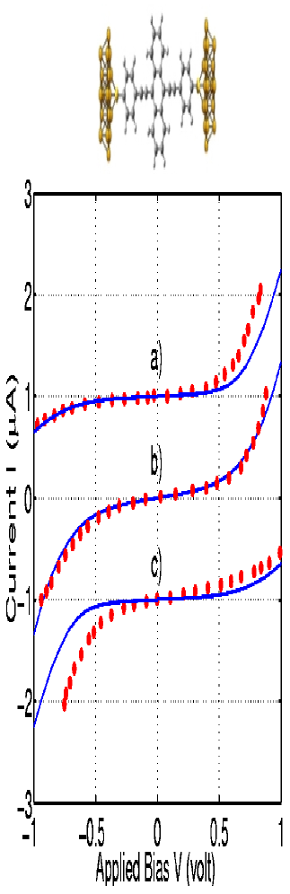
To illustrate charging induced I-V asymmetry we apply our self-consistent transport model to the symmetric molecule, [9,10-Bis((-para-mercaptophenyl)-ethinyl)-anthracene] (see top of Fig. 1) studied in a recent break junction measurement [13]. The curve (b) in Fig. 1 is obtained assuming ideal sulphur-gold bonding (2.53 ) on both sides of the molecule (symmetric coupling situation) on a gold-molecule-gold system. On the other hand, the curves (a) and (c) represent an asymmetric coupling situation where the asymmetry is introduced in the system by stretching the bond between sulphur and gold on the left side and the right side respectively by 0.65 . The sulphur-gold bond length has been treated as a fitting parameter which is justifiable as the exact bond length is not known from the experiment.
Another fitting parameter used in our calculation is a constant potential which is applied on the molecule (only on the whole molecule and not on any part of the gold contacts) in order to move the molecular energy levels up or down rigidly relative to the contact Fermi energy. The precise location of equilibrium Fermi energy can depend sensitively on many factors such as surface conditions, environmental situations, geometrical fluctuations etc. In the absence of detailed information of all these factors in a particular experimental set-up, it is necessary to treat the position of as an adjustable parameter. Thus we believe it is justifiable to include this adjustable parameter in our calculations to take into account of the effect of chrage transfer at equilibriumin and adjust the position of relative to the molecular energy levels. Our fitting requires that be closer to HOMO rather than LUMO i.e. the conduction is p-type. The Fermi energy of gold (within the EHT description) is kept fixed at -9.5 eV [20] and relative to this value the molecular energy levels are moved up by so that is set to be 0.33 eV.
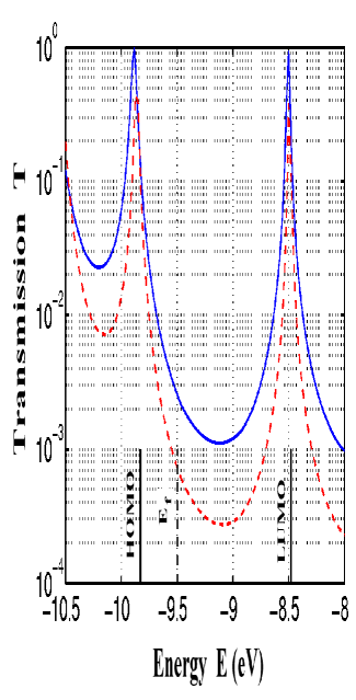
The calculated trend in the I-V characteristics agrees both in shape and current magnitude with the experimental result, as evident from Fig. 1. The agreement of our calculated current value with experiment suggests that the observed I-V is obtained for a near ideal gold-molecule-gold contact and the current is going through a single or at most a few number of molecules. In spite of stretching the S-Au bond by 0.65 the amplitude of current does not change appreciably. This can be explained by noting that the transmission coefficients do not differ significantly in the energy range of interest from -10 eV to -9 eV (see Fig. 2). The little discrepancy in the shape of the I-V can be attributed to the variation in the experimental results. It should also be noted that the same value for the constant potential (i.e. same ) is used to generate all the three curves in Fig. 1, though the position of the Fermi energy can conceivably be different for curves (a) and (c) as the experimental conditions are different. Indeed, by using slightly different values for within a justifiable range ( = 1.55 eV and = 1.6 eV for curves (a) and (c) respectively) we do obtain a better fit of the I-V (not shown).
In our calculations we assumed that the system is in the self-consistent field regime. This assumption should be valid as long as the energy level broadening due to contact coupling is comparable to (or greater than) the single-electron charging energy. We estimate these factors to be of the order of 0.2 eV and 1.5 eV, respectively. It should be further noted that the experimental current value is higher (of the order of A) than other typical experimental values, suggesting strong chemisorbed bonding between sulphur and gold at both ends. Thus we believe our assumption of self-consistent field approach is a correct one.
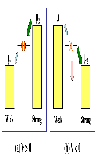
In order to explain the origin of this asymmetry in the I-V we need to understand the effect of asymmetric charging on molecular conduction. This is explained schematically in Fig. 3 for a simple single level model. Let us suppose that the contacts are strongly asymmetric (). For positive bias on the weak contact (Fig. 3a), the latter is trying to empty the nearest (HOMO) level, while the strong contact is trying to fill it, with the net result that the HOMO level stays filled. Current onset occurs at the voltage where first crosses the (neutral) molecular level. For opposite bias direction (Fig. 3b), however, the HOMO level is emptied out, which charges up the molecule positively. This adds a self-consistent charging energy that lowers the energy level, postponing thereby the point where the HOMO is crossed by . In effect, this stretches out the voltage axis in the I-V, leading thus to a smaller conductance for negative bias on the weak contact. For LUMO-based conduction the argument is reversed, since filling the LUMO level charges up the molecule negatively.
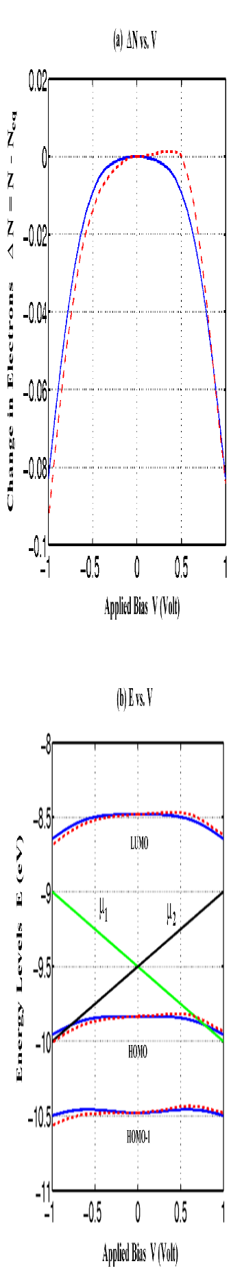
It can be seen from Fig. 4 that the number of electrons and the energy levels of the molecule change symmetrically with the applied bias for the symmetric coupling situation. This is expected for a symmetric system. However, in the asymmetric coupling situation the weakly coupled left contact can not fill up the HOMO level quickly enough and so this level remains more empty in the negative bias direction compared to that in the positive bias (Fig. 4a). This in turn makes the charging asymmetric and forces the energy levels to move down more in the negative bias direction (Fig. 4b).
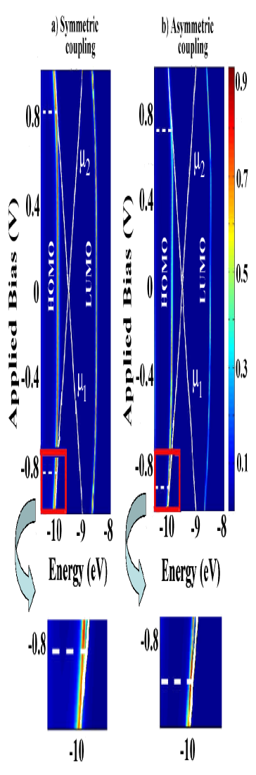
Fig. 5 shows a color plot of the transmission T(E,V), for symmetric coupling (a) and asymmetric coupling (b), corresponding respectively to curves (b) and (a) in Fig. 1. In both cases, the same HOMO level is crossed by the contact electrochemical potentials (white solid lines) leading to current conduction. For symmetrically coupled contacts, current starts flowing around V in both bias directions, leading to the symmetric I-V in Fig. 1b. For the asymmetrically coupled case, however, differential charging leads to a postponed onset of conduction at around -0.9 V for negative bias on the weak (left) contact, and an earlier onset at around +0.7 V for opposite bias polarity. This makes the current lower and stretched out in the negative bias direction which leads to the asymmetric I-V in Fig. 1a. The delay in the onset is seen clearer in the enlarged portions shown at the bottom of Fig. 5.
The charging induced asymmetry in the I-V also sheds light on whether the current conduction is p-type or n-type. If we would assume LUMO conduction in our calculations, the direction of asymmetry in the I-V would get reversed. Thus, from the knowledge of the coupling asymmetry and the I-V asymmetry we can predict whether it is HOMO or LUMO conduction. Although we do not know which contact is weaker for the break junction measurements, for similar measurements with STM [15] where the weaker contact is easily identified, this physics helps infer that conduction is p-type. Most often it is very difficult to pinpoint the position of Fermi energy relative to the molecular energy levels and so this ability of predicting conduction type is very desirable and useful. It should be noted that the nature of conduction could possibly be identified by other techniques, e.g. by using thermoelectric [28] or gating effects [29].
It is worthwhile pointing out that the I-V asymmetry discussed in this paper can not be explained solely in terms of asymmetry in the Laplace potential, neglecting charging effects altogether. Asymmetric charging gives conductance peaks of different heights at same voltage values (see Fig. 10 in [15]), in contrast to Laplace potential asymmetries which give conductance peaks at different voltages but of the same height.
In summary, we have achieved a quantitative agreement with experimentally observed asymmetric I-Vs and established that even for spatially symmetric molecules, contact asymmetry can induce an asymmetric I-V through asymmetric charging. The sense of the asymmetry depends on whether conduction is through a HOMO or a LUMO level.
We would like to thank P. Damle, R. Reifenberger, D. Janes and H. B. Weber for useful discussions. This work has been supported by NSF Network for Computational Nanotechnology and the US Army Research Office (ARO) under grants number EEC-0228390 and DAAD19-99-1-0198.
REFERENCES
- [1] C. Dekker, Phys. Today 52, 22 (1999).
- [2] H. Ohnishi, Y. Kondo and K. Takayanagi, Nature (London) 395, 780 (1998).
- [3] H. W. Fink and C. Schonenberger, Nature (London) 398, 407 (1999); D. Porath, A. Bezryadin, S. de Vries and C. Dekker, Nature (London) 403, 635 (2000).
- [4] M. A. Reed, C. Zhou, C. J. Muller, T. P. Burgin and J. M. Tour, Science 278, 252 (1997).
- [5] G. E. Poirier and M. J. Tarlov, Langmuir 10, 2853 (1994); G. Leatherman, E. N. Durantini, D. Gust, T. A. Moore, A. L. Moore, S. Stone, Z. Zhou, P. Rez, Y. Z. Liu and S. M. Lindsay, J. Phys. Chem. B 103, 4006 (1999).
- [6] B. Chen and J. M. Metzger, J. Phys. Chem. B 103, 4447 (1999).
- [7] J. Chen, M. A. Reed, A. M. Rawlett and J. M. Tour, Science 286, 1550 (1999).
- [8] N. P. Guisinger, M. E. Greene, R. Basu, A. S. Baluch, M. C. Hersam, Nano Lett. 52, 55 (2004).
- [9] A. Aviram and M. A. Ratner, Chem. Phys. Lett. 29, 274 (1974).
- [10] P. Damle, T. Rakshit, M. Paulsson and S. Datta, IEEE Transactions on Nanotechnology, 1, 145 (2002).
- [11] G-C. Liang, A. W. Ghosh, M. Paulsson and S. Datta, Phys. Rev. B 69, 115302 (2004).
- [12] C. Krzeminski, C. Delerue, G. Allan, D. Vuillaume and R. M. Metzger, Phys. Rev. B 64, 085405 (2001).
- [13] J. Reichert, R. Ochs, D. Beckmann, H. B. Weber, M. Mayor and H. v. Löhneysen, Phys. Rev. Lett. 88, 176804 (2002).
- [14] C. Kergueris, J. -P. Bourgois, S. Palacin, D. Esteve, C. Urbina, M. Magoga and C. Joachim, Phys. Rev. B 59, 12505 (1999).
- [15] W. Tian, S. Datta, S. Hong, R. Reifenberger, J. I. Henderson and C. P. Kubiak, J. Chem. Phys. 109, 2874 (1998).
- [16] M. Di Ventra, S. T. Pantelides and N. D. Lang, Phys. Rev. Lett. 84, 979 (2000).
- [17] P. S. Damle, A. W. Ghosh and S. Datta, Phys. Rev. B 64, 201403(R) (2001).
- [18] K. Stokbro, J. Taylor, M. Brandbyge, J.-L. Mozos and P. Ordejon, Comput. Mater. Sci. 27, 151 (2003).
- [19] E. G. Emberly and G. Kirczenow, Phys. Rev. B 58, 10911 (1998).
- [20] F. Zahid, M. Paulsson and S. Datta, “Electrical Conduction through Molecules”, Advanced Semiconductor and Organic Nano-techniques (III), H. Morkoc (Ed.), Academic Press (2003).
- [21] L. E. Hall, J. R. Reimers, N. S. Hush and K. Silverbrook, J. Chem. Phys. 112, 1510 (2000).
- [22] A. W. Ghosh and S. Datta, J. Comp. Elec. 1, 515 (2002).
- [23] S. Datta, “Electronic Transport in Mesoscopic Systems”, Cambridge University Press (1995).
- [24] S. Datta, W. Tian, S. Hong, R. Reifenberger, J. I. Henderson and C. P. Kubiak, Phys. Rev. Lett. 79, 2530 (1997).
- [25] J. A. Pople and G. A. Segal, J. Chem. Phys. 44, 3289 (1966).
- [26] J. N. Murell and A. J. Harget, “Semi-empirical SCF Theory of Molecules”, John Wiley & Sons (1972).
- [27] E. Polizzi and N. Ben Abdallah, Phys. Rev. B 66, 245301 (2002).
- [28] M. Paulsson and S. Datta, Phys. Rev. B 67, 241403 (R) (2003).
- [29] Jeong-O Lee, G. Lientschnig, F. Weirtz, M. Stuijk, R. A. J. Janssen, R. Egberink, D. N. Reinhoudt, P. Hadley and C. Dekker Nano Lett. 3, 113 (2003).