Surface-acoustic-wave driven planar light-emitting device
Abstract
Electroluminescence emission controlled by means of surface acoustic waves (SAWs) in planar light-emitting diodes (pLEDs) is demonstrated. Interdigital transducers for SAW generation were integrated onto pLEDs fabricated following the scheme which we have recently developed Cecchini et al. (2003). Current-voltage, light-voltage and photoluminescence characteristics are presented at cryogenic temperatures. We argue that this scheme represents a valuable building block for advanced optoelectronic architectures.
pacs:
72.50.+b,78.60.Fi,85.60.Jb,43.38.RhSurface acoustic waves (SAWs) are attracting much interest in semiconductor-device research owing to their interaction properties with quasi two-dimensional systems (2DSs). Lattice deformations induced by SAWs propagating on a piezoelectric substrate (i. e. GaAs) are accompanied by potential waves which interact with charge carriers confined in the heterostructure leading to energy and momentum transfer. This interaction can drag carriers along the SAW-propagation direction resulting in a net DC current or voltage, the acoustoelectric effect Esslinger et al. (1994, 1992); Campbell et al. (1992). Moreover, this same interaction induces changes in SAW velocity and amplitude that can be used to probe 2DSs transport properties Wixforth et al. (1986); Willett et al. (1993); Paalanen et al. (1992); Simon (1996).
Several devices were proposed and realized exploiting the acoustoelectric effect. Talyanskii et al. proposed the implementation of a novel current standard based on SAW-driven transport through a quantum point contact Cunningham et al. (2000, 1999); Ebbecke et al. (2000); Talyanskii et al. (1997); Shilton et al. (1996), demonstrating very precise quantization of the acousto-electric current down to single-electron transfer per wave cycle. A particularly appealing device proposal suggests the incorporation of a single-electron SAW pump in a planar 2D electron/2D hole gas (n-p) junction to realize a single-photon sourceFoden et al. (2000).
In this Letter we demonstrate one of the main building blocks of this latter single-photon source: we shall show transport and optical emission in planar light-emitting n-p devices (pLEDs)Cecchini et al. (2003) controlled by means of SAWs. With the pLED biased below threshold, the electric field associated with SAW propagation in the GaAs facilitates the extraction and transportation of electrons from the n-type region of the structure into the 2D hole gas (2DHG) region, thereby generating electroluminescence emission.
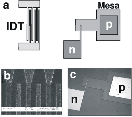
Devices were fabricated starting with a p-type modulation-doped Al0.3Ga0.7As/GaAs heterostructure grown by molecular beam epitaxy, containing a 2DHG within a 20-nm-wide GaAs quantum well embedded 70 nm below the surface. The measured hole density and mobility after illumination at 1.5 K were cm-2 and 35000 cm2/Vs, respectively. The heterostructure was processed into mesas with an annealed p-type Au/Zn/Au (5/50/150 nm) Ohmic contact. The fabrication of the n-type region of the junction started with the removal of the Be-doped layer from part of the mesa by means of wet etching (48 s in H3PO4:H2O2:H2O = 3:1:50) and evaporation of a self-aligned Ni/AuGe/Ni/Au (5/107/10/100 nm) n-type contact. After annealing, donors introduced by the n-type contact provide conduction electrons within the well. The n-contact was shaped as a thin stripe placed perpendicular to the SAW-propagation direction, 250 m away from the p-contact (see Figs. 1a and 1c). SAWs propagating along the (01̄1̄) crystal direction were generated by means of an interdigital transducer (IDT) composed of 100 pairs of 200 m-long Al fingers with 3 m periodicity (1 GHz resonance frequency on GaAs). Transducers were fabricated at a distance of 800 m from the mesa by electron-beam lithography (see Fig. 1b). The width of the n-type contact stripe (2 m) was chosen to be of the same order of magnitude as the SAW wavelength (3 m) in order to limit damping of the SAW electric field. A schematic view of the device is shown in Fig. 1.
Several pLEDs were fabricated with this protocol and preliminarily electrically tested; all exhibited similar characteristics. Fig. 2(a) shows the current-voltage (I-V) curves at different temperatures of one representative device, on which all the measurements reported in this Letter were taken. Rectifying behavior is observed with a threshold voltage V, consistent with the value expected for a GaAs p-n junction.
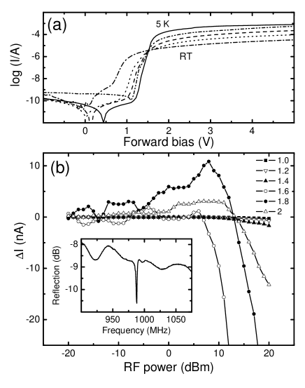
The SAW resonance frequency was determined by measuring the power reflected by the transducer as a function of excitation frequency. The transducer frequency response (see inset of Fig. 2(b)) displayed a dip at 987.5 MHz with a full width half maximum (FWHM) of 2.4 MHz, at 5 K, which is consistent with the periodicity of the transducer.
The effect of SAWs on the device transport properties was studied by measuring the change of the current () flowing out of the n-type contact (with the p-type contact grounded) with and without the presence of a SAW as a function of the power of the RF signal applied () to the IDT at several forward biases around device threshold (see Fig. 2(b)). The RF signal applied to the transducer was set at the measured resonance frequency of 987.5 MHz. was observed to increase (i.e. more electrons injected into the 2DHG) for biases in the range of 1.6 V to 2.0 V. This regime was observed for values of up to dBm. At very high power levels ( dBm) a reduction in is observed probably due to heat losses in the transducer and in the RF cable. These measurements demonstrate that the acoustoelectric effect can enhance the differential conductance of pLEDs near threshold.
SAW control of the junction optical emission was demonstrated by light-bias (L-V) measurements at low temperature (5 K) (see Fig. 3). Spectra as a function of bias were collected by a cooled CCD after spectral filtering by a single-grating monochromator. The electroluminescence (EL) spectra reported in the inset of Fig. 3(b) show a main peak at 818.7 nm (FWHM 1.8 nm) originating from radiative recombination within the QW and a secondary peak at 831.2 nm (FWHM 3.6 nm) which is known to originate from carbon impurities included in the heterostructure material during growth 111B. Hamilton, in Properties of Gallium Arsenide, edited by M. R. Brozel and G. E. Stillman (INSPEC, London, England, 1996).. Furthermore, the SAW can be seen to not change significantly the shape of the spectra.
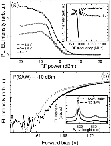
Figure 3(a) shows the effect of SAWs on the optical properties of the pLEDs. Light intensity, calculated by integration over the main EL peak from 810 nm to 826 nm, is reported as a function of (at transducer resonance frequency, 987.5 MHz) for two different values of forward bias. Two different regimes can be observed: an increase in EL intensity up to dBm followed by an abrupt suppression of the emission. The latter regime can be linked to the spatial separation between electrons and holes induced by the SAW electric field Rocke et al. (1997); Alsina et al. (2001), which is also observed in the PL measurements 222PL spectra were obtained by excitation of a region of the mesa with a red-light laser source (653 nm). (filled triangles in Fig 3(a)). Remarkably, the increase in intensity observed for dBm is unique to the EL measurements as it was not observed in the PL data. The resonant nature of this effect is shown in the inset of Fig. 3(a) where the light intensity is plotted as a function of the frequency of the signal applied to the IDT (RF-frequency) for dBm. A clear dip in both EL and PL data is present at the observed transducer resonant frequency. These observations and the measured increase of forward current in presence of SAWs demonstrate SAW-driven injection of electrons into the 2DHG leading to increased EL intensity.
This is further highlighted by the comparison between L-V data collected with and without SAWs shown in Fig 3(b), where the EL threshold is reduced from 1.65 V to 1.64 V in the presence of SAWs.
In conclusion we demonstrated the possibility of controlling the electroluminescence emission from a planar diode by means of surface acoustic waves. Planar-junction devices with interdigital transducers were fabricated and characterized by transport and optical measurements at cryogenic temperatures. We have demonstrated that SAWs can induce transport and light emission in these devices. SAW-driven light-emitting diodes are one of the fundamental building blocks of the single-photon source proposed in Ref. Foden et al. (2000). This work was supported in part by the European Commission through the FET Project SAWPHOTON and by MIUR within FISR “Nanodispositivi ottici a pochi fotoni”. We thank M. Lazzarino for technical help in device fabrication.
References
- Cecchini et al. (2003) M. Cecchini, V. Piazza, F. Beltram, M. Lazzarino, M. B. Ward, A. J. Shields, H. E. Beere, and D. A. Ritchie, Appl. Phys. Lett. 82, 636 (2003).
- Esslinger et al. (1994) A. Esslinger, R. W. Winkler, C. Rocke, A. Wixforth, J. P. Kotthaus, H. Nickel, W. Schlapp, and R. L sch, Surf. Sci. 305, 83 (1994).
- Esslinger et al. (1992) A. Esslinger, A. Wixforth, R. W. Winkler, J. P. Kotthaus, H. Nickel, W. Schlapp, and R. L sch, Solid State Commun. 84, 84 (1992).
- Campbell et al. (1992) J. W. M. Campbell, F. Guillon, M. D’Iorio, M. Buchanan, and R. J. Stoner, Solid State Commun. 84, 735 (1992).
- Wixforth et al. (1986) A. Wixforth, J. P. Kotthaus, and G. Weimann, Phys. Rev. Lett. 56, 2104 (1986).
- Willett et al. (1993) R. L. Willett, R. R. Ruel, K. W. West, and L. N. Pfeiffer, Phys. Rev. Lett. 71, 3846 (1993).
- Paalanen et al. (1992) M. A. Paalanen, R. L. Willett, P. B. Littlewood, R. R. Ruel, K. W. West, L. N. Pfeiffer, and D. J. Bishop, Phys. Rev. B 45, 11342 (1992).
- Simon (1996) S. H. Simon, Phys. Rev. B 54, 13878 (1996).
- Cunningham et al. (2000) J. Cunningham, V. I. Talyanskii, J. M. Shilton, M. Pepper, A. Kristensen, and P. E. Lindelof, Phys. Rev. B 62, 1564 (2000).
- Cunningham et al. (1999) J. Cunningham, V. I. Talyanskii, J. M. Shilton, M. Pepper, M. Y. Simmons, and D. A. Ritchie, Phys. Rev. B 60, 4850 (1999).
- Ebbecke et al. (2000) J. Ebbecke, G. Bastian, M. Blöcker, K. Pierz, and F. J. Ahlers, Appl. Phys. Lett. 77, 2601 (2000).
- Talyanskii et al. (1997) V. I. Talyanskii, J. M. Shilton, M. Pepper, C. G. Smith, C. J. B. Ford, E. H. Linfield, D. A. Ritchie, and G. A. C. Jones, Phys. Rev. B 56, 15180 (1997).
- Shilton et al. (1996) J. M. Shilton, V. I. Talyanskii, M. Pepper, D. A. Ritchie, J. E. F. Frost, C. J. B. Ford, C. G. Smith, and G. A. C. Jones, J. Phys.: Condens. Matter 8, L531 (1996).
- Foden et al. (2000) C. L. Foden, V. I. Talyanskii, G. J. Milburn, M. L. Leadbeater, and M. Pepper, Phys. Rev. A 62 (2000).
- Rocke et al. (1997) C. Rocke, S. Zimmermann, A. Wixforth, J. P. Kotthaus, G. Böhm, and G. Weimann, Phys. Rev. Lett. 78, 4099 (1997).
- Alsina et al. (2001) F. Alsina, P. V. Santos, R. Hey, A. Garc a-Crist bal, and A. Cantarero, Phys. Rev. B 64 (2001).